

New P2 module
 knivd
Posts: 104
knivd
Posts: 104
Hi All,
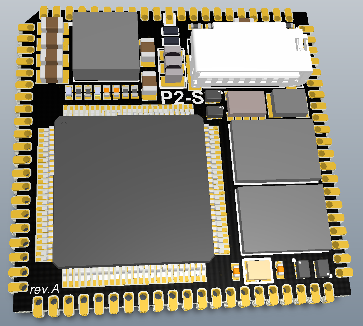
Here is something new, on which I have been working for a while. A chip-scale P2-STAMP module, which is only about 30x30mm in size, and fits into a standard PLCC-84 socket. My history with making this type of chipscale modules goes back to the late 2000's. The previous last I made was the Configum-2 FPGA module a few years ago. I discovered the P2 relatively short while ago, and immediately loved its concept since it closely represents what I see a modern MCU should be like. I also think the P2-STAMP would provide a great embeddable module for real-world applications with the P2.
The parameters of the P2-STAMP:
- Built-in high-current power supply with protection and external rails
- Propeller 2 with 20 MHz crystal
- 16MB flash memory
- 16MB HyperRAM
- Real-Time clock with backup supercapacitor
- Micro SD slot (facing inwards for increased reliability)
- Two on-board LEDs
- Configuration and glue logic
- All supporting passive components
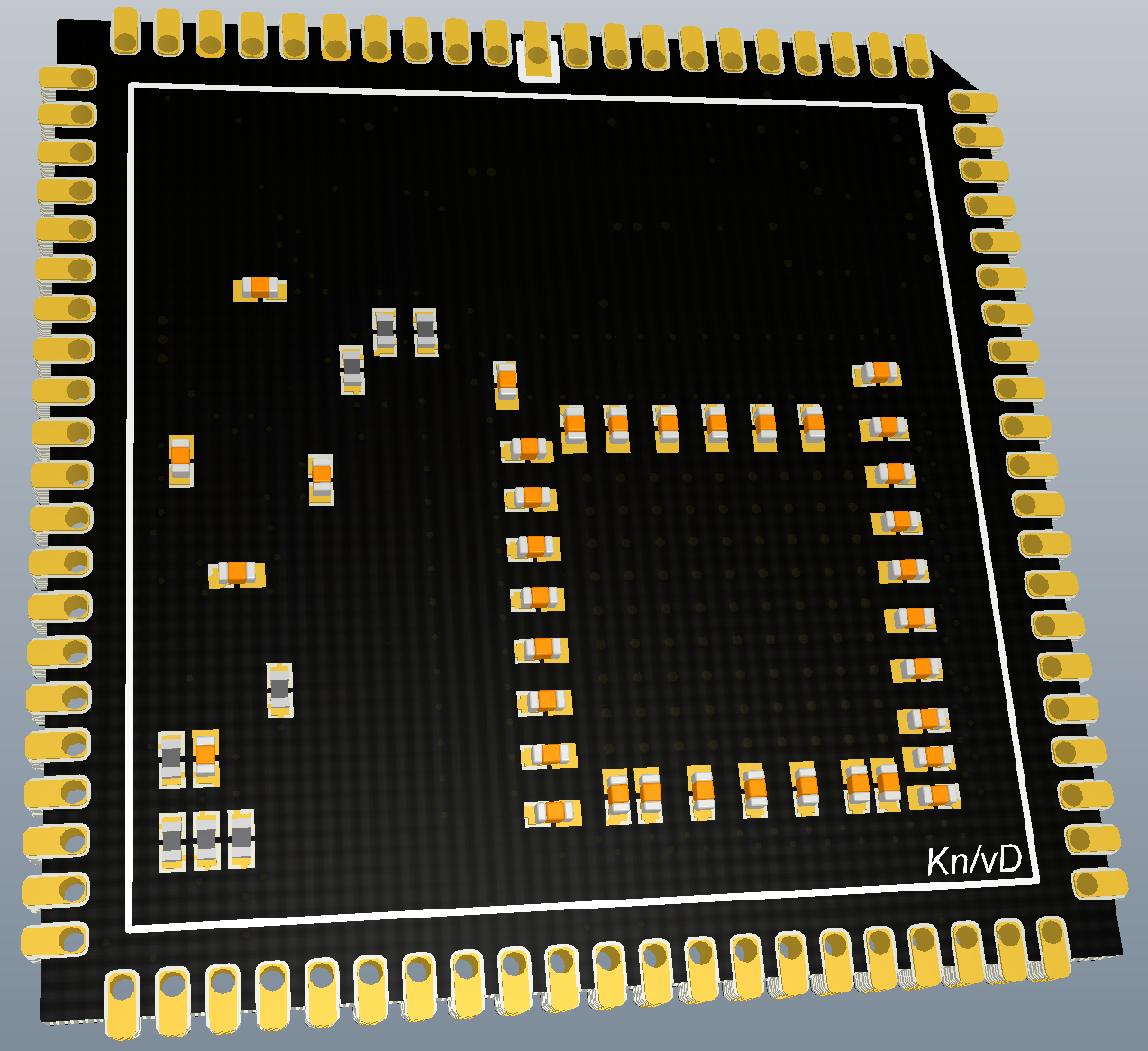
The size of the flash and RAM are purely chosen on the basis of current Digikey stock availabilities, and can be downgraded or upgraded as per specific needs. The HyperRAM uses an 8-bit bus, thus releasing more of the Propeller's smart I/O's to the outside world. All the Propeller's I/O are accessible from outside with 47 out of the 64 I/O lines completely free from any load. All I/O's are also reasonably length-matched within the module for ensuring correct operation of high-speed interfaces. There are several configuration pins that determine the module's behaviour and what is enabled on it.
This is the earliest announcement in the public space about the P2-STAMP.
I am currently producing early samples and an explorer breakout board for prototyping with it, soon to appear on the Crowd Supply platform.
Would there be any interest in the P2-STAMP in this group?
Comments
That's very compact!
What interests me the most is tight coupling of HyperRAM for possible performance. There is real possibility for significant bandwidth, 1:1 with max streamer rate, if the signal characteristics of clocking suits it. Have you followed any of the testing we've done using the Eval boards with HyperRAM add-on board?
One problem we struck was the parallel busing to both HyperRAM and HyperFlash made the data lines slower than the clock lines (The clocks to the two memories are independent on the add-on board). The timings needed to be the other way around to make write-data setup requirement at 1:1 (sysclock/1 transfer rate).
Very neat. Like it!
How many layers are you going for ? Have you figured out the stack-up yet to be able to route all that ?
I like the clean alignment on the front, although the crystal might be better moved closer to the P2 package in that gap you have.
Heat dissipation might be an issue with those rear-side parts. Might need some thought at higher speeds/loads.
I'd be interested in trying it out for sure! Keep us posted!
Very neat! Can you give us a ballpark idea about small quantity (1-10) pricing?
Nice. For future video projects I might like to do, this could be a handy board. I like the idea it could fit a PLCC socket which allows for some simple prototyping early on and then remains re-usable later.
Regarding the hyperRAM routing, I don't have the Parallax's board, so can't test its performance, but technically in the design I have observed everything that needs observing. Of course, this is preliminary information and the real performance will become known only after having the prototypes tested. There might be some further revisions needed later, too. Also, the flash is not on the same bus as the RAM.
On the question about the PCB, yes it is done and currently in the factory. There is a bit of delay because of the Chinese New Year holidays, but I hope to hold the prototypes in my hand sometime later in February.
It is a 8-layer PCB, and in terms of cost, the BOM is close to the current Edge module. Subject to further optimisations, of course.
I've put the crystal as close to the P2's inputs as physically possible. The two surrounding caps are normally DNF, although they appear in the render. On the bottom there are only 0402 size passives, and there is a perforated polygon under the P2. Three out of the eight layers are full coper ground for maximum heat dissipation. I have taken as much care as I could to avoid the need of having a heatsink glued on top of it, but it may still be needed, we will see later
Please! Do keep us posted with your project!
A very neat small board") With RAM! What about voltages - are there regulators onboard or 3v3 and 1v8 have to be externally supplied?
With RAM! What about voltages - are there regulators onboard or 3v3 and 1v8 have to be externally supplied?
So, it's a yes to me. That brick at the top left looks the part (at the very first picture).
Very interesting!
At first glance, it looks like a direct competitor to the P2 Edge modules.
The standard socket and lying flat profile are probably advantages for professional use.
I've never used that type of socket, but looks fine.
How are you handling boot selection?
The Edge uses dip switches.
Personally, I'd just have it set to always boot from flash (after trying serial).
I need to make clear that the goal of P2-STAMP is not to compete with the Edge module. Each has their own niche of possible applications. In the ideal case I am more than happy to cooperate with Parallax in case the team is interested.
More choice for the user only benefits the wider adoption of the P2 processor.
The original drive for me designing this module was a project which I had initially started around the Edge module, but then hit some practical challenges with its format and the slot itself. The Stamp is supposed to be installed into a socket, but also with a 25x25mm cutout on the PCB underneath can be installed directly on to an end product PCB. And also on four 1.27mm headers.
Regarding the dip switches, there are none, but there are several allocated pins on the module which perform the same functions and a few more in regard to configuring what is enabled and the power supply mode.
And yes, there are both 3.3V and 1.8V supplies, 2.5A on each rail, and they are also available to feed outside circuits as much as the power budget allows.
Input is in the range 3.6V - 20V.
I mentioned what we had tested already as a reference to the difficulties only.
Separate data pins sounds good. The one recommendation I would've made is to ensure the clock pin had the longest route.
The plan in my head is to make use of registered I/O pin mode to give the data pins a slight timing advance over the clock pin. We tested this already with the Eval Board setup but it wasn't enough to overcome the layout biases.
That's a valuable recommendation. Just had a look at the layout, and unfortunately the clock is not the longest trace there, but I can make it so. Will check with the factory, and with some luck if they have not yet put the PCB into production, may even try it out on the first run...
The delay from pin to core varies by up to 850ps among pins, I believe.
Cool. Actually there is one other idea, that I didn't fully understand the numbers for - There was a spreadsheet that had come from OnSemi's timing analysis of the Prop2's I/Os. It showed the relative input and output propagation delays of each I/O pin.
From that spreadsheet one could then pick an advantageous pin for something like a clock pin.
Ah, Chip. Is it okay for me to post that spreadsheet here?
That's nice, but is it really that much critical? The hyperRAM itself can only go up to 200MHz, so shaving a few ps off here or there would not change the outcome by much, I suppose?
Actually, the one I've got has this comment
It allows 1:1 sysclock ratio instead of limited to 1:2. Makes use of DDR feature.
EDIT: And the HR overclocks just fine, btw. We've well exceeded 200 MB/s, with broad data verification, in extensive testing on the Eval Boards + add-on. There was certain difficult frequency bands but the expectation is that'll improve with better layout. So I'm on the hunt for such.
I have routed it in a way to stay within the DDR3 recommended length matching, so that is for 800MHz rates which is way more than what this hyperRAM can do, so (keeping fingers crossed) I hope it will be all right even at double rate
Absolutely!!
The important times for the HR clock is the outgoing propagation. It's the data write setup time that needs a lagging clock to achieve 1:1. So the pin for it should have larger output delay figure than all the data pins.
For data read timing probably the most important requirement is matching the eight data pins to themselves. The less timing variation between the eight bits the better.
EDIT: Although, I don't think there is any data in there that covers registered I/O propagations. So somewhat unsure how useful that particular spreadsheet is here.
If I was to pick I'd use P40-P47 for data and P39 for clock. Or P57 for clock would be good option if that's more suitable.
EDIT2: There's two distinctly poor data pin-groups for read timing: P16-P23 (832 ps input spread) and P48-P55 (548 ps input spread). And third worst is 352 ps input spread on P8-P15.
Throwing my own hat into the ring here - I think that would be a fascinating little gizmo.
Had a similar project in mind with a similarly socketable FPGA from a Japanese outfit, but the project collapsed before going very far. Def. interested in trying that with a P2. S.
Nice board, indeed!
Adding to what Von Szarvas said at post #4, about moving the crystal to a place the closer possible to P2 XI/XO pins, it's also important to remember avoiding any stubs/vias at those two paths; thus, at the two DNF external capacitors "perhaps-unused" land patterns at those paths can represent an impedance discontinuity, causing unwanted reflections, and "reviving" some bad outcomes due any use of pins[28:31] (V2831 also brings 3.3V to the PLL biasing circuit) that can be cause of "feeding" noisy signals into the internal crystal oscillator, affecting the PLL stability.
Another interesting possibility would be having the choice of mounting two HyperRam devices, instead of one HyperRam, and one HyperFlash. The solelly difference would be at the position of chip Enable line, a low-frequency signal, so a solder-selectable jumper can be used to re-route that signal, based on a decision made at assembly time.
Please, keep us posted as you progress...
Henrique
The P2 Edge has a TCXO option, maybe there is room to fit a 2016 oscillator, thus dispensing with the optional caps and removing any crosstalk problems ?
This could be a cheap default ? https://www.lcsc.com/product-detail/Oscillators_Yangxing-Tech-OT201620MJBA4SL_C669079.html
and there are TCXO in 2016 packages, but not so easy to nail down right now. ( eg ECS-TXO-2016-33-200)
Well, things can never be ideal...") P48-P55 are used for the RAM data line, and moving them across to another group would be way too much pain while I am not fully convinced about the need. But I am sure that it should be fine now, maybe with the exception of some overclocking niche application, which is not the target anyway, and I have already increased the length of the clock line (P47) to surpass all the others.
P48-P55 are used for the RAM data line, and moving them across to another group would be way too much pain while I am not fully convinced about the need. But I am sure that it should be fine now, maybe with the exception of some overclocking niche application, which is not the target anyway, and I have already increased the length of the clock line (P47) to surpass all the others.
Two HyperRAMs will not be possible, because the flash although physically in the same package, is SPI. It will be possible however, to install a bigger hyperRAM in its own footprint, because they all share the same regardess the internal size.
The crystal is indeed 2016 with no vias or stubs in the clock path. I will check if it can be moved even closer, and whether it will be possible to provide for selectable oscillator/crystal configuration.
I was wondering how the Flash part fitted with 47 free pins.
Yes, it is a well-thought design decision. Given the rationale of this module, I have concluded that maximum uncommitted smart I/O is much more universal variant than specifically targeting raw memory performance.
I have now moved the crystal even closer to the P2, and there are installation options for either a crystal or an oscillator on board.
Sounding good.
If there is room for an optional series cap, you can support clipped-sine TCXO too ?
I notice Epson list TCXO CMOS Osc down to 2520, but clipped sine go down to 2016 & 1612,
Are TCXO not logic level outputs? I would've thought "CMOS" implied they are.