Price I don't know about yet. Hoping they can be similar at least.
But, PCB was $14 each for Qty.50 and P2 is $16.
The real issue is the DC-DC converter chip at $14 each. It's something special with integrated inductor, but you have to pay for that.
Also, it seems to be a rare thing and could go out of stock at any time...
A smaller difference perhaps is the 8-bit bus hyperram vs 16-bit bus PSRAM. HyperRam uses less pins, so that is good.
Also, can turn off hyperram if you don't need it and get those pins back.
Suppose the RTC module is a another, perhaps less important, but useful feature for things I'm doing.
Nice to have the actual time for datalogging...
@Rayman said:
Also, can turn off hyperram if you don't need it and get those pins back.
That frustrated me a little when I realised that was so. HyperRAM is most effective when paired with fastest sysclock/1 timings. Any degradation from track length will reduce effectiveness.
I guess I should invest some time experimenting how well the P2Stamp's arrangement works when those PLCC contacts aren't connected. I'll need to solder it into place ... which means I need to do a carrier board layout too ...
@Rayman said:
Also, can turn off hyperram if you don't need it and get those pins back.
That frustrated me a little when I realised that was so. HyperRAM is most effective when paired with fastest sysclock/1 timings. Any degradation from track length will reduce effectiveness.
Is there any board that really manages sysclk/1 (at useful sysclk)?
Also when looking through those datasheets, I realized that with the output clocks we're running at sysclk/2, we should really set the latency count to 3. I think both my code and Roger's driver just rely on the default 6 or 7 setting, which is quite terrible.
(incidentally, with that allegedly upcoming 16x chip, if you could run it sysclk/1, you'd beat the EC32MB in bandwidth)
@Wuerfel_21 said:
Is there any board that really manages sysclk/1 (at useful sysclk)?
No, but there's only the one - An Eval add-on, implicit long tracks ... and data pins shared with HyperFlash chip makes the clock lead the data, which is in conflict with using a clock lagging capacitor or resistor.
@evanh I have both the Eval add-on and the P2STAMP, so that's two already. I usually use the former to test my HyperRAM codepaths - though I'm not sure how many people actually have the Hyper add-on board, like, is it worth the trouble?
@Wuerfel_21 said:
Also when looking through those datasheets, I realized that with the output clocks we're running at sysclk/2, we should really set the latency count to 3. I think both my code and Roger's driver just rely on the default 6 or 7 setting, which is quite terrible.
(incidentally, with that allegedly upcoming 16x chip, if you could run it sysclk/1, you'd beat the EC32MB in bandwidth)
I believe I had an API that can change the latency count for HyperRAM but it's not automatic configured based on P2 frequency so probably just defaults to the reset startup value by default. I've not looked at any HyperRAM for quite some time. I vaguely recall that the memory on the P2 Stamp I received had a slightly different timing to the original V1 HyperRAM the driver was based on and may have needed a tweak in the code to set it correctly.
Ye, the winbond part on the stamp defaults to 7 cycles, the eval addon defaults to 6 cycles. The exact given clock limit for 3 cycle seems to not be consistent between manufacturers, but 4 cycles is always safe for P2 sysclk/2 operation. For not-so-extreme overclocking, 3 cycles is the way. Should maybe figure this out next time I work with HyperRAM.
@Rayman said:
Edge and this are very similar.
Guess the real benefit is size.
Stamp is ~1.25"x1.25" for an area of 1.56 sq.in., if mounted using headers instead of PLCC-80 socket.
Edge (with uSD and PSRAM) is ~2.2" x 2.2" for an area of 4.8 sq.in.
So, that's a big difference, 3X smaller...
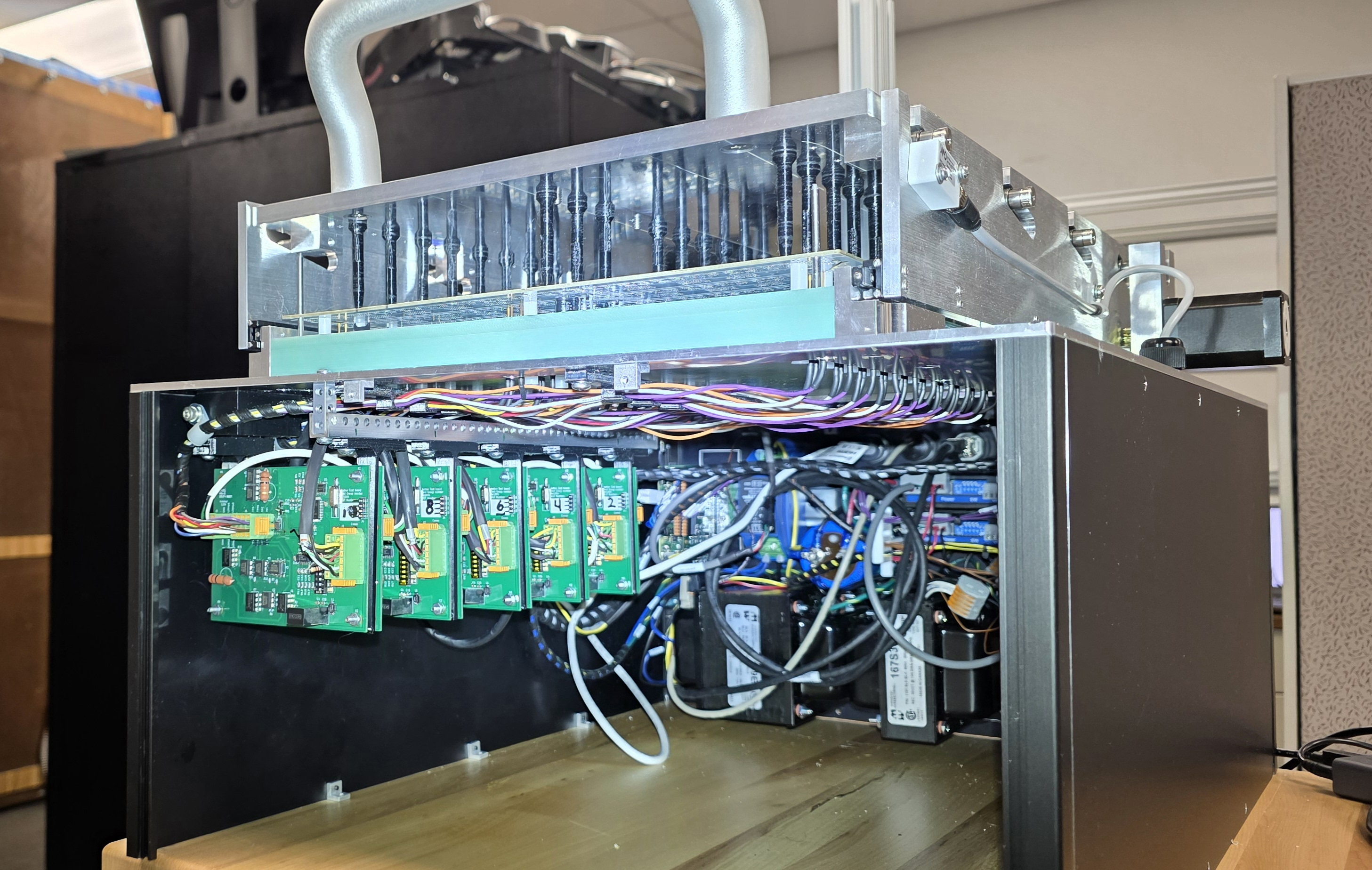
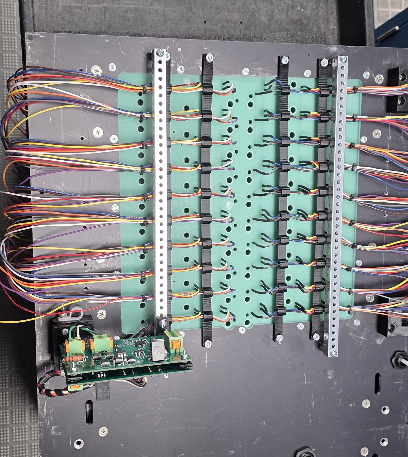
Yes, smaller and flatter if I cut out my board so this can solder down flush. My applications end up really dense, looking like this: (Yes, these just use P1)
Yes, this top photo is a tester for an entire panel of 10 units to be tested. The panel is 11-1/2"X11-1/2" The largest size our MFG plant wants to tackle.
The one being wired (bottom photo) is for a panel of 20 units in a similar size. The 'Spikes' apply pressure and when the lid is closed, those cams (Metal with angled slots) will motor forward, tightening the lid straight down with up to 30 KG of force to compress all the spring supports and 'pogos' that will make contact with the test points on the units.
Each unit gets it's own P1 board that does the entire inspection, then reports the results to the OBC that informs the operator that everything passed, or which units failed, and why. Those boards are custom for this line.
There are commercial units to do all of this, but MFG wants this linear close, and the number of test points demands some motorized help closing. We can build this for a fraction of the cost of the 'big boys'.
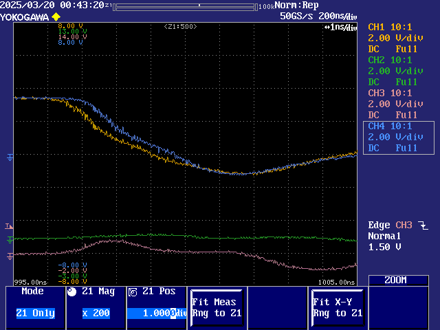
I've started testing the HyperRAM on this P2Stamp module. Looks like stability of the Prop2 itself hits a brick wall at around 360 MHz sysclock - Drawing 1.1 Watt from the 12 Volt supply so shouldn't be the onboard LTM4622 regulator limiting things. It's good for delivering 2.5 Amps x 1.8 Volts = 4.5 Watts. It's actually behaving like thermally crashing but there's no heat that I've noticed, so not too sure of why just yet.
I just measured the 1v8 rail and it is 1.81 Volts. Comparing to my testing Eval board which is 1.86 Volts and can achieve 370 MHz with light loads. That small difference in voltage right there may explain the difference in useable max frequency. I'd entirely overlooked this interaction in the past.
That's fine really. Its heat-sinking ability is limited, so when compute loaded it'll be better to operate at a lower voltage so as to reduce the amount of heat generation.
Well, the old version 2 tester from a couple years back is doing well. I haven't touched the low level parts and it's already producing great results on the P2Stamp module at sysclock/1. No capacitor added.
When using registered tx data + unregistered clock I get up to 310 MHz sysclock before data corruption sets in. But when using unregistered tx data + registered clock I get up to 330 MHz sysclock before data corruption sets in. Going by historical evidence, a registered clock has always produced greater range with reading performance. So I suspect the limit is still with the data reads than writes. Which will be nice to know. I'll have a look with the scope tonight. Also still to test all pin combinations for read data. I might still get lucky for 340 MHz say.
So I might have cracked the write timings already. It simply needs a clean direct signal path so that when the clock pin is using opposite registration to data pins, that provides enough phase shift all by itself.
PS: u/r columns below are for reading data pins unregistered and registered respectively. Applied at the command-data turnaround transition.
It's a pity that sysclk/1 starts to fail out around 334MHz and can't be coaxed to perform ~10MHz higher since this is right around the operating P2 clock range of the emulators Ada wrote. A sysclk/2 transfer byte rate is hopefully still good enough for running them though.
And here's same timings using an Eval board with the Hyper add-on plain, no added capacitor:
PS: I do get a lot of 100% results using base pin 0 but it's still scrappy with holes in the middle.
@rogloh said:
It's a pity that sysclk/1 starts to fail out around 334MHz and can't be coaxed to perform ~10MHz higher since this is right around the operating P2 clock range of the emulators Ada wrote. A sysclk/2 transfer byte rate is hopefully still good enough for running them though.
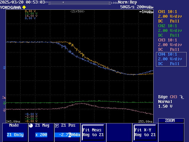
Yep, sysclock/2 is fine right up to crashing from hubRAM errors.
I've now completed all combinations at sysclock/1 - Which turned out to only be CLK registering, RXDAT registering and RXDAT Schmitting. Inverting CLK polarity has no effect on the RAM's responses since transactions are fixed to first rising clock edge after CE goes low. It ignores any half cycles.
Results were all worse than I already had. The posted sysclk/1 example above, that petered out at 330 MHz, is the best result - Registered CLK, Unregistered DAT.
It can still be improved using temperature and voltage management of course.
EDIT: Here's a small amount of cooling. It helps enough to get to 370 MHz sysclock without crashing. The 100% line makes it to 338 MHz. Some improvement. Stepping the voltage up to 1.9 Volts I expect will give a good improvement. I'll need to find a 27k ohm SMD resistor to do that.
Gearing up for P2 Stamp assembly using new PandaPlacer (OpenPNP based).
The Eagle export from the original Altium was very useful here as was able to export the part locations into the OpenPNP software using a ULP.
Just tested placing the P2 chip and it looks good.
The RTC that @knivd picked has some interesting features...
Integrated crystal is nice with such a small package. A lot smaller that the DS one. Says its under vacuum inside. That's interesting... Guess the crystal is moving around in there and doesn't want air stopping it...
Noticed it has a temperature sensor. That could be useful to answer questions about if the Stamp is getting hot when inside a case with little airflow.
The 8 bytes of user RAM is interesting too. For control applications, having something that retains state even after power failure is nice. Have to think about if this has any practical value, when one could just save things to flash or uSD...


Comments
Price I don't know about yet. Hoping they can be similar at least.
But, PCB was $14 each for Qty.50 and P2 is $16.
The real issue is the DC-DC converter chip at $14 each. It's something special with integrated inductor, but you have to pay for that.
Also, it seems to be a rare thing and could go out of stock at any time...
A smaller difference perhaps is the 8-bit bus hyperram vs 16-bit bus PSRAM. HyperRam uses less pins, so that is good.
Also, can turn off hyperram if you don't need it and get those pins back.
Suppose the RTC module is a another, perhaps less important, but useful feature for things I'm doing.
Nice to have the actual time for datalogging...
That frustrated me a little when I realised that was so. HyperRAM is most effective when paired with fastest sysclock/1 timings. Any degradation from track length will reduce effectiveness.
I guess I should invest some time experimenting how well the P2Stamp's arrangement works when those PLCC contacts aren't connected. I'll need to solder it into place ... which means I need to do a carrier board layout too ...
Is there any board that really manages sysclk/1 (at useful sysclk)?
Also when looking through those datasheets, I realized that with the output clocks we're running at sysclk/2, we should really set the latency count to 3. I think both my code and Roger's driver just rely on the default 6 or 7 setting, which is quite terrible.
(incidentally, with that allegedly upcoming 16x chip, if you could run it sysclk/1, you'd beat the EC32MB in bandwidth)
No, but there's only the one - An Eval add-on, implicit long tracks ... and data pins shared with HyperFlash chip makes the clock lead the data, which is in conflict with using a clock lagging capacitor or resistor.
@evanh I have both the Eval add-on and the P2STAMP, so that's two already. I usually use the former to test my HyperRAM codepaths - though I'm not sure how many people actually have the Hyper add-on board, like, is it worth the trouble?
I meant there was only one other before the P2Stamp. It was impossible to make reliable at sysclock/1. I lost interest after that.
@knivd
Very interested. I would enjoy purchasing one when you get it finished.
Martin
And since I am here "HELLO" to @evanh
I believe I had an API that can change the latency count for HyperRAM but it's not automatic configured based on P2 frequency so probably just defaults to the reset startup value by default. I've not looked at any HyperRAM for quite some time. I vaguely recall that the memory on the P2 Stamp I received had a slightly different timing to the original V1 HyperRAM the driver was based on and may have needed a tweak in the code to set it correctly.
Ye, the winbond part on the stamp defaults to 7 cycles, the eval addon defaults to 6 cycles. The exact given clock limit for 3 cycle seems to not be consistent between manufacturers, but 4 cycles is always safe for P2 sysclk/2 operation. For not-so-extreme overclocking, 3 cycles is the way. Should maybe figure this out next time I work with HyperRAM.
Yes, smaller and flatter if I cut out my board so this can solder down flush. My applications end up really dense, looking like this: (Yes, these just use P1)
or this. There will be 20 boards on it..
Okay, what is that? Is that a ginormous circuit board lying flat under the grid of spikes?
Yes, this top photo is a tester for an entire panel of 10 units to be tested. The panel is 11-1/2"X11-1/2" The largest size our MFG plant wants to tackle.
The one being wired (bottom photo) is for a panel of 20 units in a similar size. The 'Spikes' apply pressure and when the lid is closed, those cams (Metal with angled slots) will motor forward, tightening the lid straight down with up to 30 KG of force to compress all the spring supports and 'pogos' that will make contact with the test points on the units.
Each unit gets it's own P1 board that does the entire inspection, then reports the results to the OBC that informs the operator that everything passed, or which units failed, and why. Those boards are custom for this line.
There are commercial units to do all of this, but MFG wants this linear close, and the number of test points demands some motorized help closing. We can build this for a fraction of the cost of the 'big boys'.
I've started testing the HyperRAM on this P2Stamp module. Looks like stability of the Prop2 itself hits a brick wall at around 360 MHz sysclock - Drawing 1.1 Watt from the 12 Volt supply so shouldn't be the onboard LTM4622 regulator limiting things. It's good for delivering 2.5 Amps x 1.8 Volts = 4.5 Watts. It's actually behaving like thermally crashing but there's no heat that I've noticed, so not too sure of why just yet.
360MHz is pretty good though. Above where my 4-layers can reliably get to without raising the core voltage…
Probably a lot higher freq than anyone would use in the field…
Also above where @Wuerfel_21 emulators operate…
True, it is.
I just measured the 1v8 rail and it is 1.81 Volts. Comparing to my testing Eval board which is 1.86 Volts and can achieve 370 MHz with light loads. That small difference in voltage right there may explain the difference in useable max frequency. I'd entirely overlooked this interaction in the past.
That's fine really. Its heat-sinking ability is limited, so when compute loaded it'll be better to operate at a lower voltage so as to reduce the amount of heat generation.
I'm happy it's explainable.
Could increase value of the power supply feedback resistor and boost Vdd.
Don't think will for Stamp though...
Well, the old version 2 tester from a couple years back is doing well. I haven't touched the low level parts and it's already producing great results on the P2Stamp module at sysclock/1. No capacitor added.
When using registered tx data + unregistered clock I get up to 310 MHz sysclock before data corruption sets in. But when using unregistered tx data + registered clock I get up to 330 MHz sysclock before data corruption sets in. Going by historical evidence, a registered clock has always produced greater range with reading performance. So I suspect the limit is still with the data reads than writes. Which will be nice to know. I'll have a look with the scope tonight. Also still to test all pin combinations for read data. I might still get lucky for 340 MHz say.
So I might have cracked the write timings already. It simply needs a clean direct signal path so that when the clock pin is using opposite registration to data pins, that provides enough phase shift all by itself.
PS: u/r columns below are for reading data pins unregistered and registered respectively. Applied at the command-data turnaround transition.
DATA_PIN = 48 addpins 7 DQS_PIN = 56 addpins 0 CLK_PIN = 47 addpins 0 CE_PIN = 46 addpins 0 TX_REGD = 0 CLK_REGD = 1 CLK_ADV = -1 Data rate = (sysclock/1) Test data length: 100 x 1024 = 102400 bytes Frequency dependent lag compensation Sysclock u0 r0 u1 r1 u2 r2 u3 r3 u4 r4 u5 r5 60 MHz 0% 0% 0% 0% 100% 100% 0% 0% 0% 0% 0% 0% 62 MHz 0% 0% 0% 0% 100% 100% 0% 0% 0% 0% 0% 0% 64 MHz 0% 0% 0% 0% 100% 100% 0% 0% 0% 0% 0% 0% 66 MHz 0% 0% 0% 0% 100% 100% 0% 0% 0% 0% 0% 0% 68 MHz 0% 0% 0% 0% 100% 100% 0% 0% 0% 0% 0% 0% 70 MHz 0% 0% 0% 0% 100% 100% 0% 0% 0% 0% 0% 0% 72 MHz 0% 0% 0% 0% 100% 100% 0% 0% 0% 0% 0% 0% 74 MHz 0% 0% 0% 0% 100% 100% 0% 0% 0% 0% 0% 0% 76 MHz 0% 0% 0% 0% 100% 100% 0% 0% 0% 0% 0% 0% 78 MHz 0% 0% 0% 0% 100% 100% 0% 0% 0% 0% 0% 0% 80 MHz 0% 0% 0% 0% 100% 100% 0% 0% 0% 0% 0% 0% 82 MHz 0% 0% 0% 0% 100% 100% 0% 0% 0% 0% 0% 0% 84 MHz 0% 0% 0% 0% 100% 100% 0% 0% 0% 0% 0% 0% 86 MHz 0% 0% 0% 0% 100% 100% 0% 0% 0% 0% 0% 0% 88 MHz 0% 0% 0% 0% 100% 100% 0% 0% 0% 0% 0% 0% 90 MHz 0% 0% 0% 0% 100% 100% 0% 0% 0% 0% 0% 0% 92 MHz 0% 0% 0% 0% 100% 100% 0% 0% 0% 0% 0% 0% 94 MHz 0% 0% 0% 0% 100% 100% 0% 0% 0% 0% 0% 0% 96 MHz 0% 0% 0% 0% 100% 100% 0% 0% 0% 0% 0% 0% 98 MHz 0% 0% 0% 0% 100% 100% 0% 0% 0% 0% 0% 0% 100 MHz 0% 0% 0% 0% 100% 100% 0% 0% 0% 0% 0% 0% 102 MHz 0% 0% 0% 0% 100% 100% 0% 0% 0% 0% 0% 0% 104 MHz 0% 0% 0% 0% 100% 100% 0% 0% 0% 0% 0% 0% 106 MHz 0% 0% 0% 0% 100% 100% 0% 0% 0% 0% 0% 0% 108 MHz 0% 0% 0% 0% 100% 100% 0% 0% 0% 0% 0% 0% 110 MHz 0% 0% 0% 0% 100% 100% 0% 0% 0% 0% 0% 0% 112 MHz 0% 0% 0% 0% 100% 100% 0% 0% 0% 0% 0% 0% 114 MHz 0% 0% 0% 0% 100% 100% 0% 0% 0% 0% 0% 0% 116 MHz 0% 0% 0% 0% 93% 100% 0% 0% 0% 0% 0% 0% 118 MHz 0% 0% 0% 0% 15% 100% 0% 0% 0% 0% 0% 0% 120 MHz 0% 0% 0% 0% 0% 100% 0% 0% 0% 0% 0% 0% 122 MHz 0% 0% 0% 0% 0% 100% 0% 0% 0% 0% 0% 0% 124 MHz 0% 0% 0% 0% 0% 100% 0% 0% 0% 0% 0% 0% 126 MHz 0% 0% 0% 0% 0% 100% 77% 0% 0% 0% 0% 0% 128 MHz 0% 0% 0% 0% 0% 100% 100% 0% 0% 0% 0% 0% 130 MHz 0% 0% 0% 0% 0% 100% 100% 0% 0% 0% 0% 0% 132 MHz 0% 0% 0% 0% 0% 100% 100% 0% 0% 0% 0% 0% 134 MHz 0% 0% 0% 0% 0% 100% 100% 0% 0% 0% 0% 0% 136 MHz 0% 0% 0% 0% 0% 100% 100% 0% 0% 0% 0% 0% 138 MHz 0% 0% 0% 0% 0% 100% 100% 0% 0% 0% 0% 0% 140 MHz 0% 0% 0% 0% 0% 100% 100% 0% 0% 0% 0% 0% 142 MHz 0% 0% 0% 0% 0% 100% 100% 0% 0% 0% 0% 0% 144 MHz 0% 0% 0% 0% 0% 100% 100% 0% 0% 0% 0% 0% 146 MHz 0% 0% 0% 0% 0% 100% 100% 0% 0% 0% 0% 0% 148 MHz 0% 0% 0% 0% 0% 100% 100% 0% 0% 0% 0% 0% 150 MHz 0% 0% 0% 0% 0% 100% 100% 0% 0% 0% 0% 0% 152 MHz 0% 0% 0% 0% 0% 100% 100% 0% 0% 0% 0% 0% 154 MHz 0% 0% 0% 0% 0% 100% 100% 0% 0% 0% 0% 0% 156 MHz 0% 0% 0% 0% 0% 100% 100% 0% 0% 0% 0% 0% 158 MHz 0% 0% 0% 0% 0% 99% 100% 0% 0% 0% 0% 0% 160 MHz 0% 0% 0% 0% 0% 93% 100% 0% 0% 0% 0% 0% 162 MHz 0% 0% 0% 0% 0% 48% 100% 0% 0% 0% 0% 0% 164 MHz 0% 0% 0% 0% 0% 5% 100% 0% 0% 0% 0% 0% 166 MHz 0% 0% 0% 0% 0% 0% 100% 0% 0% 0% 0% 0% 168 MHz 0% 0% 0% 0% 0% 0% 100% 0% 0% 0% 0% 0% 170 MHz 0% 0% 0% 0% 0% 0% 100% 0% 0% 0% 0% 0% 172 MHz 0% 0% 0% 0% 0% 0% 100% 0% 0% 0% 0% 0% 174 MHz 0% 0% 0% 0% 0% 0% 100% 0% 0% 0% 0% 0% 176 MHz 0% 0% 0% 0% 0% 0% 100% 3% 0% 0% 0% 0% 178 MHz 0% 0% 0% 0% 0% 0% 100% 54% 0% 0% 0% 0% 180 MHz 0% 0% 0% 0% 0% 0% 100% 96% 0% 0% 0% 0% 182 MHz 0% 0% 0% 0% 0% 0% 100% 100% 0% 0% 0% 0% 184 MHz 0% 0% 0% 0% 0% 0% 100% 100% 0% 0% 0% 0% 186 MHz 0% 0% 0% 0% 0% 0% 100% 100% 0% 0% 0% 0% 188 MHz 0% 0% 0% 0% 0% 0% 100% 100% 0% 0% 0% 0% 190 MHz 0% 0% 0% 0% 0% 0% 100% 100% 0% 0% 0% 0% 192 MHz 0% 0% 0% 0% 0% 0% 100% 100% 0% 0% 0% 0% 194 MHz 0% 0% 0% 0% 0% 0% 100% 100% 0% 0% 0% 0% 196 MHz 0% 0% 0% 0% 0% 0% 100% 100% 0% 0% 0% 0% 198 MHz 0% 0% 0% 0% 0% 0% 100% 100% 0% 0% 0% 0% 200 MHz 0% 0% 0% 0% 0% 0% 100% 100% 0% 0% 0% 0% 202 MHz 0% 0% 0% 0% 0% 0% 100% 100% 0% 0% 0% 0% 204 MHz 0% 0% 0% 0% 0% 0% 100% 100% 0% 0% 0% 0% 206 MHz 0% 0% 0% 0% 0% 0% 100% 100% 0% 0% 0% 0% 208 MHz 0% 0% 0% 0% 0% 0% 100% 100% 0% 0% 0% 0% 210 MHz 0% 0% 0% 0% 0% 0% 100% 100% 0% 0% 0% 0% 212 MHz 0% 0% 0% 0% 0% 0% 100% 100% 0% 0% 0% 0% 214 MHz 0% 0% 0% 0% 0% 0% 100% 100% 0% 0% 0% 0% 216 MHz 0% 0% 0% 0% 0% 0% 100% 100% 0% 0% 0% 0% 218 MHz 0% 0% 0% 0% 0% 0% 100% 100% 0% 0% 0% 0% 220 MHz 0% 0% 0% 0% 0% 0% 100% 100% 0% 0% 0% 0% 222 MHz 0% 0% 0% 0% 0% 0% 100% 100% 0% 0% 0% 0% 224 MHz 0% 0% 0% 0% 0% 0% 100% 100% 0% 0% 0% 0% 226 MHz 0% 0% 0% 0% 0% 0% 100% 100% 0% 0% 0% 0% 228 MHz 0% 0% 0% 0% 0% 0% 99% 100% 0% 0% 0% 0% 230 MHz 0% 0% 0% 0% 0% 0% 99% 100% 0% 0% 0% 0% 232 MHz 0% 0% 0% 0% 0% 0% 93% 100% 0% 0% 0% 0% 234 MHz 0% 0% 0% 0% 0% 0% 59% 100% 0% 0% 0% 0% 236 MHz 0% 0% 0% 0% 0% 0% 13% 100% 0% 0% 0% 0% 238 MHz 0% 0% 0% 0% 0% 0% 1% 100% 0% 0% 0% 0% 240 MHz 0% 0% 0% 0% 0% 0% 0% 100% 0% 0% 0% 0% 242 MHz 0% 0% 0% 0% 0% 0% 0% 100% 0% 0% 0% 0% 244 MHz 0% 0% 0% 0% 0% 0% 0% 100% 0% 0% 0% 0% 246 MHz 0% 0% 0% 0% 0% 0% 0% 100% 0% 0% 0% 0% 248 MHz 0% 0% 0% 0% 0% 0% 0% 100% 0% 0% 0% 0% 250 MHz 0% 0% 0% 0% 0% 0% 0% 100% 17% 0% 0% 0% 252 MHz 0% 0% 0% 0% 0% 0% 0% 100% 78% 0% 0% 0% 254 MHz 0% 0% 0% 0% 0% 0% 0% 100% 99% 0% 0% 0% 256 MHz 0% 0% 0% 0% 0% 0% 0% 100% 100% 0% 0% 0% 258 MHz 0% 0% 0% 0% 0% 0% 0% 100% 100% 0% 0% 0% 260 MHz 0% 0% 0% 0% 0% 0% 0% 100% 100% 0% 0% 0% 262 MHz 0% 0% 0% 0% 0% 0% 0% 100% 100% 0% 0% 0% 264 MHz 0% 0% 0% 0% 0% 0% 0% 100% 100% 0% 0% 0% 266 MHz 0% 0% 0% 0% 0% 0% 0% 100% 100% 0% 0% 0% 268 MHz 0% 0% 0% 0% 0% 0% 0% 100% 100% 0% 0% 0% 270 MHz 0% 0% 0% 0% 0% 0% 0% 100% 100% 0% 0% 0% 272 MHz 0% 0% 0% 0% 0% 0% 0% 100% 100% 0% 0% 0% 274 MHz 0% 0% 0% 0% 0% 0% 0% 100% 100% 0% 0% 0% 276 MHz 0% 0% 0% 0% 0% 0% 0% 100% 100% 0% 0% 0% 278 MHz 0% 0% 0% 0% 0% 0% 0% 100% 100% 0% 0% 0% 280 MHz 0% 0% 0% 0% 0% 0% 0% 100% 100% 0% 0% 0% 282 MHz 0% 0% 0% 0% 0% 0% 0% 100% 100% 0% 0% 0% 284 MHz 0% 0% 0% 0% 0% 0% 0% 100% 100% 0% 0% 0% 286 MHz 0% 0% 0% 0% 0% 0% 0% 100% 100% 0% 0% 0% 288 MHz 0% 0% 0% 0% 0% 0% 0% 100% 100% 0% 0% 0% 290 MHz 0% 0% 0% 0% 0% 0% 0% 100% 100% 0% 0% 0% 292 MHz 0% 0% 0% 0% 0% 0% 0% 100% 100% 0% 0% 0% 294 MHz 0% 0% 0% 0% 0% 0% 0% 100% 100% 0% 0% 0% 296 MHz 0% 0% 0% 0% 0% 0% 0% 100% 100% 0% 0% 0% 298 MHz 0% 0% 0% 0% 0% 0% 0% 100% 100% 0% 0% 0% 300 MHz 0% 0% 0% 0% 0% 0% 0% 100% 100% 0% 0% 0% 302 MHz 0% 0% 0% 0% 0% 0% 0% 100% 100% 0% 0% 0% 304 MHz 0% 0% 0% 0% 0% 0% 0% 99% 100% 0% 0% 0% 306 MHz 0% 0% 0% 0% 0% 0% 0% 99% 100% 0% 0% 0% 308 MHz 0% 0% 0% 0% 0% 0% 0% 99% 100% 0% 0% 0% 310 MHz 0% 0% 0% 0% 0% 0% 0% 99% 100% 0% 0% 0% 312 MHz 0% 0% 0% 0% 0% 0% 0% 96% 100% 0% 0% 0% 314 MHz 0% 0% 0% 0% 0% 0% 0% 91% 100% 0% 0% 0% 316 MHz 0% 0% 0% 0% 0% 0% 0% 80% 100% 0% 0% 0% 318 MHz 0% 0% 0% 0% 0% 0% 0% 63% 100% 0% 0% 0% 320 MHz 0% 0% 0% 0% 0% 0% 0% 43% 100% 0% 0% 0% 322 MHz 0% 0% 0% 0% 0% 0% 0% 24% 100% 0% 0% 0% 324 MHz 0% 0% 0% 0% 0% 0% 0% 11% 100% 0% 0% 0% 326 MHz 0% 0% 0% 0% 0% 0% 0% 5% 100% 0% 0% 0% 328 MHz 0% 0% 0% 0% 0% 0% 0% 2% 100% 0% 0% 0% 330 MHz 0% 0% 0% 0% 0% 0% 0% 0% 100% 0% 0% 0% 332 MHz 0% 0% 0% 0% 0% 0% 0% 0% 100% 0% 0% 0% 334 MHz 0% 0% 0% 0% 0% 0% 0% 0% 99% 0% 0% 0% 336 MHz 0% 0% 0% 0% 0% 0% 0% 0% 99% 0% 0% 0% 338 MHz 0% 0% 0% 0% 0% 0% 0% 0% 99% 0% 0% 0% 340 MHz 0% 0% 0% 0% 0% 0% 0% 0% 97% 0% 0% 0% 342 MHz 0% 0% 0% 0% 0% 0% 0% 0% 91% 0% 0% 0% 344 MHz 0% 0% 0% 0% 0% 0% 0% 0% 79% 0% 0% 0% 346 MHz 0% 0% 0% 0% 0% 0% 0% 0% 62% 0% 0% 0% 348 MHz 0% 0% 0% 0% 0% 0% 0% 0% 42% 1% 0% 0% 350 MHz 0% 0% 0% 0% 0% 0% 0% 0% 24% 5% 0% 0% 352 MHz 0% 0% 0% 0% 0% 0% 0% 0% 10% 11% 0% 0% 354 MHz 0% 0% 0% 0% 0% 0% 0% 0% 3% 8% 0% 0% 356 MHz 0% 0% 0% 0% 0% 0% 0% 0% 0% 1% 0% 0% 358 MHz 0% 0% 0% 0% 0% 0% 0% 0% 0% 0% 0% 0% DoneIt's a pity that sysclk/1 starts to fail out around 334MHz and can't be coaxed to perform ~10MHz higher since this is right around the operating P2 clock range of the emulators Ada wrote. A sysclk/2 transfer byte rate is hopefully still good enough for running them though.
And here's same timings using an Eval board with the Hyper add-on plain, no added capacitor:
PS: I do get a lot of 100% results using base pin 0 but it's still scrappy with holes in the middle.
 DATA_PIN = 32 addpins 7
  DQS_PIN = 42 addpins 0
  CLK_PIN = 40 addpins 0
   CE_PIN = 44 addpins 0
TX_REGD = 0  CLK_REGD = 1  CLK_ADV = -1
Data rate = (sysclock/1)

Test data length: 100 x 1024 = 102400 bytes
        Frequency dependent lag compensation
Sysclock    u0   r0   u1   r1   u2   r2   u3   r3   u4   r4   u5   r5
  60 MHz     0%   0%   0%   0%  96%  97%   0%   0%   0%   0%   0%   0%
  62 MHz     0%   0%   0%   0%  97%  94%   0%   0%   0%   0%   0%   0%
  64 MHz     0%   0%   0%   0%  94%   0%   0%   0%   0%   0%   0%   0%
  66 MHz     0%   0%   0%   0%  96%  94%   0%   0%   0%   0%   0%   0%
  68 MHz     0%   0%   0%   0%  92%  90%   0%   0%   0%   0%   0%   0%
  70 MHz     0%   0%   0%   0%  78%  69%   0%   0%   0%   0%   0%   0%
  72 MHz     0%   0%   0%   0%  60%  54%   0%   0%   0%   0%   0%   0%
  74 MHz     0%   0%   0%   0%  20%   0%   0%   0%   0%   0%   0%   0%
  76 MHz     0%   0%   0%   0%  10%   0%   0%   0%   0%   0%   0%   0%
  78 MHz     0%   0%   0%   0%   0%   0%   0%   0%   0%   0%   0%   0%
  80 MHz     0%   0%   0%   0%   0%  11%   0%   0%   0%   0%   0%   0%
  82 MHz     0%   0%   0%   0%   0%   0%   0%   0%   0%   0%   0%   0%
  84 MHz     0%   0%   0%   0%   0%   0%   0%   0%   0%   0%   0%   0%
  86 MHz     0%   0%   0%   0%   0%   0%   0%   0%   0%   0%   0%   0%
  88 MHz     0%   0%   0%   0%   0%   0%   0%   0%   0%   0%   0%   0%
  90 MHz     0%   0%   0%   0%   0%   0%   0%   0%   0%   0%   0%   0%
  92 MHz     0%   0%   0%   0%   0%  35%   0%   0%   0%   0%   0%   0%
  94 MHz     0%   0%   0%   0%   0%   0%  45%   0%   0%   0%   0%   0%
  96 MHz     0%   0%   0%   0%   0%   0%   0%   0%   0%   0%   0%   0%
  98 MHz     0%   0%   0%   0%   0%   0%  71%   0%   0%   0%   0%   0%
 100 MHz     0%   0%   0%   0%   0%  69%   0%   0%   0%   0%   0%   0%
 102 MHz     0%   0%   0%   0%   0%  16%  87%   0%   0%   0%   0%   0%
 104 MHz     0%   0%   0%   0%   0%   0%  69%   0%   0%   0%   0%   0%
 106 MHz     0%   0%   0%   0%   0%   0%   0%   0%   0%   0%   0%   0%
 108 MHz     0%   0%   0%   0%   0%   0%   0%   8%   0%   0%   0%   0%
 110 MHz     0%   0%   0%   0%   0%   0%  97%  71%   0%   0%   0%   0%
 112 MHz     0%   0%   0%   0%   0%   0%  96%  95%   0%   0%   0%   0%
 114 MHz     0%   0%   0%   0%   0%   0%  98%  98%   0%   0%   0%   0%
 116 MHz     0%   0%   0%   0%   0%   0%  98%  98%   0%   0%   0%   0%
 118 MHz     0%   0%   0%   0%   0%   0%  98%  98%   0%   0%   0%   0%
 120 MHz     0%   0%   0%   0%   0%   0%  98%  98%   0%   0%   0%   0%
 122 MHz     0%   0%   0%   0%   0%   0%  98%  98%   0%   0%   0%   0%
 124 MHz     0%   0%   0%   0%   0%   0%  98%  99%   0%   0%   0%   0%
 126 MHz     0%   0%   0%   0%   0%   0%  98%  98%   0%   0%   0%   0%
 128 MHz     0%   0%   0%   0%   0%   0%  98%  98%   0%   0%   0%   0%
 130 MHz     0%   0%   0%   0%   0%   0%  98%  98%   0%   0%   0%   0%
 132 MHz     0%   0%   0%   0%   0%   0%  98%  98%   0%   0%   0%   0%
 134 MHz     0%   0%   0%   0%   0%   0%  98%  98%   0%   0%   0%   0%
 136 MHz     0%   0%   0%   0%   0%   0%  97%  98%   0%   0%   0%   0%
 138 MHz     0%   0%   0%   0%   0%   0%  97%  97%   0%   0%   0%   0%
 140 MHz     0%   0%   0%   0%   0%   0%  96%  96%   0%   0%   0%   0%
 142 MHz     0%   0%   0%   0%   0%   0%  96%  96%   0%   0%   0%   0%
 144 MHz     0%   0%   0%   0%   0%   0%  95%  95%   0%   0%   0%   0%
 146 MHz     0%   0%   0%   0%   0%   0%  94%  94%   0%   0%   0%   0%
 148 MHz     0%   0%   0%   0%   0%   0%  92%  93%   0%   0%   0%   0%
 150 MHz     0%   0%   0%   0%   0%   0%  92%  92%   0%   0%   0%   0%
 152 MHz     0%   0%   0%   0%   0%   0%  90%  90%   0%   0%   0%   0%
 154 MHz     0%   0%   0%   0%   0%   0%  87%  90%   0%   0%   0%   0%
 156 MHz     0%   0%   0%   0%   0%   0%  83%  85%   0%   0%   0%   0%
 158 MHz     0%   0%   0%   0%   0%   0%  86%  82%   0%   0%   0%   0%
 160 MHz     0%   0%   0%   0%   0%   0%  85%  79%   0%   0%   0%   0%
 162 MHz     0%   0%   0%   0%   0%   0%  78%  79%   0%   0%   0%   0%
 164 MHz     0%   0%   0%   0%   0%   0%  52%  73%   0%   0%   0%   0%
 166 MHz     0%   0%   0%   0%   0%   0%   9%  64%   0%   0%   0%   0%
 168 MHz     0%   0%   0%   0%   0%   0%   0%  53%   0%   0%   0%   0%
 170 MHz     0%   0%   0%   0%   0%   0%   0%  48%   0%   0%   0%   0%
 172 MHz     0%   0%   0%   0%   0%   0%   0%  50%   0%   0%   0%   0%
 174 MHz     0%   0%   0%   0%   0%   0%   0%  53%   4%   0%   0%   0%
 176 MHz     0%   0%   0%   0%   0%   0%   0%  57%   0%   0%   0%   0%
 178 MHz     0%   0%   0%   0%   0%   0%   0%  46%  45%   0%   0%   0%
 180 MHz     0%   0%   0%   0%   0%   0%   0%  48%  54%   0%   0%   0%
 182 MHz     0%   0%   0%   0%   0%   0%   0%  42%  45%   0%   0%   0%
 184 MHz     0%   0%   0%   0%   0%   0%   0%  47%  47%   0%   0%   0%
 186 MHz     0%   0%   0%   0%   0%   0%   0%  49%  52%   0%   0%   0%
 188 MHz     0%   0%   0%   0%   0%   0%   0%  49%  50%   0%   0%   0%
 190 MHz     0%   0%   0%   0%   0%   0%   0%  45%  46%   0%   0%   0%
 192 MHz     0%   0%   0%   0%   0%   0%   0%  45%  48%   0%   0%   0%
 194 MHz     0%   0%   0%   0%   0%   0%   0%  48%  48%   0%   0%   0%
 196 MHz     0%   0%   0%   0%   0%   0%   0%  50%  51%   0%   0%   0%
 198 MHz     0%   0%   0%   0%   0%   0%   0%  50%  44%   0%   0%   0%
 200 MHz     0%   0%   0%   0%   0%   0%   0%  52%  50%   0%   0%   0%
 202 MHz     0%   0%   0%   0%   0%   0%   0%  41%  52%   0%   0%   0%
 204 MHz     0%   0%   0%   0%   0%   0%   0%  21%  54%   0%   0%   0%
 206 MHz     0%   0%   0%   0%   0%   0%   0%   6%  52%   0%   0%   0%
 208 MHz     0%   0%   0%   0%   0%   0%   0%   1%  55%   0%   0%   0%
 210 MHz     0%   0%   0%   0%   0%   0%   0%   0%  58%   0%   0%   0%
 212 MHz     0%   0%   0%   0%   0%   0%   0%   0%  58%   0%   0%   0%
 214 MHz     0%   0%   0%   0%   0%   0%   0%   0%  62%   0%   0%   0%
 216 MHz     0%   0%   0%   0%   0%   0%   0%   0%  60%   0%   0%   0%
 218 MHz     0%   0%   0%   0%   0%   0%   0%   0%  67%   0%   0%   0%
 220 MHz     0%   0%   0%   0%   0%   0%   0%   0%   0%   1%   0%   0%
 222 MHz     0%   0%   0%   0%   0%   0%   0%   0%  69%   4%   0%   0%
 224 MHz     0%   0%   0%   0%   0%   0%   0%   0%  70%  15%   0%   0%
 226 MHz     0%   0%   0%   0%   0%   0%   0%   0%  73%  32%   0%   0%
 228 MHz     0%   0%   0%   0%   0%   0%   0%   0%  74%  56%   0%   0%
 230 MHz     0%   0%   0%   0%   0%   0%   0%   0%  74%  72%   0%   0%
 232 MHz     0%   0%   0%   0%   0%   0%   0%   0%  70%  74%   0%   0%
 234 MHz     0%   0%   0%   0%   0%   0%   0%   0%  71%  79%   0%   0%
 236 MHz     0%   0%   0%   0%   0%   0%   0%   0%  73%  78%   0%   0%
 238 MHz     0%   0%   0%   0%   0%   0%   0%   0%  79%  81%   0%   0%
 240 MHz     0%   0%   0%   0%   0%   0%   0%   0%  79%  78%   0%   0%
 242 MHz     0%   0%   0%   0%   0%   0%   0%   0%  75%  82%   0%   0%
 244 MHz     0%   0%   0%   0%   0%   0%   0%   0%  77%  78%   0%   0%
 246 MHz     0%   0%   0%   0%   0%   0%   0%   0%  54%  79%   0%   0%
 248 MHz     0%   0%   0%   0%   0%   0%   0%   0%  25%  77%   0%   0%
 250 MHz     0%   0%   0%   0%   0%   0%   0%   0%   6%  81%   0%   0%
 252 MHz     0%   0%   0%   0%   0%   0%   0%   0%   1%  81%   0%   0%
 254 MHz     0%   0%   0%   0%   0%   0%   0%   0%   0%  83%   0%   0%
 256 MHz     0%   0%   0%   0%   0%   0%   0%   0%   0%  81%   0%   0%
 258 MHz     0%   0%   0%   0%   0%   0%   0%   0%   0%  82%   0%   0%
 260 MHz     0%   0%   0%   0%   0%   0%   0%   0%   0%  82%   0%   0%
 262 MHz     0%   0%   0%   0%   0%   0%   0%   0%   0%  81%   0%   0%
 264 MHz     0%   0%   0%   0%   0%   0%   0%   0%   0%  82%   2%   0%
 266 MHz     0%   0%   0%   0%   0%   0%   0%   0%   0%  82%   9%   0%
 268 MHz     0%   0%   0%   0%   0%   0%   0%   0%   0%  84%  32%   0%
 270 MHz     0%   0%   0%   0%   0%   0%   0%   0%   0%  84%  65%   0%
 272 MHz     0%   0%   0%   0%   0%   0%   0%   0%   0%  84%  81%   0%
 274 MHz     0%   0%   0%   0%   0%   0%   0%   0%   0%  82%  83%   0%
 276 MHz     0%   0%   0%   0%   0%   0%   0%   0%   0%  84%  84%   0%
 278 MHz     0%   0%   0%   0%   0%   0%   0%   0%   0%  84%  84%   0%
 280 MHz     0%   0%   0%   0%   0%   0%   0%   0%   0%  85%  84%   0%
 282 MHz     0%   0%   0%   0%   0%   0%   0%   0%   0%  85%  84%   0%
 284 MHz     0%   0%   0%   0%   0%   0%   0%   0%   0%  85%  83%   0%
 286 MHz     0%   0%   0%   0%   0%   0%   0%   0%   0%  85%  85%   0%
 288 MHz     0%   0%   0%   0%   0%   0%   0%   0%   0%  84%  85%   0%
 290 MHz     0%   0%   0%   0%   0%   0%   0%   0%   0%  86%  84%   0%
 292 MHz     0%   0%   0%   0%   0%   0%   0%   0%   0%  86%  85%   0%
 294 MHz     0%   0%   0%   0%   0%   0%   0%   0%   0%  85%  85%   0%
 296 MHz     0%   0%   0%   0%   0%   0%   0%   0%   0%  85%  86%   0%
 298 MHz     0%   0%   0%   0%   0%   0%   0%   0%   0%  84%  85%   0%
 300 MHz     0%   0%   0%   0%   0%   0%   0%   0%   0%  77%  85%   0%
 302 MHz     0%   0%   0%   0%   0%   0%   0%   0%   0%  62%  85%   0%
 304 MHz     0%   0%   0%   0%   0%   0%   0%   0%   0%  43%  86%   0%
 306 MHz     0%   0%   0%   0%   0%   0%   0%   0%   0%  26%  86%   0%
 308 MHz     0%   0%   0%   0%   0%   0%   0%   0%   0%  13%  85%   0%
 310 MHz     0%   0%   0%   0%   0%   0%   0%   0%   0%   6%  85%   0%
 312 MHz     0%   0%   0%   0%   0%   0%   0%   0%   0%   0%  85%   0%
 314 MHz     0%   0%   0%   0%   0%   0%   0%   0%   0%   0%  85%   0%
 316 MHz     0%   0%   0%   0%   0%   0%   0%   0%   0%   0%  84%   0%
 318 MHz     0%   0%   0%   0%   0%   0%   0%   0%   0%   0%  84%   0%
 320 MHz     0%   0%   0%   0%   0%   0%   0%   0%   0%   0%  83%   0%
 322 MHz     0%   0%   0%   0%   0%   0%   0%   0%   0%   0%  84%   0%
 324 MHz     0%   0%   0%   0%   0%   0%   0%   0%   0%   0%  81%   0%
 326 MHz     0%   0%   0%   0%   0%   0%   0%   0%   0%   0%  72%   0%
 328 MHz     0%   0%   0%   0%   0%   0%   0%   0%   0%   0%  57%   0%
 330 MHz     0%   0%   0%   0%   0%   0%   0%   0%   0%   0%  37%   0%
 332 MHz     0%   0%   0%   0%   0%   0%   0%   0%   0%   0%  20%   0%
 334 MHz     0%   0%   0%   0%   0%   0%   0%   0%   0%   0%   9%   0%
 336 MHz     0%   0%   0%   0%   0%   0%   0%   0%   0%   0%   3%   0%
 338 MHz     0%   0%   0%   0%   0%   0%   0%   0%   0%   0%   1%   1%
 340 MHz     0%   0%   0%   0%   0%   0%   0%   0%   0%   0%   0%   2%
 342 MHz     0%   0%   0%   0%   0%   0%   0%   0%   0%   0%   0%   2%
 344 MHz     0%   0%   0%   0%   0%   0%   0%   0%   0%   0%   0%   4%
 346 MHz     0%   0%   0%   0%   0%   0%   0%   0%   0%   0%   0%   5%
 348 MHz     0%   0%   0%   0%   0%   0%   0%   0%   0%   0%   0%   7%
 350 MHz     0%   0%   0%   0%   0%   0%   0%   0%   0%   0%   0%   5%
 352 MHz     0%   0%   0%   0%   0%   0%   0%   0%   0%   0%   0%   1%
 354 MHz     0%   0%   0%   0%   0%   0%   0%   0%   0%   0%   0%   2%
 356 MHz     0%   0%   0%   0%   0%   0%   0%   0%   0%   0%   0%   2%
 358 MHz     0%   0%   0%   0%   0%   0%   0%   0%   0%   0%   0%   1%
EDIT: Fix "base pin" naming
With above registered clock pin and unregistered data pins, it's maybe 0.6 ns for clock transition ahead of the data transition:
And reversed when the clock and data registering is reversed:
It looks to be a 3 ns slope! That's from Prop2 pin drive. So attenuation will set in when? At 150 MHz odd maybe.
EDIT: Err, forget that. The analogue frontend of the scope is only rated for 200 MHz.
PS: Here's a photo of the probing for the above screenshots
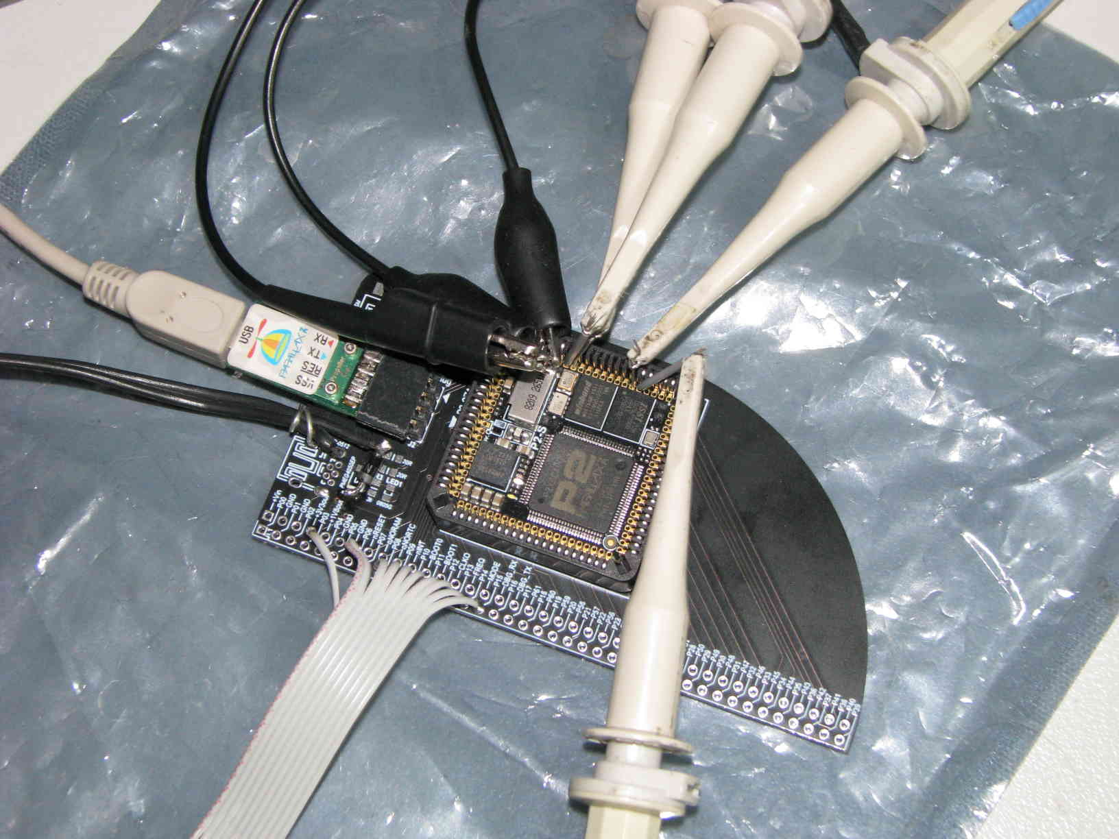
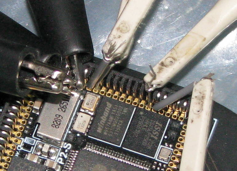
Dirty probes!
They've had some use and been some places. Lost two of the ground clips and broken a hook sadly. And Yokogawa don't sell them any longer.
Yep, sysclock/2 is fine right up to crashing from hubRAM errors.
I've now completed all combinations at sysclock/1 - Which turned out to only be CLK registering, RXDAT registering and RXDAT Schmitting. Inverting CLK polarity has no effect on the RAM's responses since transactions are fixed to first rising clock edge after CE goes low. It ignores any half cycles.
Results were all worse than I already had. The posted sysclk/1 example above, that petered out at 330 MHz, is the best result - Registered CLK, Unregistered DAT.
It can still be improved using temperature and voltage management of course.
EDIT: Here's a small amount of cooling. It helps enough to get to 370 MHz sysclock without crashing. The 100% line makes it to 338 MHz. Some improvement. Stepping the voltage up to 1.9 Volts I expect will give a good improvement. I'll need to find a 27k ohm SMD resistor to do that.
clkfreq = 4000000 clkmode = 010005eb DATA_PIN = 48 addpins 7 DQS_PIN = 56 addpins 0 CLK_PIN = 47 addpins 0 CE_PIN = 46 addpins 0 CLK_POL = 0 RX_SCHMITT = 0 TX_REGD = 0 CLK_REGD = 1 CLK_ADV = 0 Data rate = (sysclock/1) Test data length: 100 x 1024 = 102400 bytes Frequency dependent lag compensation Sysclock u0 r0 u1 r1 u2 r2 u3 r3 u4 r4 u5 r5 u6 r6 60 MHz 0% 0% 0% 0% 100% 100% 0% 0% 0% 0% 0% 0% 0% 0% 62 MHz 0% 0% 0% 0% 100% 100% 0% 0% 0% 0% 0% 0% 0% 0% 64 MHz 0% 0% 0% 0% 100% 100% 0% 0% 0% 0% 0% 0% 0% 0% 66 MHz 0% 0% 0% 0% 100% 100% 0% 0% 0% 0% 0% 0% 0% 0% 68 MHz 0% 0% 0% 0% 100% 100% 0% 0% 0% 0% 0% 0% 0% 0% 70 MHz 0% 0% 0% 0% 100% 100% 0% 0% 0% 0% 0% 0% 0% 0% 72 MHz 0% 0% 0% 0% 100% 100% 0% 0% 0% 0% 0% 0% 0% 0% 74 MHz 0% 0% 0% 0% 100% 100% 0% 0% 0% 0% 0% 0% 0% 0% 76 MHz 0% 0% 0% 0% 100% 100% 0% 0% 0% 0% 0% 0% 0% 0% 78 MHz 0% 0% 0% 0% 100% 100% 0% 0% 0% 0% 0% 0% 0% 0% 80 MHz 0% 0% 0% 0% 100% 100% 0% 0% 0% 0% 0% 0% 0% 0% 82 MHz 0% 0% 0% 0% 100% 100% 0% 0% 0% 0% 0% 0% 0% 0% 84 MHz 0% 0% 0% 0% 100% 100% 0% 0% 0% 0% 0% 0% 0% 0% 86 MHz 0% 0% 0% 0% 100% 100% 0% 0% 0% 0% 0% 0% 0% 0% 88 MHz 0% 0% 0% 0% 100% 100% 0% 0% 0% 0% 0% 0% 0% 0% 90 MHz 0% 0% 0% 0% 100% 100% 0% 0% 0% 0% 0% 0% 0% 0% 92 MHz 0% 0% 0% 0% 100% 100% 0% 0% 0% 0% 0% 0% 0% 0% 94 MHz 0% 0% 0% 0% 100% 100% 0% 0% 0% 0% 0% 0% 0% 0% 96 MHz 0% 0% 0% 0% 100% 100% 0% 0% 0% 0% 0% 0% 0% 0% 98 MHz 0% 0% 0% 0% 100% 100% 0% 0% 0% 0% 0% 0% 0% 0% 100 MHz 0% 0% 0% 0% 100% 100% 0% 0% 0% 0% 0% 0% 0% 0% 102 MHz 0% 0% 0% 0% 100% 100% 0% 0% 0% 0% 0% 0% 0% 0% 104 MHz 0% 0% 0% 0% 100% 100% 0% 0% 0% 0% 0% 0% 0% 0% 106 MHz 0% 0% 0% 0% 100% 100% 0% 0% 0% 0% 0% 0% 0% 0% 108 MHz 0% 0% 0% 0% 100% 100% 0% 0% 0% 0% 0% 0% 0% 0% 110 MHz 0% 0% 0% 0% 100% 100% 0% 0% 0% 0% 0% 0% 0% 0% 112 MHz 0% 0% 0% 0% 100% 100% 0% 0% 0% 0% 0% 0% 0% 0% 114 MHz 0% 0% 0% 0% 100% 100% 0% 0% 0% 0% 0% 0% 0% 0% 116 MHz 0% 0% 0% 0% 100% 100% 0% 0% 0% 0% 0% 0% 0% 0% 118 MHz 0% 0% 0% 0% 96% 100% 0% 0% 0% 0% 0% 0% 0% 0% 120 MHz 0% 0% 0% 0% 22% 100% 0% 0% 0% 0% 0% 0% 0% 0% 122 MHz 0% 0% 0% 0% 0% 100% 0% 0% 0% 0% 0% 0% 0% 0% 124 MHz 0% 0% 0% 0% 0% 100% 0% 0% 0% 0% 0% 0% 0% 0% 126 MHz 0% 0% 0% 0% 0% 100% 0% 0% 0% 0% 0% 0% 0% 0% 128 MHz 0% 0% 0% 0% 0% 100% 49% 0% 0% 0% 0% 0% 0% 0% 130 MHz 0% 0% 0% 0% 0% 100% 100% 0% 0% 0% 0% 0% 0% 0% 132 MHz 0% 0% 0% 0% 0% 100% 100% 0% 0% 0% 0% 0% 0% 0% 134 MHz 0% 0% 0% 0% 0% 100% 100% 0% 0% 0% 0% 0% 0% 0% 136 MHz 0% 0% 0% 0% 0% 100% 100% 0% 0% 0% 0% 0% 0% 0% 138 MHz 0% 0% 0% 0% 0% 100% 100% 0% 0% 0% 0% 0% 0% 0% 140 MHz 0% 0% 0% 0% 0% 100% 100% 0% 0% 0% 0% 0% 0% 0% 142 MHz 0% 0% 0% 0% 0% 100% 100% 0% 0% 0% 0% 0% 0% 0% 144 MHz 0% 0% 0% 0% 0% 100% 100% 0% 0% 0% 0% 0% 0% 0% 146 MHz 0% 0% 0% 0% 0% 100% 100% 0% 0% 0% 0% 0% 0% 0% 148 MHz 0% 0% 0% 0% 0% 100% 100% 0% 0% 0% 0% 0% 0% 0% 150 MHz 0% 0% 0% 0% 0% 100% 100% 0% 0% 0% 0% 0% 0% 0% 152 MHz 0% 0% 0% 0% 0% 100% 100% 0% 0% 0% 0% 0% 0% 0% 154 MHz 0% 0% 0% 0% 0% 100% 100% 0% 0% 0% 0% 0% 0% 0% 156 MHz 0% 0% 0% 0% 0% 100% 100% 0% 0% 0% 0% 0% 0% 0% 158 MHz 0% 0% 0% 0% 0% 100% 100% 0% 0% 0% 0% 0% 0% 0% 160 MHz 0% 0% 0% 0% 0% 100% 100% 0% 0% 0% 0% 0% 0% 0% 162 MHz 0% 0% 0% 0% 0% 99% 100% 0% 0% 0% 0% 0% 0% 0% 164 MHz 0% 0% 0% 0% 0% 81% 100% 0% 0% 0% 0% 0% 0% 0% 166 MHz 0% 0% 0% 0% 0% 23% 100% 0% 0% 0% 0% 0% 0% 0% 168 MHz 0% 0% 0% 0% 0% 1% 100% 0% 0% 0% 0% 0% 0% 0% 170 MHz 0% 0% 0% 0% 0% 0% 100% 0% 0% 0% 0% 0% 0% 0% 172 MHz 0% 0% 0% 0% 0% 0% 100% 0% 0% 0% 0% 0% 0% 0% 174 MHz 0% 0% 0% 0% 0% 0% 100% 0% 0% 0% 0% 0% 0% 0% 176 MHz 0% 0% 0% 0% 0% 0% 100% 0% 0% 0% 0% 0% 0% 0% 178 MHz 0% 0% 0% 0% 0% 0% 100% 0% 0% 0% 0% 0% 0% 0% 180 MHz 0% 0% 0% 0% 0% 0% 100% 10% 0% 0% 0% 0% 0% 0% 182 MHz 0% 0% 0% 0% 0% 0% 100% 69% 0% 0% 0% 0% 0% 0% 184 MHz 0% 0% 0% 0% 0% 0% 100% 99% 0% 0% 0% 0% 0% 0% 186 MHz 0% 0% 0% 0% 0% 0% 100% 100% 0% 0% 0% 0% 0% 0% 188 MHz 0% 0% 0% 0% 0% 0% 100% 100% 0% 0% 0% 0% 0% 0% 190 MHz 0% 0% 0% 0% 0% 0% 100% 100% 0% 0% 0% 0% 0% 0% 192 MHz 0% 0% 0% 0% 0% 0% 100% 100% 0% 0% 0% 0% 0% 0% 194 MHz 0% 0% 0% 0% 0% 0% 100% 100% 0% 0% 0% 0% 0% 0% 196 MHz 0% 0% 0% 0% 0% 0% 100% 100% 0% 0% 0% 0% 0% 0% 198 MHz 0% 0% 0% 0% 0% 0% 100% 100% 0% 0% 0% 0% 0% 0% 200 MHz 0% 0% 0% 0% 0% 0% 100% 100% 0% 0% 0% 0% 0% 0% 202 MHz 0% 0% 0% 0% 0% 0% 100% 100% 0% 0% 0% 0% 0% 0% 204 MHz 0% 0% 0% 0% 0% 0% 100% 100% 0% 0% 0% 0% 0% 0% 206 MHz 0% 0% 0% 0% 0% 0% 100% 100% 0% 0% 0% 0% 0% 0% 208 MHz 0% 0% 0% 0% 0% 0% 100% 100% 0% 0% 0% 0% 0% 0% 210 MHz 0% 0% 0% 0% 0% 0% 100% 100% 0% 0% 0% 0% 0% 0% 212 MHz 0% 0% 0% 0% 0% 0% 100% 100% 0% 0% 0% 0% 0% 0% 214 MHz 0% 0% 0% 0% 0% 0% 100% 100% 0% 0% 0% 0% 0% 0% 216 MHz 0% 0% 0% 0% 0% 0% 100% 100% 0% 0% 0% 0% 0% 0% 218 MHz 0% 0% 0% 0% 0% 0% 100% 100% 0% 0% 0% 0% 0% 0% 220 MHz 0% 0% 0% 0% 0% 0% 100% 100% 0% 0% 0% 0% 0% 0% 222 MHz 0% 0% 0% 0% 0% 0% 100% 100% 0% 0% 0% 0% 0% 0% 224 MHz 0% 0% 0% 0% 0% 0% 100% 100% 0% 0% 0% 0% 0% 0% 226 MHz 0% 0% 0% 0% 0% 0% 100% 100% 0% 0% 0% 0% 0% 0% 228 MHz 0% 0% 0% 0% 0% 0% 100% 100% 0% 0% 0% 0% 0% 0% 230 MHz 0% 0% 0% 0% 0% 0% 100% 100% 0% 0% 0% 0% 0% 0% 232 MHz 0% 0% 0% 0% 0% 0% 100% 100% 0% 0% 0% 0% 0% 0% 234 MHz 0% 0% 0% 0% 0% 0% 99% 100% 0% 0% 0% 0% 0% 0% 236 MHz 0% 0% 0% 0% 0% 0% 96% 100% 0% 0% 0% 0% 0% 0% 238 MHz 0% 0% 0% 0% 0% 0% 73% 100% 0% 0% 0% 0% 0% 0% 240 MHz 0% 0% 0% 0% 0% 0% 19% 100% 0% 0% 0% 0% 0% 0% 242 MHz 0% 0% 0% 0% 0% 0% 2% 100% 0% 0% 0% 0% 0% 0% 244 MHz 0% 0% 0% 0% 0% 0% 0% 100% 0% 0% 0% 0% 0% 0% 246 MHz 0% 0% 0% 0% 0% 0% 0% 100% 0% 0% 0% 0% 0% 0% 248 MHz 0% 0% 0% 0% 0% 0% 0% 100% 0% 0% 0% 0% 0% 0% 250 MHz 0% 0% 0% 0% 0% 0% 0% 100% 0% 0% 0% 0% 0% 0% 252 MHz 0% 0% 0% 0% 0% 0% 0% 100% 0% 0% 0% 0% 0% 0% 254 MHz 0% 0% 0% 0% 0% 0% 0% 100% 5% 0% 0% 0% 0% 0% 256 MHz 0% 0% 0% 0% 0% 0% 0% 100% 46% 0% 0% 0% 0% 0% 258 MHz 0% 0% 0% 0% 0% 0% 0% 100% 93% 0% 0% 0% 0% 0% 260 MHz 0% 0% 0% 0% 0% 0% 0% 100% 99% 0% 0% 0% 0% 0% 262 MHz 0% 0% 0% 0% 0% 0% 0% 100% 100% 0% 0% 0% 0% 0% 264 MHz 0% 0% 0% 0% 0% 0% 0% 100% 100% 0% 0% 0% 0% 0% 266 MHz 0% 0% 0% 0% 0% 0% 0% 100% 100% 0% 0% 0% 0% 0% 268 MHz 0% 0% 0% 0% 0% 0% 0% 100% 100% 0% 0% 0% 0% 0% 270 MHz 0% 0% 0% 0% 0% 0% 0% 100% 100% 0% 0% 0% 0% 0% 272 MHz 0% 0% 0% 0% 0% 0% 0% 100% 100% 0% 0% 0% 0% 0% 274 MHz 0% 0% 0% 0% 0% 0% 0% 100% 100% 0% 0% 0% 0% 0% 276 MHz 0% 0% 0% 0% 0% 0% 0% 100% 100% 0% 0% 0% 0% 0% 278 MHz 0% 0% 0% 0% 0% 0% 0% 100% 100% 0% 0% 0% 0% 0% 280 MHz 0% 0% 0% 0% 0% 0% 0% 100% 100% 0% 0% 0% 0% 0% 282 MHz 0% 0% 0% 0% 0% 0% 0% 100% 100% 0% 0% 0% 0% 0% 284 MHz 0% 0% 0% 0% 0% 0% 0% 100% 100% 0% 0% 0% 0% 0% 286 MHz 0% 0% 0% 0% 0% 0% 0% 100% 100% 0% 0% 0% 0% 0% 288 MHz 0% 0% 0% 0% 0% 0% 0% 100% 100% 0% 0% 0% 0% 0% 290 MHz 0% 0% 0% 0% 0% 0% 0% 100% 100% 0% 0% 0% 0% 0% 292 MHz 0% 0% 0% 0% 0% 0% 0% 100% 100% 0% 0% 0% 0% 0% 294 MHz 0% 0% 0% 0% 0% 0% 0% 100% 100% 0% 0% 0% 0% 0% 296 MHz 0% 0% 0% 0% 0% 0% 0% 100% 100% 0% 0% 0% 0% 0% 298 MHz 0% 0% 0% 0% 0% 0% 0% 100% 100% 0% 0% 0% 0% 0% 300 MHz 0% 0% 0% 0% 0% 0% 0% 100% 100% 0% 0% 0% 0% 0% 302 MHz 0% 0% 0% 0% 0% 0% 0% 100% 100% 0% 0% 0% 0% 0% 304 MHz 0% 0% 0% 0% 0% 0% 0% 100% 100% 0% 0% 0% 0% 0% 306 MHz 0% 0% 0% 0% 0% 0% 0% 100% 100% 0% 0% 0% 0% 0% 308 MHz 0% 0% 0% 0% 0% 0% 0% 100% 100% 0% 0% 0% 0% 0% 310 MHz 0% 0% 0% 0% 0% 0% 0% 99% 100% 0% 0% 0% 0% 0% 312 MHz 0% 0% 0% 0% 0% 0% 0% 99% 100% 0% 0% 0% 0% 0% 314 MHz 0% 0% 0% 0% 0% 0% 0% 99% 100% 0% 0% 0% 0% 0% 316 MHz 0% 0% 0% 0% 0% 0% 0% 98% 100% 0% 0% 0% 0% 0% 318 MHz 0% 0% 0% 0% 0% 0% 0% 96% 100% 0% 0% 0% 0% 0% 320 MHz 0% 0% 0% 0% 0% 0% 0% 89% 100% 0% 0% 0% 0% 0% 322 MHz 0% 0% 0% 0% 0% 0% 0% 77% 100% 0% 0% 0% 0% 0% 324 MHz 0% 0% 0% 0% 0% 0% 0% 60% 100% 0% 0% 0% 0% 0% 326 MHz 0% 0% 0% 0% 0% 0% 0% 40% 100% 0% 0% 0% 0% 0% 328 MHz 0% 0% 0% 0% 0% 0% 0% 21% 100% 0% 0% 0% 0% 0% 330 MHz 0% 0% 0% 0% 0% 0% 0% 10% 100% 0% 0% 0% 0% 0% 332 MHz 0% 0% 0% 0% 0% 0% 0% 5% 100% 0% 0% 0% 0% 0% 334 MHz 0% 0% 0% 0% 0% 0% 0% 2% 100% 0% 0% 0% 0% 0% 336 MHz 0% 0% 0% 0% 0% 0% 0% 1% 100% 0% 0% 0% 0% 0% 338 MHz 0% 0% 0% 0% 0% 0% 0% 0% 100% 0% 0% 0% 0% 0% 340 MHz 0% 0% 0% 0% 0% 0% 0% 0% 99% 0% 0% 0% 0% 0% 342 MHz 0% 0% 0% 0% 0% 0% 0% 0% 99% 0% 0% 0% 0% 0% 344 MHz 0% 0% 0% 0% 0% 0% 0% 0% 99% 0% 0% 0% 0% 0% 346 MHz 0% 0% 0% 0% 0% 0% 0% 0% 97% 0% 0% 0% 0% 0% 348 MHz 0% 0% 0% 0% 0% 0% 0% 0% 93% 0% 0% 0% 0% 0% 350 MHz 0% 0% 0% 0% 0% 0% 0% 0% 82% 0% 0% 0% 0% 0% 352 MHz 0% 0% 0% 0% 0% 0% 0% 0% 67% 0% 0% 0% 0% 0% 354 MHz 0% 0% 0% 0% 0% 0% 0% 0% 49% 0% 0% 0% 0% 0% 356 MHz 0% 0% 0% 0% 0% 0% 0% 0% 30% 3% 0% 0% 0% 0% 358 MHz 0% 0% 0% 0% 0% 0% 0% 0% 15% 10% 0% 0% 0% 0% 360 MHz 0% 0% 0% 0% 0% 0% 0% 0% 5% 12% 0% 0% 0% 0% 362 MHz 0% 0% 0% 0% 0% 0% 0% 0% 1% 7% 0% 0% 0% 0% 364 MHz 0% 0% 0% 0% 0% 0% 0% 0% 0% 0% 0% 0% 0% 0% 366 MHz 0% 0% 0% 0% 0% 0% 0% 0% 0% 0% 0% 0% 0% 0% 368 MHz 0% 0% 0% 0% 0% 0% 0% 0% 0% 0% 0% 0% 0% 0% 370 MHz 0% 0% 0% 0% 0% 0% 0% 0% 0% 0% 0% 1% 0% 0% Sysclock u0 r0 u1 r1 u2 r2 u3 r3 u4 r4 u5 r5 u6 r6A run at 65 degC ambient, an approximation of running with some compute load. It achieves 340 MHz before crashing. RAM 100% reaches to 318 MHz.
DATA_PIN = 48 addpins 7 DQS_PIN = 56 addpins 0 CLK_PIN = 47 addpins 0 CE_PIN = 46 addpins 0 CLK_POL = 0 RX_SCHMITT = 0 TX_REGD = 0 CLK_REGD = 1 CLK_ADV = 0 Data rate = (sysclock/1) Test data length: 100 x 1024 = 102400 bytes Frequency dependent lag compensation Sysclock u0 r0 u1 r1 u2 r2 u3 r3 u4 r4 u5 r5 u6 r6 60 MHz 0% 0% 0% 0% 100% 100% 0% 0% 0% 0% 0% 0% 0% 0% 62 MHz 0% 0% 0% 0% 100% 100% 0% 0% 0% 0% 0% 0% 0% 0% 64 MHz 0% 0% 0% 0% 100% 100% 0% 0% 0% 0% 0% 0% 0% 0% 66 MHz 0% 0% 0% 0% 100% 100% 0% 0% 0% 0% 0% 0% 0% 0% 68 MHz 0% 0% 0% 0% 100% 100% 0% 0% 0% 0% 0% 0% 0% 0% 70 MHz 0% 0% 0% 0% 100% 100% 0% 0% 0% 0% 0% 0% 0% 0% 72 MHz 0% 0% 0% 0% 100% 100% 0% 0% 0% 0% 0% 0% 0% 0% 74 MHz 0% 0% 0% 0% 100% 100% 0% 0% 0% 0% 0% 0% 0% 0% 76 MHz 0% 0% 0% 0% 100% 100% 0% 0% 0% 0% 0% 0% 0% 0% 78 MHz 0% 0% 0% 0% 100% 100% 0% 0% 0% 0% 0% 0% 0% 0% 80 MHz 0% 0% 0% 0% 100% 100% 0% 0% 0% 0% 0% 0% 0% 0% 82 MHz 0% 0% 0% 0% 100% 100% 0% 0% 0% 0% 0% 0% 0% 0% 84 MHz 0% 0% 0% 0% 100% 100% 0% 0% 0% 0% 0% 0% 0% 0% 86 MHz 0% 0% 0% 0% 100% 100% 0% 0% 0% 0% 0% 0% 0% 0% 88 MHz 0% 0% 0% 0% 100% 100% 0% 0% 0% 0% 0% 0% 0% 0% 90 MHz 0% 0% 0% 0% 100% 100% 0% 0% 0% 0% 0% 0% 0% 0% 92 MHz 0% 0% 0% 0% 100% 100% 0% 0% 0% 0% 0% 0% 0% 0% 94 MHz 0% 0% 0% 0% 100% 100% 0% 0% 0% 0% 0% 0% 0% 0% 96 MHz 0% 0% 0% 0% 100% 100% 0% 0% 0% 0% 0% 0% 0% 0% 98 MHz 0% 0% 0% 0% 100% 100% 0% 0% 0% 0% 0% 0% 0% 0% 100 MHz 0% 0% 0% 0% 100% 100% 0% 0% 0% 0% 0% 0% 0% 0% 102 MHz 0% 0% 0% 0% 100% 100% 0% 0% 0% 0% 0% 0% 0% 0% 104 MHz 0% 0% 0% 0% 100% 100% 0% 0% 0% 0% 0% 0% 0% 0% 106 MHz 0% 0% 0% 0% 100% 100% 0% 0% 0% 0% 0% 0% 0% 0% 108 MHz 0% 0% 0% 0% 100% 100% 0% 0% 0% 0% 0% 0% 0% 0% 110 MHz 0% 0% 0% 0% 96% 100% 0% 0% 0% 0% 0% 0% 0% 0% 112 MHz 0% 0% 0% 0% 14% 100% 0% 0% 0% 0% 0% 0% 0% 0% 114 MHz 0% 0% 0% 0% 0% 100% 0% 0% 0% 0% 0% 0% 0% 0% 116 MHz 0% 0% 0% 0% 0% 100% 0% 0% 0% 0% 0% 0% 0% 0% 118 MHz 0% 0% 0% 0% 0% 100% 4% 0% 0% 0% 0% 0% 0% 0% 120 MHz 0% 0% 0% 0% 0% 100% 98% 0% 0% 0% 0% 0% 0% 0% 122 MHz 0% 0% 0% 0% 0% 100% 100% 0% 0% 0% 0% 0% 0% 0% 124 MHz 0% 0% 0% 0% 0% 100% 100% 0% 0% 0% 0% 0% 0% 0% 126 MHz 0% 0% 0% 0% 0% 100% 100% 0% 0% 0% 0% 0% 0% 0% 128 MHz 0% 0% 0% 0% 0% 100% 100% 0% 0% 0% 0% 0% 0% 0% 130 MHz 0% 0% 0% 0% 0% 100% 100% 0% 0% 0% 0% 0% 0% 0% 132 MHz 0% 0% 0% 0% 0% 100% 100% 0% 0% 0% 0% 0% 0% 0% 134 MHz 0% 0% 0% 0% 0% 100% 100% 0% 0% 0% 0% 0% 0% 0% 136 MHz 0% 0% 0% 0% 0% 100% 100% 0% 0% 0% 0% 0% 0% 0% 138 MHz 0% 0% 0% 0% 0% 100% 100% 0% 0% 0% 0% 0% 0% 0% 140 MHz 0% 0% 0% 0% 0% 100% 100% 0% 0% 0% 0% 0% 0% 0% 142 MHz 0% 0% 0% 0% 0% 100% 100% 0% 0% 0% 0% 0% 0% 0% 144 MHz 0% 0% 0% 0% 0% 100% 100% 0% 0% 0% 0% 0% 0% 0% 146 MHz 0% 0% 0% 0% 0% 100% 100% 0% 0% 0% 0% 0% 0% 0% 148 MHz 0% 0% 0% 0% 0% 100% 100% 0% 0% 0% 0% 0% 0% 0% 150 MHz 0% 0% 0% 0% 0% 99% 100% 0% 0% 0% 0% 0% 0% 0% 152 MHz 0% 0% 0% 0% 0% 85% 100% 0% 0% 0% 0% 0% 0% 0% 154 MHz 0% 0% 0% 0% 0% 33% 100% 0% 0% 0% 0% 0% 0% 0% 156 MHz 0% 0% 0% 0% 0% 2% 100% 0% 0% 0% 0% 0% 0% 0% 158 MHz 0% 0% 0% 0% 0% 0% 100% 0% 0% 0% 0% 0% 0% 0% 160 MHz 0% 0% 0% 0% 0% 0% 100% 0% 0% 0% 0% 0% 0% 0% 162 MHz 0% 0% 0% 0% 0% 0% 100% 0% 0% 0% 0% 0% 0% 0% 164 MHz 0% 0% 0% 0% 0% 0% 100% 0% 0% 0% 0% 0% 0% 0% 166 MHz 0% 0% 0% 0% 0% 0% 100% 0% 0% 0% 0% 0% 0% 0% 168 MHz 0% 0% 0% 0% 0% 0% 100% 29% 0% 0% 0% 0% 0% 0% 170 MHz 0% 0% 0% 0% 0% 0% 100% 91% 0% 0% 0% 0% 0% 0% 172 MHz 0% 0% 0% 0% 0% 0% 100% 100% 0% 0% 0% 0% 0% 0% 174 MHz 0% 0% 0% 0% 0% 0% 100% 100% 0% 0% 0% 0% 0% 0% 176 MHz 0% 0% 0% 0% 0% 0% 100% 100% 0% 0% 0% 0% 0% 0% 178 MHz 0% 0% 0% 0% 0% 0% 100% 100% 0% 0% 0% 0% 0% 0% 180 MHz 0% 0% 0% 0% 0% 0% 100% 100% 0% 0% 0% 0% 0% 0% 182 MHz 0% 0% 0% 0% 0% 0% 100% 100% 0% 0% 0% 0% 0% 0% 184 MHz 0% 0% 0% 0% 0% 0% 100% 100% 0% 0% 0% 0% 0% 0% 186 MHz 0% 0% 0% 0% 0% 0% 100% 100% 0% 0% 0% 0% 0% 0% 188 MHz 0% 0% 0% 0% 0% 0% 100% 100% 0% 0% 0% 0% 0% 0% 190 MHz 0% 0% 0% 0% 0% 0% 100% 100% 0% 0% 0% 0% 0% 0% 192 MHz 0% 0% 0% 0% 0% 0% 100% 100% 0% 0% 0% 0% 0% 0% 194 MHz 0% 0% 0% 0% 0% 0% 100% 100% 0% 0% 0% 0% 0% 0% 196 MHz 0% 0% 0% 0% 0% 0% 100% 100% 0% 0% 0% 0% 0% 0% 198 MHz 0% 0% 0% 0% 0% 0% 100% 100% 0% 0% 0% 0% 0% 0% 200 MHz 0% 0% 0% 0% 0% 0% 100% 100% 0% 0% 0% 0% 0% 0% 202 MHz 0% 0% 0% 0% 0% 0% 100% 100% 0% 0% 0% 0% 0% 0% 204 MHz 0% 0% 0% 0% 0% 0% 100% 100% 0% 0% 0% 0% 0% 0% 206 MHz 0% 0% 0% 0% 0% 0% 100% 100% 0% 0% 0% 0% 0% 0% 208 MHz 0% 0% 0% 0% 0% 0% 100% 100% 0% 0% 0% 0% 0% 0% 210 MHz 0% 0% 0% 0% 0% 0% 100% 100% 0% 0% 0% 0% 0% 0% 212 MHz 0% 0% 0% 0% 0% 0% 100% 100% 0% 0% 0% 0% 0% 0% 214 MHz 0% 0% 0% 0% 0% 0% 100% 100% 0% 0% 0% 0% 0% 0% 216 MHz 0% 0% 0% 0% 0% 0% 99% 100% 0% 0% 0% 0% 0% 0% 218 MHz 0% 0% 0% 0% 0% 0% 99% 100% 0% 0% 0% 0% 0% 0% 220 MHz 0% 0% 0% 0% 0% 0% 94% 100% 0% 0% 0% 0% 0% 0% 222 MHz 0% 0% 0% 0% 0% 0% 63% 100% 0% 0% 0% 0% 0% 0% 224 MHz 0% 0% 0% 0% 0% 0% 13% 100% 0% 0% 0% 0% 0% 0% 226 MHz 0% 0% 0% 0% 0% 0% 0% 100% 0% 0% 0% 0% 0% 0% 228 MHz 0% 0% 0% 0% 0% 0% 0% 100% 0% 0% 0% 0% 0% 0% 230 MHz 0% 0% 0% 0% 0% 0% 0% 100% 0% 0% 0% 0% 0% 0% 232 MHz 0% 0% 0% 0% 0% 0% 0% 100% 0% 0% 0% 0% 0% 0% 234 MHz 0% 0% 0% 0% 0% 0% 0% 100% 0% 0% 0% 0% 0% 0% 236 MHz 0% 0% 0% 0% 0% 0% 0% 100% 3% 0% 0% 0% 0% 0% 238 MHz 0% 0% 0% 0% 0% 0% 0% 100% 62% 0% 0% 0% 0% 0% 240 MHz 0% 0% 0% 0% 0% 0% 0% 100% 99% 0% 0% 0% 0% 0% 242 MHz 0% 0% 0% 0% 0% 0% 0% 100% 100% 0% 0% 0% 0% 0% 244 MHz 0% 0% 0% 0% 0% 0% 0% 100% 100% 0% 0% 0% 0% 0% 246 MHz 0% 0% 0% 0% 0% 0% 0% 100% 100% 0% 0% 0% 0% 0% 248 MHz 0% 0% 0% 0% 0% 0% 0% 100% 100% 0% 0% 0% 0% 0% 250 MHz 0% 0% 0% 0% 0% 0% 0% 100% 100% 0% 0% 0% 0% 0% 252 MHz 0% 0% 0% 0% 0% 0% 0% 100% 100% 0% 0% 0% 0% 0% 254 MHz 0% 0% 0% 0% 0% 0% 0% 100% 100% 0% 0% 0% 0% 0% 256 MHz 0% 0% 0% 0% 0% 0% 0% 100% 100% 0% 0% 0% 0% 0% 258 MHz 0% 0% 0% 0% 0% 0% 0% 100% 100% 0% 0% 0% 0% 0% 260 MHz 0% 0% 0% 0% 0% 0% 0% 100% 100% 0% 0% 0% 0% 0% 262 MHz 0% 0% 0% 0% 0% 0% 0% 100% 100% 0% 0% 0% 0% 0% 264 MHz 0% 0% 0% 0% 0% 0% 0% 100% 100% 0% 0% 0% 0% 0% 266 MHz 0% 0% 0% 0% 0% 0% 0% 100% 100% 0% 0% 0% 0% 0% 268 MHz 0% 0% 0% 0% 0% 0% 0% 100% 100% 0% 0% 0% 0% 0% 270 MHz 0% 0% 0% 0% 0% 0% 0% 100% 100% 0% 0% 0% 0% 0% 272 MHz 0% 0% 0% 0% 0% 0% 0% 100% 100% 0% 0% 0% 0% 0% 274 MHz 0% 0% 0% 0% 0% 0% 0% 100% 100% 0% 0% 0% 0% 0% 276 MHz 0% 0% 0% 0% 0% 0% 0% 100% 100% 0% 0% 0% 0% 0% 278 MHz 0% 0% 0% 0% 0% 0% 0% 100% 100% 0% 0% 0% 0% 0% 280 MHz 0% 0% 0% 0% 0% 0% 0% 100% 100% 0% 0% 0% 0% 0% 282 MHz 0% 0% 0% 0% 0% 0% 0% 100% 100% 0% 0% 0% 0% 0% 284 MHz 0% 0% 0% 0% 0% 0% 0% 100% 100% 0% 0% 0% 0% 0% 286 MHz 0% 0% 0% 0% 0% 0% 0% 100% 100% 0% 0% 0% 0% 0% 288 MHz 0% 0% 0% 0% 0% 0% 0% 100% 100% 0% 0% 0% 0% 0% 290 MHz 0% 0% 0% 0% 0% 0% 0% 99% 100% 0% 0% 0% 0% 0% 292 MHz 0% 0% 0% 0% 0% 0% 0% 99% 100% 0% 0% 0% 0% 0% 294 MHz 0% 0% 0% 0% 0% 0% 0% 99% 100% 0% 0% 0% 0% 0% 296 MHz 0% 0% 0% 0% 0% 0% 0% 97% 100% 0% 0% 0% 0% 0% 298 MHz 0% 0% 0% 0% 0% 0% 0% 92% 100% 0% 0% 0% 0% 0% 300 MHz 0% 0% 0% 0% 0% 0% 0% 82% 100% 0% 0% 0% 0% 0% 302 MHz 0% 0% 0% 0% 0% 0% 0% 66% 100% 0% 0% 0% 0% 0% 304 MHz 0% 0% 0% 0% 0% 0% 0% 44% 100% 0% 0% 0% 0% 0% 306 MHz 0% 0% 0% 0% 0% 0% 0% 25% 100% 0% 0% 0% 0% 0% 308 MHz 0% 0% 0% 0% 0% 0% 0% 11% 100% 0% 0% 0% 0% 0% 310 MHz 0% 0% 0% 0% 0% 0% 0% 4% 100% 0% 0% 0% 0% 0% 312 MHz 0% 0% 0% 0% 0% 0% 0% 1% 100% 0% 0% 0% 0% 0% 314 MHz 0% 0% 0% 0% 0% 0% 0% 0% 100% 0% 0% 0% 0% 0% 316 MHz 0% 0% 0% 0% 0% 0% 0% 0% 100% 0% 0% 0% 0% 0% 318 MHz 0% 0% 0% 0% 0% 0% 0% 0% 99% 0% 0% 0% 0% 0% 320 MHz 0% 0% 0% 0% 0% 0% 0% 0% 99% 0% 0% 0% 0% 0% 322 MHz 0% 0% 0% 0% 0% 0% 0% 0% 99% 0% 0% 0% 0% 0% 324 MHz 0% 0% 0% 0% 0% 0% 0% 0% 95% 0% 0% 0% 0% 0% 326 MHz 0% 0% 0% 0% 0% 0% 0% 0% 87% 0% 0% 0% 0% 0% 328 MHz 0% 0% 0% 0% 0% 0% 0% 0% 70% 0% 0% 0% 0% 0% 330 MHz 0% 0% 0% 0% 0% 0% 0% 0% 49% 0% 0% 0% 0% 0% 332 MHz 0% 0% 0% 0% 0% 0% 0% 0% 26% 4% 0% 0% 0% 0% 334 MHz 0% 0% 0% 0% 0% 0% 0% 0% 11% 8% 0% 0% 0% 0% 336 MHz 0% 0% 0% 0% 0% 0% 0% 0% 2% 2% 0% 0% 0% 0% 338 MHz 0% 0% 0% 0% 0% 0% 0% 0% 0% 0% 0% 0% 0% 0% 340 MHz 0% 0% 0% 0% 0% 0% 0% 0% 0% 0% 0% 0% 0% 0% 342 MHz 0% 0% 0% 0% 0% 0% 0% 0% 0% 0% 0% 1% 0% 0%And at 95 degC, for estimated heavy compute, we get crash at 326 MHz and RAM 100% reaches 300 MHz.
DATA_PIN = 48 addpins 7 DQS_PIN = 56 addpins 0 CLK_PIN = 47 addpins 0 CE_PIN = 46 addpins 0 CLK_POL = 0 RX_SCHMITT = 0 TX_REGD = 0 CLK_REGD = 1 CLK_ADV = 0 Data rate = (sysclock/1) Test data length: 100 x 1024 = 102400 bytes Frequency dependent lag compensation Sysclock u0 r0 u1 r1 u2 r2 u3 r3 u4 r4 u5 r5 u6 r6 60 MHz 0% 0% 0% 0% 100% 100% 0% 0% 0% 0% 0% 0% 0% 0% 62 MHz 0% 0% 0% 0% 100% 100% 0% 0% 0% 0% 0% 0% 0% 0% 64 MHz 0% 0% 0% 0% 100% 100% 0% 0% 0% 0% 0% 0% 0% 0% 66 MHz 0% 0% 0% 0% 100% 100% 0% 0% 0% 0% 0% 0% 0% 0% 68 MHz 0% 0% 0% 0% 100% 100% 0% 0% 0% 0% 0% 0% 0% 0% 70 MHz 0% 0% 0% 0% 100% 100% 0% 0% 0% 0% 0% 0% 0% 0% 72 MHz 0% 0% 0% 0% 100% 100% 0% 0% 0% 0% 0% 0% 0% 0% 74 MHz 0% 0% 0% 0% 100% 100% 0% 0% 0% 0% 0% 0% 0% 0% 76 MHz 0% 0% 0% 0% 100% 100% 0% 0% 0% 0% 0% 0% 0% 0% 78 MHz 0% 0% 0% 0% 100% 100% 0% 0% 0% 0% 0% 0% 0% 0% 80 MHz 0% 0% 0% 0% 100% 100% 0% 0% 0% 0% 0% 0% 0% 0% 82 MHz 0% 0% 0% 0% 100% 100% 0% 0% 0% 0% 0% 0% 0% 0% 84 MHz 0% 0% 0% 0% 100% 100% 0% 0% 0% 0% 0% 0% 0% 0% 86 MHz 0% 0% 0% 0% 100% 100% 0% 0% 0% 0% 0% 0% 0% 0% 88 MHz 0% 0% 0% 0% 100% 100% 0% 0% 0% 0% 0% 0% 0% 0% 90 MHz 0% 0% 0% 0% 100% 100% 0% 0% 0% 0% 0% 0% 0% 0% 92 MHz 0% 0% 0% 0% 100% 100% 0% 0% 0% 0% 0% 0% 0% 0% 94 MHz 0% 0% 0% 0% 100% 100% 0% 0% 0% 0% 0% 0% 0% 0% 96 MHz 0% 0% 0% 0% 100% 100% 0% 0% 0% 0% 0% 0% 0% 0% 98 MHz 0% 0% 0% 0% 100% 100% 0% 0% 0% 0% 0% 0% 0% 0% 100 MHz 0% 0% 0% 0% 100% 100% 0% 0% 0% 0% 0% 0% 0% 0% 102 MHz 0% 0% 0% 0% 100% 100% 0% 0% 0% 0% 0% 0% 0% 0% 104 MHz 0% 0% 0% 0% 99% 100% 0% 0% 0% 0% 0% 0% 0% 0% 106 MHz 0% 0% 0% 0% 44% 100% 0% 0% 0% 0% 0% 0% 0% 0% 108 MHz 0% 0% 0% 0% 0% 100% 0% 0% 0% 0% 0% 0% 0% 0% 110 MHz 0% 0% 0% 0% 0% 100% 0% 0% 0% 0% 0% 0% 0% 0% 112 MHz 0% 0% 0% 0% 0% 100% 2% 0% 0% 0% 0% 0% 0% 0% 114 MHz 0% 0% 0% 0% 0% 100% 97% 0% 0% 0% 0% 0% 0% 0% 116 MHz 0% 0% 0% 0% 0% 100% 100% 0% 0% 0% 0% 0% 0% 0% 118 MHz 0% 0% 0% 0% 0% 100% 100% 0% 0% 0% 0% 0% 0% 0% 120 MHz 0% 0% 0% 0% 0% 100% 100% 0% 0% 0% 0% 0% 0% 0% 122 MHz 0% 0% 0% 0% 0% 100% 100% 0% 0% 0% 0% 0% 0% 0% 124 MHz 0% 0% 0% 0% 0% 100% 100% 0% 0% 0% 0% 0% 0% 0% 126 MHz 0% 0% 0% 0% 0% 100% 100% 0% 0% 0% 0% 0% 0% 0% 128 MHz 0% 0% 0% 0% 0% 100% 100% 0% 0% 0% 0% 0% 0% 0% 130 MHz 0% 0% 0% 0% 0% 100% 100% 0% 0% 0% 0% 0% 0% 0% 132 MHz 0% 0% 0% 0% 0% 100% 100% 0% 0% 0% 0% 0% 0% 0% 134 MHz 0% 0% 0% 0% 0% 100% 100% 0% 0% 0% 0% 0% 0% 0% 136 MHz 0% 0% 0% 0% 0% 100% 100% 0% 0% 0% 0% 0% 0% 0% 138 MHz 0% 0% 0% 0% 0% 100% 100% 0% 0% 0% 0% 0% 0% 0% 140 MHz 0% 0% 0% 0% 0% 100% 100% 0% 0% 0% 0% 0% 0% 0% 142 MHz 0% 0% 0% 0% 0% 99% 100% 0% 0% 0% 0% 0% 0% 0% 144 MHz 0% 0% 0% 0% 0% 92% 100% 0% 0% 0% 0% 0% 0% 0% 146 MHz 0% 0% 0% 0% 0% 41% 100% 0% 0% 0% 0% 0% 0% 0% 148 MHz 0% 0% 0% 0% 0% 3% 100% 0% 0% 0% 0% 0% 0% 0% 150 MHz 0% 0% 0% 0% 0% 0% 100% 0% 0% 0% 0% 0% 0% 0% 152 MHz 0% 0% 0% 0% 0% 0% 100% 0% 0% 0% 0% 0% 0% 0% 154 MHz 0% 0% 0% 0% 0% 0% 100% 0% 0% 0% 0% 0% 0% 0% 156 MHz 0% 0% 0% 0% 0% 0% 100% 0% 0% 0% 0% 0% 0% 0% 158 MHz 0% 0% 0% 0% 0% 0% 100% 1% 0% 0% 0% 0% 0% 0% 160 MHz 0% 0% 0% 0% 0% 0% 100% 45% 0% 0% 0% 0% 0% 0% 162 MHz 0% 0% 0% 0% 0% 0% 100% 96% 0% 0% 0% 0% 0% 0% 164 MHz 0% 0% 0% 0% 0% 0% 100% 100% 0% 0% 0% 0% 0% 0% 166 MHz 0% 0% 0% 0% 0% 0% 100% 100% 0% 0% 0% 0% 0% 0% 168 MHz 0% 0% 0% 0% 0% 0% 100% 100% 0% 0% 0% 0% 0% 0% 170 MHz 0% 0% 0% 0% 0% 0% 100% 100% 0% 0% 0% 0% 0% 0% 172 MHz 0% 0% 0% 0% 0% 0% 100% 100% 0% 0% 0% 0% 0% 0% 174 MHz 0% 0% 0% 0% 0% 0% 100% 100% 0% 0% 0% 0% 0% 0% 176 MHz 0% 0% 0% 0% 0% 0% 100% 100% 0% 0% 0% 0% 0% 0% 178 MHz 0% 0% 0% 0% 0% 0% 100% 100% 0% 0% 0% 0% 0% 0% 180 MHz 0% 0% 0% 0% 0% 0% 100% 100% 0% 0% 0% 0% 0% 0% 182 MHz 0% 0% 0% 0% 0% 0% 100% 100% 0% 0% 0% 0% 0% 0% 184 MHz 0% 0% 0% 0% 0% 0% 100% 100% 0% 0% 0% 0% 0% 0% 186 MHz 0% 0% 0% 0% 0% 0% 100% 100% 0% 0% 0% 0% 0% 0% 188 MHz 0% 0% 0% 0% 0% 0% 100% 100% 0% 0% 0% 0% 0% 0% 190 MHz 0% 0% 0% 0% 0% 0% 100% 100% 0% 0% 0% 0% 0% 0% 192 MHz 0% 0% 0% 0% 0% 0% 100% 100% 0% 0% 0% 0% 0% 0% 194 MHz 0% 0% 0% 0% 0% 0% 100% 100% 0% 0% 0% 0% 0% 0% 196 MHz 0% 0% 0% 0% 0% 0% 100% 100% 0% 0% 0% 0% 0% 0% 198 MHz 0% 0% 0% 0% 0% 0% 100% 100% 0% 0% 0% 0% 0% 0% 200 MHz 0% 0% 0% 0% 0% 0% 100% 100% 0% 0% 0% 0% 0% 0% 202 MHz 0% 0% 0% 0% 0% 0% 100% 100% 0% 0% 0% 0% 0% 0% 204 MHz 0% 0% 0% 0% 0% 0% 100% 100% 0% 0% 0% 0% 0% 0% 206 MHz 0% 0% 0% 0% 0% 0% 99% 100% 0% 0% 0% 0% 0% 0% 208 MHz 0% 0% 0% 0% 0% 0% 99% 100% 0% 0% 0% 0% 0% 0% 210 MHz 0% 0% 0% 0% 0% 0% 87% 100% 0% 0% 0% 0% 0% 0% 212 MHz 0% 0% 0% 0% 0% 0% 41% 100% 0% 0% 0% 0% 0% 0% 214 MHz 0% 0% 0% 0% 0% 0% 3% 100% 0% 0% 0% 0% 0% 0% 216 MHz 0% 0% 0% 0% 0% 0% 0% 100% 0% 0% 0% 0% 0% 0% 218 MHz 0% 0% 0% 0% 0% 0% 0% 100% 0% 0% 0% 0% 0% 0% 220 MHz 0% 0% 0% 0% 0% 0% 0% 100% 0% 0% 0% 0% 0% 0% 222 MHz 0% 0% 0% 0% 0% 0% 0% 100% 0% 0% 0% 0% 0% 0% 224 MHz 0% 0% 0% 0% 0% 0% 0% 100% 2% 0% 0% 0% 0% 0% 226 MHz 0% 0% 0% 0% 0% 0% 0% 100% 60% 0% 0% 0% 0% 0% 228 MHz 0% 0% 0% 0% 0% 0% 0% 100% 99% 0% 0% 0% 0% 0% 230 MHz 0% 0% 0% 0% 0% 0% 0% 100% 100% 0% 0% 0% 0% 0% 232 MHz 0% 0% 0% 0% 0% 0% 0% 100% 100% 0% 0% 0% 0% 0% 234 MHz 0% 0% 0% 0% 0% 0% 0% 100% 100% 0% 0% 0% 0% 0% 236 MHz 0% 0% 0% 0% 0% 0% 0% 100% 100% 0% 0% 0% 0% 0% 238 MHz 0% 0% 0% 0% 0% 0% 0% 100% 100% 0% 0% 0% 0% 0% 240 MHz 0% 0% 0% 0% 0% 0% 0% 100% 100% 0% 0% 0% 0% 0% 242 MHz 0% 0% 0% 0% 0% 0% 0% 100% 100% 0% 0% 0% 0% 0% 244 MHz 0% 0% 0% 0% 0% 0% 0% 100% 100% 0% 0% 0% 0% 0% 246 MHz 0% 0% 0% 0% 0% 0% 0% 100% 100% 0% 0% 0% 0% 0% 248 MHz 0% 0% 0% 0% 0% 0% 0% 100% 100% 0% 0% 0% 0% 0% 250 MHz 0% 0% 0% 0% 0% 0% 0% 100% 100% 0% 0% 0% 0% 0% 252 MHz 0% 0% 0% 0% 0% 0% 0% 100% 100% 0% 0% 0% 0% 0% 254 MHz 0% 0% 0% 0% 0% 0% 0% 100% 100% 0% 0% 0% 0% 0% 256 MHz 0% 0% 0% 0% 0% 0% 0% 100% 100% 0% 0% 0% 0% 0% 258 MHz 0% 0% 0% 0% 0% 0% 0% 100% 100% 0% 0% 0% 0% 0% 260 MHz 0% 0% 0% 0% 0% 0% 0% 100% 100% 0% 0% 0% 0% 0% 262 MHz 0% 0% 0% 0% 0% 0% 0% 100% 100% 0% 0% 0% 0% 0% 264 MHz 0% 0% 0% 0% 0% 0% 0% 100% 100% 0% 0% 0% 0% 0% 266 MHz 0% 0% 0% 0% 0% 0% 0% 100% 100% 0% 0% 0% 0% 0% 268 MHz 0% 0% 0% 0% 0% 0% 0% 100% 100% 0% 0% 0% 0% 0% 270 MHz 0% 0% 0% 0% 0% 0% 0% 100% 100% 0% 0% 0% 0% 0% 272 MHz 0% 0% 0% 0% 0% 0% 0% 100% 100% 0% 0% 0% 0% 0% 274 MHz 0% 0% 0% 0% 0% 0% 0% 100% 100% 0% 0% 0% 0% 0% 276 MHz 0% 0% 0% 0% 0% 0% 0% 99% 100% 0% 0% 0% 0% 0% 278 MHz 0% 0% 0% 0% 0% 0% 0% 99% 100% 0% 0% 0% 0% 0% 280 MHz 0% 0% 0% 0% 0% 0% 0% 99% 100% 0% 0% 0% 0% 0% 282 MHz 0% 0% 0% 0% 0% 0% 0% 97% 100% 0% 0% 0% 0% 0% 284 MHz 0% 0% 0% 0% 0% 0% 0% 91% 100% 0% 0% 0% 0% 0% 286 MHz 0% 0% 0% 0% 0% 0% 0% 80% 100% 0% 0% 0% 0% 0% 288 MHz 0% 0% 0% 0% 0% 0% 0% 61% 100% 0% 0% 0% 0% 0% 290 MHz 0% 0% 0% 0% 0% 0% 0% 39% 100% 0% 0% 0% 0% 0% 292 MHz 0% 0% 0% 0% 0% 0% 0% 19% 100% 0% 0% 0% 0% 0% 294 MHz 0% 0% 0% 0% 0% 0% 0% 7% 100% 0% 0% 0% 0% 0% 296 MHz 0% 0% 0% 0% 0% 0% 0% 2% 100% 0% 0% 0% 0% 0% 298 MHz 0% 0% 0% 0% 0% 0% 0% 0% 100% 0% 0% 0% 0% 0% 300 MHz 0% 0% 0% 0% 0% 0% 0% 0% 100% 0% 0% 0% 0% 0% 302 MHz 0% 0% 0% 0% 0% 0% 0% 0% 99% 0% 0% 0% 0% 0% 304 MHz 0% 0% 0% 0% 0% 0% 0% 0% 99% 0% 0% 0% 0% 0% 306 MHz 0% 0% 0% 0% 0% 0% 0% 0% 99% 0% 0% 0% 0% 0% 308 MHz 0% 0% 0% 0% 0% 0% 0% 0% 97% 0% 0% 0% 0% 0% 310 MHz 0% 0% 0% 0% 0% 0% 0% 0% 90% 0% 0% 0% 0% 0% 312 MHz 0% 0% 0% 0% 0% 0% 0% 0% 73% 0% 0% 0% 0% 0% 314 MHz 0% 0% 0% 0% 0% 0% 0% 0% 51% 0% 0% 0% 0% 0% 316 MHz 0% 0% 0% 0% 0% 0% 0% 0% 26% 3% 0% 0% 0% 0% 318 MHz 0% 0% 0% 0% 0% 0% 0% 0% 10% 5% 0% 0% 0% 0% 320 MHz 0% 0% 0% 0% 0% 0% 0% 0% 2% 0% 0% 0% 0% 0% 322 MHz 0% 0% 0% 0% 0% 0% 0% 0% 0% 0% 0% 0% 0% 0% 324 MHz 0% 0% 0% 0% 0% 0% 0% 0% 0% 0% 0% 1% 0% 0% 326 MHz 0% 0% 0% 0% 0% 0% 0% 0% 0% 0% 0% 13% 0% 0%Gearing up for P2 Stamp assembly using new PandaPlacer (OpenPNP based).
The Eagle export from the original Altium was very useful here as was able to export the part locations into the OpenPNP software using a ULP.
Just tested placing the P2 chip and it looks good.
The RTC that @knivd picked has some interesting features...
Integrated crystal is nice with such a small package. A lot smaller that the DS one. Says its under vacuum inside. That's interesting... Guess the crystal is moving around in there and doesn't want air stopping it...
Noticed it has a temperature sensor. That could be useful to answer questions about if the Stamp is getting hot when inside a case with little airflow.
The 8 bytes of user RAM is interesting too. For control applications, having something that retains state even after power failure is nice. Have to think about if this has any practical value, when one could just save things to flash or uSD...