In the schematic, Q1 and Q2 look reversed. The Drains (terminal 3) aren't normally put on the supply side. The forward biased ESD diode stood out to me.
EDIT: Never mind, I see they latch on after the diodes conduct. I presume that is some kind of soft-start circuit?
EDIT2: Reading the datasheet, those transistors are good for 5 amps each continuous. Why use two?
Thanks for posting your schematic @knivd . Yes I recognized the reverse voltage protection with that input FET pair. A while back I noticed you had mentioned you could take up to 20V input:
And yes, there are both 3.3V and 1.8V supplies, 2.5A on each rail, and they are also available to feed outside circuits as much as the power budget allows.
Input is in the range 3.6V - 20V.
But the CSD25485F5 FETs seem to list Vgs as -12V max. So be careful with your input voltage when you test. To widen the input voltage range a zener diode can be used between the gate and source to clamp it, with a resistor from gate to ground as shown here: https://components101.com/articles/design-guide-pmos-mosfet-for-reverse-voltage-polarity-protection
If you do find you need a board rev maybe some of this can be added if there is any room (you could share the one circuit over both FET gates). It'd be nice to accept up to 15V or so for automotive type applications and your -20V Vds rated PFET and LTM4622 would allow that voltage and reverse protect it without frying, except for the gate voltage issue.
I have taken great care regarding the thermal challenges. There are a few layers in the PCB with that very purpose and lead the heat out to the carrier board through several ground pins.
With that HyperRAM right there, care to hook a pin to a TV and run one of my emulators? (If you configure to direct boot a ROM, you don't really need input). So far I think the record for any non-Parallax board is running for like 10 minutes before crashing.
If it keeps going over night, you've got a true winner on your hands.
@rogloh said:
To widen the input voltage range a zener diode can be used between the gate and source to clamp it, with a resistor from gate to ground as shown here:
I noted that is built-in to the CSD25485F5. So knivd has that covered to.
@rogloh said:
To widen the input voltage range a zener diode can be used between the gate and source to clamp it, with a resistor from gate to ground as shown here:
I noted that is built-in to the CSD25485F5. So knivd has that covered to.
Curious that the datasheet has Vgs rating at -12V despite that unusual schematic. If we believe the headline numbers, then 12V would be the maximum reverse voltage protection. (Without an external res/dio bleed as suggested).
Ah, I think I see. The protection isn't for Gate input voltage, it's to neuter capacitively coupled drain-gate reverse spikes coming out of the gate back-feeding a gate driver. A Vgs protection as well. Very important for switching/modulating an output load on the drain. EDIT: Grr, no, that's not it completely either. Those are usually zenor (TVS) diodes.
Roger is right, a 20 volt supply will lift Vgs too high.
EDIT2: Just realised Roger's link is using zenors too. And relies on the resistor being of much higher resistance than what would be used in a modulating circuit. I certainly wouldn't use the 100 ohms example. Way too low resistance. Gate capacitance is only 0.5 nF.
@VonSzarvas said:
Curious that the datasheet has Vgs rating at -12V despite that unusual schematic. If we believe the headline numbers, then 12V would be the maximum reverse voltage protection. (Without an external res/dio bleed as suggested).
I think it would also be the maximum input voltage too, not just the reverse limit. When the PFET is turned on, Vgs is also reaching up to -12V if the input is fed by 12V (since the gate is grounded) as there is barely any drop from drain to source. You probably couldn't safely rate the input to 12V with this design without that zener, it's too close to the limit. 5-9V is fine though to begin with, but given the regulator can reach 20V it'd be rather nice to allow something like a 15-20V range (and reverse protect it too).
@rogloh said:
Thanks for posting your schematic @knivd . Yes I recognized the reverse voltage protection with that input FET pair. A while back I noticed you had mentioned you could take up to 20V input:
But the CSD25485F5 FETs seem to list Vgs as -12V max. So be careful with your input voltage when you test. To widen the input voltage range a zener diode can be used between the gate and source to clamp it, with a resistor from gate to ground as shown here:
Ah, yes indeed. Initially there were different transistors there, which I later changed for some reason (price or availability). I have overlooked that detail, but fortunately it should be easy enough to fix it with your suggested solution. I will modify the schematic for the next revision. Until then, up to 12V input, unfortunately
@Wuerfel_21 said:
With that HyperRAM right there, care to hook a pin to a TV and run one of my emulators? (If you configure to direct boot a ROM, you don't really need input). So far I think the record for any non-Parallax board is running for like 10 minutes before crashing.
Happy to do that. Please send further instructions what is needed, and a suggested schematic for connecting. And what to run, of course
@knivd said:
Ah, yes indeed. Initially there were different transistors there, which I later changed for some reason (price or availability). I have overlooked that detail, but fortunately it should be easy enough to fix it with your suggested solution. I will modify the schematic for the next revision. Until then, up to 12V input, unfortunately
Sounds good. When I took a look at your layout it seemed like you'd have a little bit of wiggle room to stack the nearby resistors for free space and you can get Zener diodes in the 0603 size (or just put them underneath the board). For the tiny incremental part cost of a diode+resistor it'd be well worth the improved input voltage range in a following revision.
If you still ultimately plan to make this available I am certainly interested in some of these, and also powering them at 12V with some margin for supply range safety. Looking forward to seeing how well your board turns out and how fast it can be reliably clocked.
p.s. what's the total thickness of this design with top + bottom components fitted? Something ~5mm? I'm looking for low profile. The original P2 Edge board is 5.5mm which could possibly suit. But its bulky connector is a killer.
@rogloh said:
p.s. what's the total thickness of this design with top + bottom components fitted? Something ~5mm? I'm looking for low profile. The original P2 Edge board is 5.5mm which could possibly suit. But its bulky connector is a killer.
The tallest component on the top side is the SD connector - 2.65mm, and on the bottom are only capacitors - 0.5mm. The PCB itself is 1.2mm, so yes - less than 5mm in total, which with an inverted footprint and cutout for the top side (google up and see my ELLO LC1 as a practical realisation of the idea), could give you a pretty thin solution
@Simonius said:
I like the design. How is the analog performance? (ADC/DAC) Would it make any difference if there were additional linear stages in the power supply?
One of the things to be determined with practical use
@Wuerfel_21 said:
With that HyperRAM right there, care to hook a pin to a TV and run one of my emulators? (If you configure to direct boot a ROM, you don't really need input). So far I think the record for any non-Parallax board is running for like 10 minutes before crashing.
Happy to do that. Please send further instructions what is needed, and a suggested schematic for connecting. And what to run, of course
As mentioned, the simplest possible connection to see what's going on is connecting any single pin directly to an RCA connector for composite video. No external components needed, for the P2 smartpins are indeed smart. (same for VGA/YPbPr/HDMI, but they need a particular order/alignment of pins) Same story for audio, though ideally that'd have series capacitors (Parallax uses 22µF). Still the same for USB, but Parallax uses an overcurrent protection device (and the code is set up to enable it, so the "basepin" given is actually 2 down from the actual D-/D+ pair). (See the Parallax accessory board schematics)
As said, USB is optional (for just seeing if it works. of course it's very unfun without controls) if you use the DIRECT_BOOT config setting to bypass the menu screen.
MegaYume is easier to set up because it doesn't need a BIOS file and there's loads of freeware ROMs (some linked in readme). Isn't quite as impressive as NeoYume though. The documentation in either repository is hopefully enough to get going. If not, please complain loudly.
I guess the video mode configuration is a bit confusing - for the aforementioned single pin composite video it would be
VIDEO_MODE = vconst.MODE_COMPOSITE
VIDEO_SUBMODE = vconst.SUBMODE_NTSC
VGA_BASEPIN = 24 ' The pin in question
VGA_VSYNC   = 0 ' not used
The other tricky thing is the memory timing calibration, but that's just the nature of the beast. Play with HYPER_DELAY, HYPER_SYNC_CLOCK and HYPER_SYNC_DATA until it works. DELAY probably needs to be lowered with such a tightly packed design.
@Wuerfel_21 said:
The other tricky thing is the memory timing calibration, but that's just the nature of the beast. Play with HYPER_DELAY, HYPER_SYNC_CLOCK and HYPER_SYNC_DATA until it works. DELAY probably needs to be lowered with such a tightly packed design.
It's gonna be the first to be reliable at sysclock/1.
Oh my, I don't even have support for that. But indeed, fast brr it may go. But only 16 MB ;/
@VonSzarvas said:
Curious that the datasheet has Vgs rating at -12V despite that unusual schematic. If we believe the headline numbers, then 12V would be the maximum reverse voltage protection. (Without an external res/dio bleed as suggested).
I think it would also be the maximum input voltage too, not just the reverse limit. When the PFET is turned on, Vgs is also reaching up to -12V if the input is fed by 12V (since the gate is grounded) as there is barely any drop from drain to source. You probably couldn't safely rate the input to 12V with this design without that zener, it's too close to the limit. 5-9V is fine though to begin with, but given the regulator can reach 20V it'd be rather nice to allow something like a 15-20V range (and reverse protect it too).
In reverse direction, the drain is negative and there is no bias on the gate.
In forward direction, many parts these days show an included ESD Zener diode, so an external zener may not be needed, just a series gate resistor.
A device could be tested with a 100k series gate R, to see what clamp actually occurs.
PFETS get smarter these days, I see this for a Diodes DMP2043UCA3 - that has 2 R and Zener internally - they rate the gate at 20v
Series Gate Resistance Rg ~20 < 30 Ω
Series Clamp Resistance RC ~14000 Ω
The 14k series R will give a softer start, tho in reverse use, the D-S clamp diode means it will be 'fast' to ~4.3v and then slower from 4v3 to 5v
I wonder if there is a 'better order' for Q1 and Z1 ? Normal on board use would ramp 5v slowly, but external bench supply of 5V connected live, could generate spikes in that L-R-L-C-L-C ?
@knivd said:
I am currently designing a board for one of my current projects and will have a chance to test the Stamp in it in real life conditions soon, after which if the results are good, will start thinking how to make it available to a broader market. What puts me off is the terrifying logistics process associated with such activities. Any ideas about that?
I think there is a need for entry-level P2 hardware that is easy to use and a 84-pin PLCC module could perform that function very well. I suggest making it as simple and low-cost as possible to maximize the appeal of the product, as follows:
All components on top side
All I/O pins available to user
Same voltage regulators as latest EDGE with 5V-16V supply
20MHz oscillator
No LEDs (except perhaps for power)
No RTC
No Flash
No µSD
No Hyperram (nor PSRAM)
Pins: P0-P63, GND and +3.3V for each Px octet, +5V * 2, RESn, BROWNOUTn (?)
Well, with the exception of (1) and (3), everything else is easy achievable by just not fitting those components on board. I am not completely sure why (1) would be a problem to anyone, given the fact that the module fits into a socket.
(1) mainly for heat dissipation if module soldered to motherboard. Also room for caps on top if other stuff not there.
@TonyB_ said:
(1) mainly for heat dissipation if module soldered to motherboard. Also room for caps on top if other stuff not there.
bottom side decoupling will work better, as the total decoupling pathways can be smaller.
The motherboard just needs to be routed to allow for the caps, tho maybe they could be shuffled a little to manage simpler slot routing on any motherboard.
The most common usage by far would be in a socket, and that has poor thermal paths, so top side heatsink fins seems the best way to add more cooling, if users really need that.
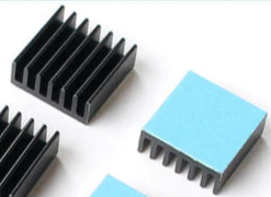
These 14mm ones are common, and 20mm ones may fit too ?
@TonyB_ said:
3. Same voltage regulators as latest EDGE with 5V-16V supply
That's larger, and the one used specs : Wide Input Voltage Range:3.6V to 20V so I'm not sure what the gain is there ?
@knivd said:
Update:
After a few months delay, the first prototypes are a fact, and a good one too.
I am currently designing a board for one of my current projects and will have a chance to test the Stamp in it in real life conditions soon, after which if the results are good, will start thinking how to make it available to a broader market. What puts me off is the terrifying logistics process associated with such activities. Any ideas about that?
Very beautiful! What clocks does it hit reliably? Are they for sale yet?
Not yet. I am just about to complete a PCB which uses this module in a practical application, and will report the achieved performance then.
In any case, I do not have the resource nor the time to handle manufacturing, sales and logistics, so it is unlikely I will do this myself. If someone else is interested in taking over to make this reach the market, I will happily supply the sources and whatever other help I can. This is a serious invitation


Comments
In the schematic, Q1 and Q2 look reversed. The Drains (terminal 3) aren't normally put on the supply side. The forward biased ESD diode stood out to me.
EDIT: Never mind, I see they latch on after the diodes conduct. I presume that is some kind of soft-start circuit?
EDIT2: Reading the datasheet, those transistors are good for 5 amps each continuous. Why use two?
Those are well known way for reverse input protection. Here is one of the possible references (see fig.5):
https://www.maximintegrated.com/en/design/technical-documents/app-notes/6/636.html
Ah, removes the diode drop that would come with a regular diode protection. Still, two of them seems way overkill.
PS: Seriously high amount of scripting for no decent reason in that webpage.
Thanks for posting your schematic @knivd . Yes I recognized the reverse voltage protection with that input FET pair. A while back I noticed you had mentioned you could take up to 20V input:
But the CSD25485F5 FETs seem to list Vgs as -12V max. So be careful with your input voltage when you test. To widen the input voltage range a zener diode can be used between the gate and source to clamp it, with a resistor from gate to ground as shown here:
https://components101.com/articles/design-guide-pmos-mosfet-for-reverse-voltage-polarity-protection
If you do find you need a board rev maybe some of this can be added if there is any room (you could share the one circuit over both FET gates). It'd be nice to accept up to 15V or so for automotive type applications and your -20V Vds rated PFET and LTM4622 would allow that voltage and reverse protect it without frying, except for the gate voltage issue.
With that HyperRAM right there, care to hook a pin to a TV and run one of my emulators? (If you configure to direct boot a ROM, you don't really need input). So far I think the record for any non-Parallax board is running for like 10 minutes before crashing.
If it keeps going over night, you've got a true winner on your hands.
I noted that is built-in to the CSD25485F5. So knivd has that covered to.
Curious that the datasheet has Vgs rating at -12V despite that unusual schematic. If we believe the headline numbers, then 12V would be the maximum reverse voltage protection. (Without an external res/dio bleed as suggested).
Ah, I think I see. The protection isn't for Gate input voltage, it's to neuter capacitively coupled drain-gate reverse spikes coming out of the gate back-feeding a gate driver. A Vgs protection as well. Very important for switching/modulating an output load on the drain. EDIT: Grr, no, that's not it completely either. Those are usually zenor (TVS) diodes.
Roger is right, a 20 volt supply will lift Vgs too high.
EDIT2: Just realised Roger's link is using zenors too. And relies on the resistor being of much higher resistance than what would be used in a modulating circuit. I certainly wouldn't use the 100 ohms example. Way too low resistance. Gate capacitance is only 0.5 nF.
I think it would also be the maximum input voltage too, not just the reverse limit. When the PFET is turned on, Vgs is also reaching up to -12V if the input is fed by 12V (since the gate is grounded) as there is barely any drop from drain to source. You probably couldn't safely rate the input to 12V with this design without that zener, it's too close to the limit. 5-9V is fine though to begin with, but given the regulator can reach 20V it'd be rather nice to allow something like a 15-20V range (and reverse protect it too).
Ah, yes indeed. Initially there were different transistors there, which I later changed for some reason (price or availability). I have overlooked that detail, but fortunately it should be easy enough to fix it with your suggested solution. I will modify the schematic for the next revision. Until then, up to 12V input, unfortunately")
Happy to do that. Please send further instructions what is needed, and a suggested schematic for connecting. And what to run, of course
Sounds good. When I took a look at your layout it seemed like you'd have a little bit of wiggle room to stack the nearby resistors for free space and you can get Zener diodes in the 0603 size (or just put them underneath the board). For the tiny incremental part cost of a diode+resistor it'd be well worth the improved input voltage range in a following revision.
If you still ultimately plan to make this available I am certainly interested in some of these, and also powering them at 12V with some margin for supply range safety. Looking forward to seeing how well your board turns out and how fast it can be reliably clocked.
p.s. what's the total thickness of this design with top + bottom components fitted? Something ~5mm? I'm looking for low profile. The original P2 Edge board is 5.5mm which could possibly suit. But its bulky connector is a killer.
The tallest component on the top side is the SD connector - 2.65mm, and on the bottom are only capacitors - 0.5mm. The PCB itself is 1.2mm, so yes - less than 5mm in total, which with an inverted footprint and cutout for the top side (google up and see my ELLO LC1 as a practical realisation of the idea), could give you a pretty thin solution
I like the design. How is the analog performance? (ADC/DAC) Would it make any difference if there were additional linear stages in the power supply?
One of the things to be determined with practical use
Yes. The RevA Eval Board had selectable VIO source between LDOs and a relatively powerful switchmode. That switchmode was very noisy.
I have had very positive previous experience with PSUs from Analog Devices. Reasonably confident that LTM4622 will not disappoint
As mentioned, the simplest possible connection to see what's going on is connecting any single pin directly to an RCA connector for composite video. No external components needed, for the P2 smartpins are indeed smart. (same for VGA/YPbPr/HDMI, but they need a particular order/alignment of pins) Same story for audio, though ideally that'd have series capacitors (Parallax uses 22µF). Still the same for USB, but Parallax uses an overcurrent protection device (and the code is set up to enable it, so the "basepin" given is actually 2 down from the actual D-/D+ pair). (See the Parallax accessory board schematics)
As said, USB is optional (for just seeing if it works. of course it's very unfun without controls) if you use the DIRECT_BOOT config setting to bypass the menu screen.
Code lives here for NeoGeo: https://github.com/IRQsome/NeoYume
And here for Megadrive: https://github.com/IRQsome/MegaYume
MegaYume is easier to set up because it doesn't need a BIOS file and there's loads of freeware ROMs (some linked in readme). Isn't quite as impressive as NeoYume though. The documentation in either repository is hopefully enough to get going. If not, please complain loudly.
I guess the video mode configuration is a bit confusing - for the aforementioned single pin composite video it would be
The other tricky thing is the memory timing calibration, but that's just the nature of the beast. Play with
HYPER_DELAY,HYPER_SYNC_CLOCKandHYPER_SYNC_DATAuntil it works. DELAY probably needs to be lowered with such a tightly packed design.It's gonna be the first to be reliable at sysclock/1.
Oh my, I don't even have support for that. But indeed, fast brr it may go. But only 16 MB ;/
In reverse direction, the drain is negative and there is no bias on the gate.
In forward direction, many parts these days show an included ESD Zener diode, so an external zener may not be needed, just a series gate resistor.
A device could be tested with a 100k series gate R, to see what clamp actually occurs.
PFETS get smarter these days, I see this for a Diodes DMP2043UCA3 - that has 2 R and Zener internally - they rate the gate at 20v
Series Gate Resistance Rg ~20 < 30 Ω
Series Clamp Resistance RC ~14000 Ω
The 14k series R will give a softer start, tho in reverse use, the D-S clamp diode means it will be 'fast' to ~4.3v and then slower from 4v3 to 5v
I wonder if there is a 'better order' for Q1 and Z1 ? Normal on board use would ramp 5v slowly, but external bench supply of 5V connected live, could generate spikes in that L-R-L-C-L-C ?
I think there is a need for entry-level P2 hardware that is easy to use and a 84-pin PLCC module could perform that function very well. I suggest making it as simple and low-cost as possible to maximize the appeal of the product, as follows:
Well, with the exception of (1) and (3), everything else is easy achievable by just not fitting those components on board. I am not completely sure why (1) would be a problem to anyone, given the fact that the module fits into a socket.
I'd Tony's version but with the flash (16M like Edge).
(1) mainly for heat dissipation if module soldered to motherboard. Also room for caps on top if other stuff not there.
Jon, at the very least that would be a good option.
bottom side decoupling will work better, as the total decoupling pathways can be smaller.
The motherboard just needs to be routed to allow for the caps, tho maybe they could be shuffled a little to manage simpler slot routing on any motherboard.
The most common usage by far would be in a socket, and that has poor thermal paths, so top side heatsink fins seems the best way to add more cooling, if users really need that.
These 14mm ones are common, and 20mm ones may fit too ?
That's larger, and the one used specs : Wide Input Voltage Range:3.6V to 20V so I'm not sure what the gain is there ?
@jmg
I am just about to receive those very heatsinks for my Edge modules. Only (currently) running @180MHz so no real need but I like the look of them
Craig
Very beautiful! What clocks does it hit reliably? Are they for sale yet?
Not yet. I am just about to complete a PCB which uses this module in a practical application, and will report the achieved performance then.
In any case, I do not have the resource nor the time to handle manufacturing, sales and logistics, so it is unlikely I will do this myself. If someone else is interested in taking over to make this reach the market, I will happily supply the sources and whatever other help I can. This is a serious invitation