Just messed with SMPS smartpin mode and got something experimentally working to light the activity LED (P38) in sympathy with the SD CS signal on another pin (P35) going low and turning off when high. Another small bonus is that its brightness when lit (or off) can also be controlled via a PWM value.
Your choice of MOSFET has a questionable gate cutoff voltage and Rds(on). A NTJD4152P will fit in the same footprint, but turns on at a significantly lower gate voltage, which should guarantee <250mOhm at 3.3v drive, while the UM6J1NTN only describes Rds(on) at 4v drive (with .75v potential offset) at 1.2ohms.
Some inconsistent behavior may be fixed by changing it.
Yeah @Circuitsoft it's not necessarily the ideal part for the job and I wouldn't want to choose it for any production. I did notice the Rds was a little high as well at the time and the curve was not shown for -3.3Vgs, but for the smallish SD current draw and reservoir cap fitted on the output it might help form an RC filter for the SD supply to remove noise. Also the doubling up should actually help halve the Rds resistance. Certainly if I do see strange behavior I can try to replace it.
EDIT: I should just throw a set 150mA current load on the SD power pin and see what drop I get across the pFET pair...
EDIT2: Did just that. Voltage dropped from 3.32 to 3.13 with 22ohms put directly across the main capacitor (142mA load + few mA of power LED current). So not too bad under load and similar to some 5% power supply tolerance effect. It acts like a 1.3 ohm resistor at this current.
EDIT3: Actually the above was with the SD card fitted too. When I removed the card and re-applied the 22ohm load resistor, the voltage only fell to 3.15V so it's more like 1.2 ohms at that load.
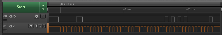
Had a quick play around tonight with the SD card's CMD signal and some SPIN2 test code and hit the first snag.
I'm trying to generate a 48 bit command on the SD CMD pin using the sync tx smart pin mode and the SD CLK pin as the clock source, driven in a smart pin pulse mode by the P2 to control the clock cycles. I setup the sync tx to generate 24 bit data which I send twice to form the 48 bits. But I'm seeing the output clock lag by one data bit which is weird. The clock is started manually in pulse mode so I can send 24 clocks at a time.
I want the clock to be idling high (active low) so the pullups can keep it under control if/when it's released, in reset etc. The pulse output mode normally idles low so I've inverted its output. I've also inverted the clock source input for the sync tx smart pin so the data bits change on the falling edge of the clock input.
In my capture the data bits are changing on the falling edge of this clock which is good, but the problem is that everything looks to be off by one bit below. How can the data be getting generated before the clock pin actually transitions low and is detected by the sync tx smart pin? It's weird. Must be doing something wrong.
Here's the sample test code and what I'm seeing on the two P2 IO pins (CMD and CLK).
CON
BAUD = 115200
SD_CMD = 4
SD_CLK = 5
OBJ
f:"ers_fmt"
uart:"SmartSerial"
PUB main() | x
uart.start(BAUD)
send:=@uart.tx
send("Press a key to start SD test...")
send(uart.rx(),13,10)
send("Initializing pins",13,10)
initpins()
send("Sending command",13,10)
sendcmd(3, $55)
send("Done",13,10)
repeat
PUB initpins()
' setup the clock pin
pinf(SD_CLK)
wrpin(SD_CLK, P_INVERT_OUTPUT | P_OE | P_PULSE) ' want active low clock, idling high
wxpin(SD_CLK, 500<<16 | 1000) ' 50% duty cycle, divide clock by 1000 for testing with logic analyzer
pinh(SD_CLK) ' enable the clock smart pin
akpin(SD_CLK)
PUB sendcmd(cmd, arg) | crc7, a, b
' todo: compute crc7
crc7 := 0
send("cmd=",f.hex(cmd), ", arg=", f.hex(arg),13,10)
send("cmd|arg|crc = ",f.hexn(cmd, 2),f.hexn(arg,8),f.hexn((crc7<<1)|1, 2),13,10)
a := (cmd << 24 | arg >> 8) rev 31
b := (((arg & $ffff) << 16) | (crc7 << 9) | $100) rev 31
send("a=",f.hexn(a,6), ", b=", f.hexn(b,6),13,10)
pinf(SD_CMD) ' reset smart pin
wrpin(SD_CMD, P_INVERT_B | P_PLUS1_B | P_OE | P_SYNC_TX) ' sync tx mode, clk is pin+1 inverted
wxpin(SD_CMD, %1_10111) ' will tx 24 bits twice
wypin(SD_CMD, a) ' prepare first 24 bits
pinh(SD_CMD)
wypin(SD_CLK, 24)' send first 24 bit clocks
' send("1",13,10)
repeat until pinread(SD_CLK) ' wait until all clocks are sent
akpin(SD_CLK)
wypin(SD_CMD, b) ' setup next 24 bits
wypin(SD_CLK, 24) ' send second 24 bit clocks
' send("2",13,10)
repeat until pinread(SD_CLK)
' send("3",13,10)
pinf(SD_CMD) ' reset smart pin once done
akpin(SD_CLK)
You'll be getting some excess old bits left in the shifter. I had a horrible time trying to get consistency from the tx smartpin's "start-stop" mode. I found "continuous" mode far better to run smoothly. But continuous mode does, of course, requires a little more management with the DIR low/high start sequencing.
Here's an example working SPI snippet from sdmm.cc:
// Smartpin SPI transmitter using "continuous" mode and 32-bit word size
// NOTE: data out always has at least a 4 sysclock lag
__asm const { // "const" prevents use of FCACHE
dirl PIN_DI // reset tx smartpin, clears excess data
setq #1
rdlong bc2, buff // fetch first data
rev bc2
movbyts bc2, #0x1b // endian swap
wypin bc2, PIN_DI // first data to tx shifter
mov bc2, bc
shr bc, #2 wz // longword count (rounded down)
shl bc2, #3 // bit count (exact)
wypin bc2, PIN_CLK // begin SPI clocks
dirh PIN_DI // liven tx buffer, continuous mode
add buff, #8
rev d
movbyts d, #0x1b // endian swap
tx_loop
if_nz wypin d, PIN_DI // data to tx buffer
if_nz rdlong d, buff // fetch next data
if_nz add buff, #4
if_nz rev d
if_nz movbyts d, #0x1b // endian swap
tx_wait
if_nz testp PIN_DI wc // wait for tx buffer empty
if_nc_and_nz jmp #tx_wait
if_nz djnz bc, #tx_loop
// Wait for completion
tx_wait2
testp PIN_CLK wc
if_nc jmp #tx_wait2
dirl PIN_DI // reset tx smartpin to clear excess data
wypin ##-1, PIN_DI // TX 0xFF, continuous mode
dirh PIN_DI
PS: Variable "d" is located immediately after "bc2" in cogRAM. The SETQ/RDLONG fills both with the first 64 bits of data. It was a late change and I never commented on it in the source code.
Yes, I think what might be happening is that the LSB data bit0 is already in the shifter and when the first clock happens then bit1 is clocked out. I can probably fix this by shifting the 24 bits up one bit before writing the data with WYPIN...
I've set it up for transmitting 25 bits in each half of the 48 bits. I shift the first data half by a bit but I don't need to shift the second half. I've put one bits in the start and end of each half and it seems to be doing the right thing.
With receive on the CMD pin it'd be nice to be able to use async RX mode given that the response from the SD card starts with a zero bit. But we need to receive more than 32 bits. I wonder if there's some way to start out in async mode and then somehow switch on the fly into sync mode at some given boundary. Maybe by stopping the clock after the first bit arrives or something. I was also wondering if my LED pin could be used as a receiver helper by running it as another smartpin in sync rx mode somehow triggered after the async rx smartpin interrupts to get the remaining data....? The LED can still potentially be controlled by its OUT pin.
Yeah, I've not looked at SD rx timings at all yet. I fear using the streamer will result in needing a working buffer to extract the valid data from. On the other hand, if CRC is to be validated then such a working buffer will be needed anyway.
Ie: I've not seen anything that states a particular number of clocks from command to response nor to rx data block start. It seems to be whatever the SD card feels like within the timeout limit. Up to 100 ms.
Yeah the streamer might not be a go for DAT pins. Because sector data appears to be sent MSB first, which doesn't make a lot of sense to me. I think what might make sense is to read nibbles synchronously and assemble bytes, compute CRCs and write to LUTRAM backwards, then write to HUB using setq2. But I need to look into that more.
EDIT: CRCs seem to be done independently on each bit lane too!
EDIT2: might be able to do 32 bits at a time on each bit lane and munge from there (with clock gaps perhaps)
Big-endian nibble order is handled by streamer no problem. I think the streamer is still the solution. Just it'll need two working buffers to hold maybe 700 bytes each - Provides a decent preamble space for delayed blocks. Not sure how much variability there will be.
Hoping to process the previous read buffer while reading the next one. Probably won't be able to go as fast because of the processing but still should be relatively efficient.
@evanh said:
Big-endian nibble order is handled by streamer no problem. I think the streamer is still the solution. Just it'll need two working buffers to hold maybe 700 bytes each - Provides a decent preamble space for delayed blocks. Not sure how much variability there will be.
It'd be great to use the streamer. But looking at some docs I think the highest bytes in the 512 byte sector appear to be transferred first (so it's not just the nibble order). Surely I have this wrong. All DMA stuff would get broken that way unless it reads memory backwards.
Hoping to process the previous read buffer while reading the next one. Probably won't be able to go as fast because of the processing but still should be relatively efficient.
Yeah we can probably gap the clock temporarily if required. Certainly not a problem for the CMD line performance in doing so, though commands will need extra clocks at the end to be able to completely transmit their response.
@Wuerfel_21 said:
You only actually need to compute CRC for commands and write data. Checking the read CRC isn't enforced.
Yeah. CMD CRC on the 48 bits is pretty easy to do as you can do it before you begin transmission and it covers so few bits, it'll take very little time really in PASM. The data CRCs written get tricky because there are 4 of them if 4 DAT lines are used. Maybe we can stream and compute CRCs in parallel by reading into LUT and serializing...
If the streamer is used we could compute the 4 DAT lane CRCs in parallel from a LUT RAM buffer. This takes ~ 2800 clocks per sector, so you could process ~100k sectors per second at 280MHz which is in the vicinity of 50MBps, and over 25MBps @ 50MHz SD clock. ie. it runs faster than the streamer needs to be clocking out its nibbles.
setq2 #128-1 ' 512 bytes
rdlong 0, databuf ' read from HUB to LUT
rep #10, #128 ' repeat 128 times (@21 clocks per iteration = 2688 cycles)
rdlut data, ptra++ ' get data
setq data
crcnib crc3, poly
crcnib crc3, poly
crcnib crc2, poly
crcnib crc2, poly
crcnib crc1, poly
crcnib crc1, poly
crcnib crc0, poly
crcnib crc0, poly
@evanh said:
Cool! So that could be rdlut inb, ptra++
BTW: That first RDLUT should be a RDLONG instead.
Yeah, noticed my typo and fixed it above.
I think the DAT thing must be sent lowest byte of the sector first (but high nibble). If that's true we could use the streamer for writes, and hopefully reads also once we somehow detect the start bit. We don't have to check the read sector's CRC if we don't want to worry about possible corruption.
Ah, the data order is just written as big-endian because SD is just following SPI convention. What data goes first is still a matter of interpretation. Big-endian says the first word is the most significant, but little-endian says the first word is least significant. That doesn't necessarily mean the data actually changes. The data can be the same order. IBM did a slightly weird trick just like this for its POWER ISA endianess. The labelling of significance swapped but the instruction encoding order actually stayed the same. At least on paper.
And really, that's exactly how a byte addressed true big-endian system works too. The lowest addressed byte goes first. That just happens to be deemed most significant.
EDIT: It comes down to smallest address unit, which is usually the byte. Probably the only question is whether the first nibble is high order or low order of the first byte. My guess is it follows SPI again and the first nibble is the high order bits.
Here's one from Ariba I found somewhere on the forum. It was likely wrapped in Spin2 code originally. I don't even remember if it was for SD cards or not. I think it was:


Comments
Hmm, yeah, that's about the only smartpin mode that does both input and output combined. And it was a late addition at that. JMG requested it I think.
Just messed with SMPS smartpin mode and got something experimentally working to light the activity LED (P38) in sympathy with the SD CS signal on another pin (P35) going low and turning off when high. Another small bonus is that its brightness when lit (or off) can also be controlled via a PWM value.
This combination seemed to work:
_dirl(38); // pin 38 = LED (active low), 35 = !SD_CS _wrpin(38, 0x0d000054); // A=pin B=inv(38-3=35), SMPS mode _wxpin(38, 0x01000010); // base = $10, period = $100 _wypin(38, 0x100); // PWM level _drvl(38); // enable smartpin while(1) { _pinl(35); printf("%8x\n", inb); _waitMs(500); _pinh(35); printf("%8x\n", inb); _waitMs(500); }Your choice of MOSFET has a questionable gate cutoff voltage and Rds(on). A NTJD4152P will fit in the same footprint, but turns on at a significantly lower gate voltage, which should guarantee <250mOhm at 3.3v drive, while the UM6J1NTN only describes Rds(on) at 4v drive (with .75v potential offset) at 1.2ohms.
Some inconsistent behavior may be fixed by changing it.
Yeah @Circuitsoft it's not necessarily the ideal part for the job and I wouldn't want to choose it for any production. I did notice the Rds was a little high as well at the time and the curve was not shown for -3.3Vgs, but for the smallish SD current draw and reservoir cap fitted on the output it might help form an RC filter for the SD supply to remove noise. Also the doubling up should actually help halve the Rds resistance. Certainly if I do see strange behavior I can try to replace it.
EDIT: I should just throw a set 150mA current load on the SD power pin and see what drop I get across the pFET pair...
EDIT2: Did just that. Voltage dropped from 3.32 to 3.13 with 22ohms put directly across the main capacitor (142mA load + few mA of power LED current). So not too bad under load and similar to some 5% power supply tolerance effect. It acts like a 1.3 ohm resistor at this current.
EDIT3: Actually the above was with the SD card fitted too. When I removed the card and re-applied the 22ohm load resistor, the voltage only fell to 3.15V so it's more like 1.2 ohms at that load.
Had a quick play around tonight with the SD card's CMD signal and some SPIN2 test code and hit the first snag.
I'm trying to generate a 48 bit command on the SD CMD pin using the sync tx smart pin mode and the SD CLK pin as the clock source, driven in a smart pin pulse mode by the P2 to control the clock cycles. I setup the sync tx to generate 24 bit data which I send twice to form the 48 bits. But I'm seeing the output clock lag by one data bit which is weird. The clock is started manually in pulse mode so I can send 24 clocks at a time.
I want the clock to be idling high (active low) so the pullups can keep it under control if/when it's released, in reset etc. The pulse output mode normally idles low so I've inverted its output. I've also inverted the clock source input for the sync tx smart pin so the data bits change on the falling edge of the clock input.
In my capture the data bits are changing on the falling edge of this clock which is good, but the problem is that everything looks to be off by one bit below. How can the data be getting generated before the clock pin actually transitions low and is detected by the sync tx smart pin? It's weird. Must be doing something wrong.
Here's the sample test code and what I'm seeing on the two P2 IO pins (CMD and CLK).
CON BAUD = 115200 SD_CMD = 4 SD_CLK = 5 OBJ f:"ers_fmt" uart:"SmartSerial" PUB main() | x uart.start(BAUD) send:=@uart.tx send("Press a key to start SD test...") send(uart.rx(),13,10) send("Initializing pins",13,10) initpins() send("Sending command",13,10) sendcmd(3, $55) send("Done",13,10) repeat PUB initpins() ' setup the clock pin pinf(SD_CLK) wrpin(SD_CLK, P_INVERT_OUTPUT | P_OE | P_PULSE) ' want active low clock, idling high wxpin(SD_CLK, 500<<16 | 1000) ' 50% duty cycle, divide clock by 1000 for testing with logic analyzer pinh(SD_CLK) ' enable the clock smart pin akpin(SD_CLK) PUB sendcmd(cmd, arg) | crc7, a, b ' todo: compute crc7 crc7 := 0 send("cmd=",f.hex(cmd), ", arg=", f.hex(arg),13,10) send("cmd|arg|crc = ",f.hexn(cmd, 2),f.hexn(arg,8),f.hexn((crc7<<1)|1, 2),13,10) a := (cmd << 24 | arg >> 8) rev 31 b := (((arg & $ffff) << 16) | (crc7 << 9) | $100) rev 31 send("a=",f.hexn(a,6), ", b=", f.hexn(b,6),13,10) pinf(SD_CMD) ' reset smart pin wrpin(SD_CMD, P_INVERT_B | P_PLUS1_B | P_OE | P_SYNC_TX) ' sync tx mode, clk is pin+1 inverted wxpin(SD_CMD, %1_10111) ' will tx 24 bits twice wypin(SD_CMD, a) ' prepare first 24 bits pinh(SD_CMD) wypin(SD_CLK, 24)' send first 24 bit clocks ' send("1",13,10) repeat until pinread(SD_CLK) ' wait until all clocks are sent akpin(SD_CLK) wypin(SD_CMD, b) ' setup next 24 bits wypin(SD_CLK, 24) ' send second 24 bit clocks ' send("2",13,10) repeat until pinread(SD_CLK) ' send("3",13,10) pinf(SD_CMD) ' reset smart pin once done akpin(SD_CLK)You'll be getting some excess old bits left in the shifter. I had a horrible time trying to get consistency from the tx smartpin's "start-stop" mode. I found "continuous" mode far better to run smoothly. But continuous mode does, of course, requires a little more management with the DIR low/high start sequencing.
Here's an example working SPI snippet from sdmm.cc:
// Smartpin SPI transmitter using "continuous" mode and 32-bit word size
//   NOTE: data out always has at least a 4 sysclock lag
    __asm const {       // "const" prevents use of FCACHE
        dirl    PIN_DI      // reset tx smartpin, clears excess data
        setq    #1
        rdlong  bc2, buff   // fetch first data
        rev bc2
        movbyts bc2, #0x1b  // endian swap
        wypin   bc2, PIN_DI // first data to tx shifter

        mov bc2, bc
        shr bc, #2  wz  // longword count (rounded down)
        shl bc2, #3     // bit count (exact)
        wypin   bc2, PIN_CLK    // begin SPI clocks

        dirh    PIN_DI      // liven tx buffer, continuous mode
        add buff, #8
        rev d
        movbyts d, #0x1b    // endian swap
tx_loop
    if_nz   wypin   d, PIN_DI   // data to tx buffer
    if_nz   rdlong  d, buff     // fetch next data
    if_nz   add buff, #4
    if_nz   rev d
    if_nz   movbyts d, #0x1b    // endian swap
tx_wait
    if_nz   testp   PIN_DI  wc  // wait for tx buffer empty
if_nc_and_nz    jmp #tx_wait
    if_nz   djnz    bc, #tx_loop

// Wait for completion
tx_wait2
        testp   PIN_CLK  wc
    if_nc   jmp #tx_wait2

        dirl    PIN_DI      // reset tx smartpin to clear excess data
        wypin   ##-1, PIN_DI    // TX 0xFF, continuous mode
        dirh    PIN_DI
PS: Variable "d" is located immediately after "bc2" in cogRAM. The SETQ/RDLONG fills both with the first 64 bits of data. It was a late change and I never commented on it in the source code.
Yes, I think what might be happening is that the LSB data bit0 is already in the shifter and when the first clock happens then bit1 is clocked out. I can probably fix this by shifting the 24 bits up one bit before writing the data with WYPIN...
Oh, you're actually using start-stop wrongly. You're meant to make DIR high before WYPIN. What you've done would suit continuous mode.
Well it's ugly but it works.
I've set it up for transmitting 25 bits in each half of the 48 bits. I shift the first data half by a bit but I don't need to shift the second half. I've put one bits in the start and end of each half and it seems to be doing the right thing.
Yeah I think I got that control bit the wrong way around. I'll have to try the other option out.
With receive on the CMD pin it'd be nice to be able to use async RX mode given that the response from the SD card starts with a zero bit. But we need to receive more than 32 bits. I wonder if there's some way to start out in async mode and then somehow switch on the fly into sync mode at some given boundary. Maybe by stopping the clock after the first bit arrives or something. I was also wondering if my LED pin could be used as a receiver helper by running it as another smartpin in sync rx mode somehow triggered after the async rx smartpin interrupts to get the remaining data....? The LED can still potentially be controlled by its OUT pin.
Yeah, I've not looked at SD rx timings at all yet. I fear using the streamer will result in needing a working buffer to extract the valid data from. On the other hand, if CRC is to be validated then such a working buffer will be needed anyway.
Ie: I've not seen anything that states a particular number of clocks from command to response nor to rx data block start. It seems to be whatever the SD card feels like within the timeout limit. Up to 100 ms.
Yeah the streamer might not be a go for DAT pins. Because sector data appears to be sent MSB first, which doesn't make a lot of sense to me. I think what might make sense is to read nibbles synchronously and assemble bytes, compute CRCs and write to LUTRAM backwards, then write to HUB using setq2. But I need to look into that more.
EDIT: CRCs seem to be done independently on each bit lane too!
EDIT2: might be able to do 32 bits at a time on each bit lane and munge from there (with clock gaps perhaps)
Big-endian nibble order is handled by streamer no problem. I think the streamer is still the solution. Just it'll need two working buffers to hold maybe 700 bytes each - Provides a decent preamble space for delayed blocks. Not sure how much variability there will be.
Hoping to process the previous read buffer while reading the next one. Probably won't be able to go as fast because of the processing but still should be relatively efficient.
You're right about the CRC though, it'll process much easier coming from serial smartpins pre-merging of data.
You only actually need to compute CRC for commands and write data. Checking the read CRC isn't enforced.
It'd be great to use the streamer. But looking at some docs I think the highest bytes in the 512 byte sector appear to be transferred first (so it's not just the nibble order). Surely I have this wrong. All DMA stuff would get broken that way unless it reads memory backwards.
Yeah we can probably gap the clock temporarily if required. Certainly not a problem for the CMD line performance in doing so, though commands will need extra clocks at the end to be able to completely transmit their response.
Yeah. CMD CRC on the 48 bits is pretty easy to do as you can do it before you begin transmission and it covers so few bits, it'll take very little time really in PASM. The data CRCs written get tricky because there are 4 of them if 4 DAT lines are used. Maybe we can stream and compute CRCs in parallel by reading into LUT and serializing...
If the streamer is used we could compute the 4 DAT lane CRCs in parallel from a LUT RAM buffer. This takes ~ 2800 clocks per sector, so you could process ~100k sectors per second at 280MHz which is in the vicinity of 50MBps, and over 25MBps @ 50MHz SD clock. ie. it runs faster than the streamer needs to be clocking out its nibbles.
setq2 #128-1 ' 512 bytes rdlong 0, databuf ' read from HUB to LUT rep #10, #128 ' repeat 128 times (@21 clocks per iteration = 2688 cycles) rdlut data, ptra++ ' get data setq data crcnib crc3, poly crcnib crc3, poly crcnib crc2, poly crcnib crc2, poly crcnib crc1, poly crcnib crc1, poly crcnib crc0, poly crcnib crc0, polyYou can leave off the SETQ, RDLUT already sets Q for you.
LOL, Yeah I thought it might but your docs under RDLUT didn't show that when I just looked. I should have looked up the Q register instead.
Yeah, RDLUT is just a stub rn.
Cool! So that could be
rdlut inb, ptra++BTW: That first RDLUT should be a RDLONG instead.
Yeah, noticed my typo and fixed it above.
I think the DAT thing must be sent lowest byte of the sector first (but high nibble). If that's true we could use the streamer for writes, and hopefully reads also once we somehow detect the start bit. We don't have to check the read sector's CRC if we don't want to worry about possible corruption.
Ah, the data order is just written as big-endian because SD is just following SPI convention. What data goes first is still a matter of interpretation. Big-endian says the first word is the most significant, but little-endian says the first word is least significant. That doesn't necessarily mean the data actually changes. The data can be the same order. IBM did a slightly weird trick just like this for its POWER ISA endianess. The labelling of significance swapped but the instruction encoding order actually stayed the same. At least on paper.
And really, that's exactly how a byte addressed true big-endian system works too. The lowest addressed byte goes first. That just happens to be deemed most significant.
EDIT: It comes down to smallest address unit, which is usually the byte. Probably the only question is whether the first nibble is high order or low order of the first byte. My guess is it follows SPI again and the first nibble is the high order bits.
Q Register instruction missing from your doc:
Thank you, quality observation. Fixed.
Took some finagling but I think this CRC7 generator is right...
PUB gencrc7(cmd, arg) : crc | poly
asm
    mov poly, #$48      ' CCITT polynomial is x^7 + x^3 + 1 (bit reversed for P2 and aligned on "bit-1")
    mov crc, arg        ' prepare an initial CRC value in its 32 bit long
    shr crc, #8         ' using cmd & arg data
    setbyte crc, cmd, #3' prepare first byte with cmd bits
    rev crc             ' reverse CRC bits because P2 CRC HW shifts right
    shl arg, #24        ' align remaining 8 arg bits
    setq #0             ' setup remaining data for CRC
    rep #1, #8          ' CRC on 40 bits is 10 nibbles
    crcnib crc, poly    ' compute CRC
    setq arg            ' setup remaining data for CRC
    crcnib crc, poly    ' compute CRC
    crcnib crc, poly    ' compute CRC
    rev crc             ' reverse bits
    shr crc, #25        ' keep 7 top bits
endasm
compared with this:
https://github.com/hazelnusse/crc7/blob/master/crc7.cc
Here's one from Ariba I found somewhere on the forum. It was likely wrapped in Spin2 code originally. I don't even remember if it was for SD cards or not. I think it was:
uint32_t  crc7( uint8_t * buf, int len )
{
    uint32_t  val, crc = 0;

    __asm {
// Reference code courtesy of Ariba
cr7lp
        rdbyte  val, buf
        add buf, #1
        shl val, #24
        setq    val
        crcnib  crc, #$90>>1
        crcnib  crc, #$90>>1
        djnz    len, #cr7lp

        rev crc
        shr crc, #24
        or  crc, #1
    }
    return crc;
}
And the CRC16 one:
uint32_t  crc16( uint32_t * buf, int len )
{
    uint32_t  val, crc = 0,
    polynomial = 0x8408;  // CRCNIB shifts right, therefore ordered from left: x0 + x5 + x12

    __asm volatile {    // disable optimising, and enforces Fcache use
// Reference code is courtesy of Ariba
        rdfast  #0, buf
        mov ptra, #0

        rep @.rend, len
        rflong  val
        setq    val
        crcnib  crc, polynomial
        crcnib  crc, polynomial
        crcnib  crc, polynomial
        crcnib  crc, polynomial
        crcnib  crc, polynomial
        crcnib  crc, polynomial
        crcnib  crc, polynomial
        crcnib  crc, polynomial
.rend
        rev crc
        shr crc, #16
    }
    return crc;
}