

New SD mode P2 accessory board
 rogloh
Posts: 6,410
rogloh
Posts: 6,410
I've been meaning to make this for a while but finally the boards arrived today.
This PCB should hopefully allow some experiments with micro SD cards in full SD transfer mode on a P2 accessory board with the P2-EVAL etc.
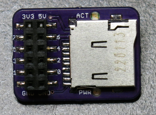
I've got the SDIO and other controls mapped to P2 pins as follows. Whether or not this pin mapping is optimal is still TBD. I expect it should be possible to also use a card in SPI mode as well if the correct P2/SD pins are mapped to the SD driver.
- Pin offset - SD signal
- P0-P3 - DAT0-DAT3
- P4 CMD
- P5 CLK
- P6 ACTIVITY LED
- P7 !CARD DETECT/POWER_DOWN
Power to the SD card can be controlled by a FET for card reset purposes. The board defaults to power on if a card is present, but it can be shutdown if P7 is optionally driven high. Used as an input, P7 will also read high if no card is detected by the hardware, and low if a card is present. The card power state is indicated by a dedicated power LED. A general purpose IO pin P6 can also drive a separate activity LED (active low). The LEDs shine up through holes on the board.
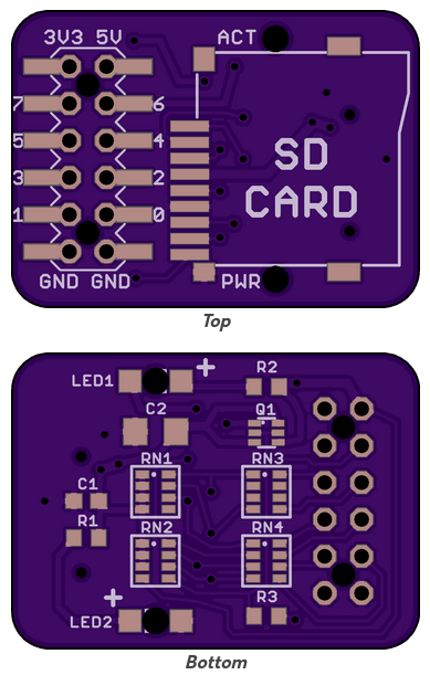
Here are a couple of pictures of the assembled board that I hand soldered this afternoon. It included some nasty 0603 and SOT363 parts but I think I managed to connect it up ok, time will tell. This board is rather small at 20.5x28.5mm. The card reader socket is of the higher quality push-pull latching type with a built in card detect switch that my circuit also uses.
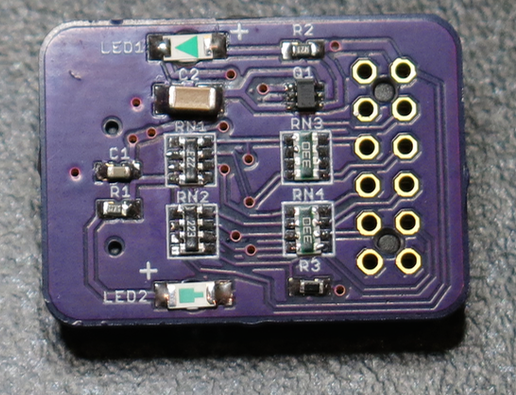
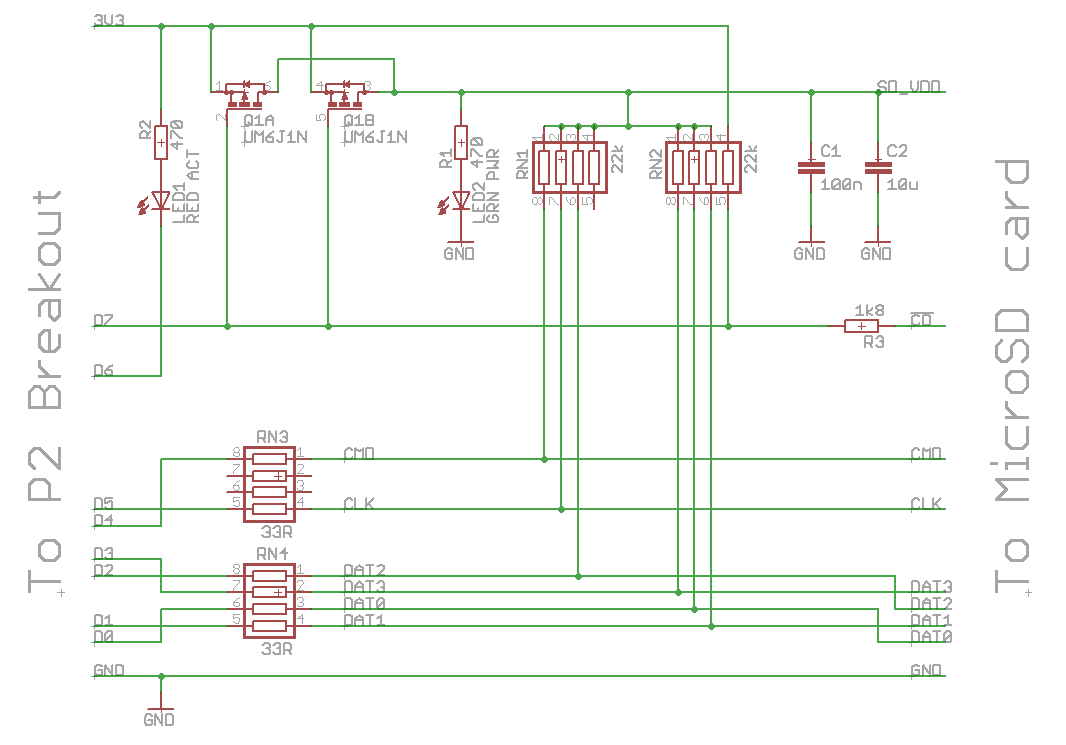
A partial schematic (which I created after the fact, LOL) is also included below as well as the rendered pictures of the PCB layout. I still might have to tweak some component values if the LEDs are too dim/bright or if I get poor data performance. I just picked 33 ohm series resistance and 22k pull ups for now. The PFET choice was just something I had available in my parts bin. It's only a little one so I doubled it up by paralleling both devices in the package and it can carry up to 400mA now (800mA pulse), not that an SD card should need that much current.
I'll probably verify that the basic HW is functional or not in the next few days, but when I have a spare lazy weekend sometime I'll try to see what I can do in SD mode.
Comments
Looks perfect! I want one.")
I could mail you a spare board and the SD socket, maybe a few of the parts if you are handy with an iron. I got 3 boards made and I only need one. Tubular got the other one. PM me if you do want one.
done
Wow that was fast work. It came up looking really nice.
I like what you've done with the leds shining through the holes, there's something very clean about doing it that way
I like that you added power recycling. In my experiences with my 4 sd RAISD board on the P1 I stumbled often over the need to reboot to get the cards working again.
Well done.
Mike
4-bit flexspin VFS driver when?
No promises. Maybe Roger will beat me to it.")
I dunno evanh, recently I have just made about 10 different boards on a range of projects so there is quite a lot going on right now for me on multiple projects. That's why sending one over to you is probably a good idea if you have time to mess around with it as well and get some sectors transferring to the P2.
Thanks Mike and Tubular. The power switching is important if you do SD card mode, yes. I think there is no way to switch back to SPI mode once you enter SD mode without power cycling for example. Yeah the board came out reasonable I think, despite being hand soldered, maybe my hotplate would have given nicer results with SMD part self alignment but I didn't bother making the stencil for this small PCB and just used it for some more soldering practice. Not perfect but it might still work...probably should start messing a little with it tomorrow and at least try out SPI mode.
Roger, could you please tell me the part numbers of those reverse-mount LEDs? I'm searching for some just like that. I've been using LEDs from Osram but unfortunatelly, they have been discontinued. Most I've found so far have very strange dimensions and are either too small or too big. But the one you use have just the right size.
Yeah @ManAtWork, these are their part numbers from Digikey. I ordered some red, green and blue ones to try out, although the red LED diffuser/lens cap thing seemed to be more square shaped than circular compared to the green one and I needed to widen the hole a bit with a drill, so maybe they sent me something else. I've not opened the blue ones yet and they were from a different manufacturer too, Dialight vs Würth Electronik.
732-5030-1-ND red
732-5033-1-ND green
350-2307-1-ND blue
Ahh Those are the Würth style reverse LEDs. I've seen them before. I haven't noticed the "hump" on the PCB side. I thought they were flat. I can't use them because my PCB is only 0.8mm thick and the hump is something >1mm. I have a membrane keyboard on the opposite side so the humps would collide.
Thanks anyway. Currently I'm using those: https://www.mouser.de/ProductDetail/Kingbright/AA3528SYCKT-J309 but they are quite bulky.
? The green LED's data sheet seem to be showing as 1.2mm total height of which 0.4mm is on the solder side, and 0.8mm goes through the PCB. If your PCB is only 0.8mm the LED would sit flush and not interfere with your membrane.
If you need me to double check this for you, I can crack open another green LED and get the calipers out tomorrow once I get up.
Wurth have bi-color versions which have lower profile; about 0.6mm
156125RV73000, 156125RG73000, 156125YV73000
Having trouble getting my new SD board functioning with just the SPI mode and flexspin. All I get is the SD test code hanging during the SD mount sequence.
Obviously thought it was my HW but now I'm not quite so sure...
In frustration I removed my board entirely from the equation and found I am getting different SW results when I reorder pins (that are all now floating) allocated to the SPI bus. So I'm sort of wondering if there is some sort of hidden dependency in the driver with the particular pin allocation that might explain the failure...?
I'm using the latest 5.19.19 flexspin that I downloaded a day or two ago.
Initializing with this pin group works (as in it fails to detect a non-present card - just floating P2 pins)
fs = _vfs_open_sdcardx(41, 43, 42, 40);resulting in:
But initializing with this pin group fails (it hangs forever even though the MISO input readback pin is the same and only CLK and MOSI pins are different. WTH? I also tried the SPI clock as several other pins, 8, 16,17, 46, 47, 48 and got the same.
fs = _vfs_open_sdcardx(45, 43, 44, 40);It hangs here:
The attached SD test code I used is something I found in the forums from earlier this year, and also needed mods to compile with the latest flexspin - some sort of vfs structure change. I can make it work and read a populated card with the default SD card pins.
fs = _vfs_open_sdcardx(61, 60, 59, 58);Results:
All I can assume now is that there is something hidden in the driver SW that somehow depends on the pin order or the CLK being in the same nibble as other signals or somehow within a neighbouring smart pin range? Will play with pin numbers to try to home in a bit more.
Anyone with other ideas?
Where exactly is the P2 source to this SD driver code used by flexspin?
Well whatdya know... look what I found in include/filesys/fatfs/sdmm.cc:
It is a smartpin pin distance issue. There is a dependency on pins being within a certain distance of each other for this code to work. @evanh I think this is your recent stuff, right?
I jumpered SPI CLK directly to DAT2 on my board (it's safe in SPI mode) and ran the code with the CLK moved down in +/- 3 pin smartpin range to MISO and MOSI with this pin setup...
fs = _vfs_open_sdcardx(34, 35, 36, 32);So my board IS working after all! But not directly in SPI mode with the current flexspin SD driver with Evanh's enhancements. It'd probably need the DAT pins in the upper nibble for that to work - or a jumper on the board to enable SPI mode specifically. A respin could do that.
Ouch, of course, that's actually a smartpin hardware limitation. SmartA and SmartB inputs have to be within +-3 pins of the smartpin.
It might still be possible to massage the smartpins to handle the wider arrangement by also redirecting both SmartA and SmartB. By default, SmartA is the same pin as the smartpin ...
EDIT: Err, no that fails for outputs. Only the serial input can be rerouted via SmartA.
EDIT2: But luckily DO, on P40, is the rx data input. Bit of an exception, but still doable ...
fs = _vfs_open_sdcardx(45, 43, 44, 40);Yep!
Maybe. Perhaps this PIN mapping below would have been better to keep CLK within 2 pins away from MISO(DAT0) and MOSI(CMD). Perhaps I didn't agonize over it enough and assumed the P2 driver was not using smart pins. Or I could put a switch/solder jumper on board to select the mode of the board. In theory it's meant to be a SD mode board after all, so supporting SPI is just a bonus really - it just could be handy for a fallback however if the driver can't use SD mode. And I used SPI mode now just to partially test my board out.
Pin offset - SD signal
Oh, yeah I guess a smartpin can be setup on an intermediate pin between the two.
In SPI mode the actual offset between CLK and MOSI is only 1 pin. Perhaps the smartpin for RX can be put onto P2 or P3?
P0 MISO INPUT TO Prop2 (DAT0)
P3 CS (DAT3)
P4 MOSI OUTPUT FROM Prop2 (CMD)
P5 CLK
When you get your board, you might want to try that out.
The pin order looks good for the streamer in 4-bit mode. Shuffling them will mess with that.
EDIT: I don't think the streamer would be happy with the nibble moved up by four bits for example. Maybe it can do this.
EDIT2: But it might be happy with the bits in the opposite order: No, the below wiring won't work. The streamer's order mode bit is for the nibble order in hubRAM, not the pin order.
What you can do right now is drop back to the original flexspin bit-bashed mode. You need to edit that sdmm.cc file and comment out the line with
#define _smartpins_mode_eh /* enable Evanh's fast smartpin code */EDIT: Okay, I've hacked up a replacement sdmm.cc that will use a different smartpin for rx data when the separation of CLK from MISO is larger than three. Throw this over top of your existing sdmm.cc file.
EDIT2: Oops, didn't update the global pin number ... fixed now.
EDIT3: Doh, also used the wrong OR operator in the pin conflict check ... fixed now.
Ok thanks, I'll give it a try tomorrow.
Just tried your fix and it worked! This is a useful change for this board and lets you use more pins further away.
I think now I'll just resolder the other 10k pullup I'd removed for testing and then send you this known working board.
Cool. It uses an unspecified pin's smartpin, so not ideal as a general solution.
In SD mode I think I should be able to have two smartpins handling the command and response on CMD pin and streamer handling the DATx pins. Then there shouldn't be a need for this hack any longer.
On that note, maybe don't need to rearrange the accessory pins either any longer. We have a working comparison to start developing the SD mode from.
I hope to handle overlapping data and command/response at full speed. Ie: Fully implement stop commands.
Yes that would be ideal, as data & commands seem to be partially asynchronous to each other in that mode.
Back to smart pins again in SPI mode. I made sure that the activity LED I put on the board was within 3 pins of the CS pin in SPI mode, so I think it should be possible to setup the output drive of that pin to reflect the logical combination of its own output (master LED enable) and the CS pin state so no special software will have to control this separate LED once the smart pin is initialized. Given it is active low to light the LED then the logic to use is probably just an OR of the CS pin with its own state, although AND could also be used if the master enable input state is treated as inverted and you want to be able to override the LED for other reasons. It's pretty flexible really.
I'll test that out once I make up another board.
Speaking of LEDs I noticed after I changed to 10k pull up resistors that the power LED could be dimly lit when the P2 IO pins are driven even without a card present and this is due to current bleeding into SD power net from the P2 IO pins via the pull ups. I don't think it would be enough current to fully power the SD but you never know, so when the power needs to be switched off for reset purposes in SD mode it would make good sense to also float the P2 IO pins at the same time to make sure that the power net caps fully discharge (which will automatically happen via the LED). To remedy this minor issue in hardware it may make sense to fit a schottky diode between the pullup common and the SD_VDD nets in my schematic to block reverse current, although seeing the LED dimly lit lets you know that the IO pins are actually powered too, so it is potentially somewhat useful as is. Or I could try increasing the pull up resistance to something like 47k...
Might have spoken too soon about the activity LED pin being driven from the CS pin state in SPI mode.
I'd looked at this table:
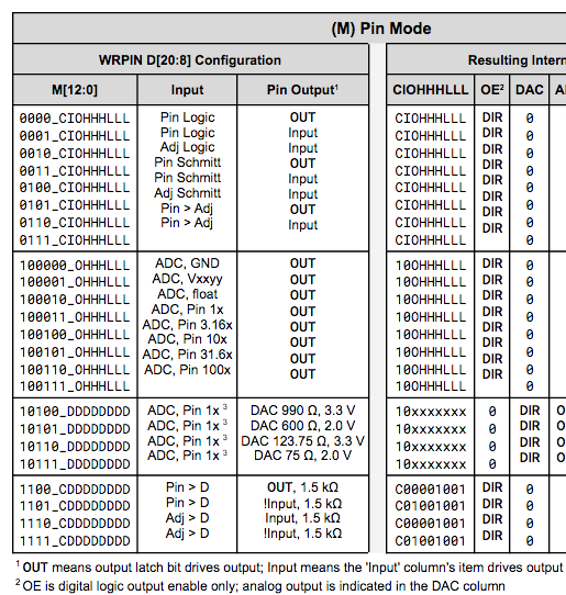
and interpreted the M[12:0] case of 0001_xxxxxxxxx and "Note 1" meaning that the pin output was the same as the input column's state (taken after the logic selector). But when I tried it out the activity LED pin on pin 38 was just high when running this test snippet even though it's own input was seen toggling for that same pin (as well as the CS pin 35 being controlled by the test code).
    _dirl(38); // pin 38 = LED (active low), 35 = !SD_CS
   _wrpin(38, 0x55420000); // A=pin(38-3=35), B=pin, F=OR(A,B)
    _dirh(38);
    while(1)
    {
        _pinl(35);
        _waitMs(500);
        printf("%8x\n", inb);
        _pinh(35);
        _waitMs(500);
        printf("%8x\n", inb);
    }
Output:
I'd done something like this before in the past and was convinced it was possible, but perhaps not. Maybe they were adjacent pins or something or open collector. The documentation above seems a little unclear now.
Chip's A/B naming needs improved. There is two entirely different A and B inputs. There is the low level PinA and PinB which are only an odd/even pair and entirely not the smartpin's A/B input sources. I've been naming the smartpin's A and B inputs SmartA and SmartB.
Okay, having clarified that, SmartA/B inputs cannot be fed back to the pin's output. Whereas PinA/B inputs can be fed back to the pin output.
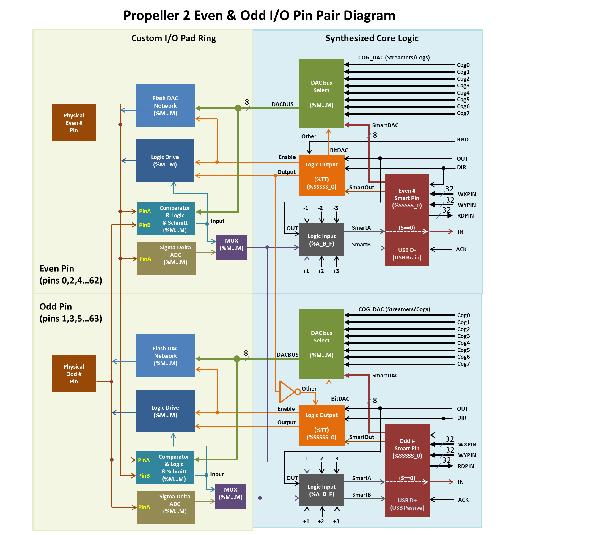
Yeah your diagram is what is missing in the docs @evanh . It's very handy to see the entire structure like this.
I was looking for any smartpin mode that could take its inputs and drive an output based on it. We need something where "SmartOut" depends on SmartA or SmartB above and can be used to drive the output pin. Only thing I found was the PWM SMPS mode with V/I feedback which I now wonder whether could be used somehow. Might look into that one.