This reminds me that wanted to make a large cutout under socket so that could consider soldering module directly onto smt pads where socket is supposed to go...
@Rayman said:
This reminds me that wanted to make a large cutout under socket so that could consider soldering module directly onto smt pads where socket is supposed to go...
Four of the 20way version would suit a much lower cost castellated PCB module. Mind you... 1.27mm pitch headers would also achieve the same at the lowest possible cost (assuming that was a significant aim).
Making a module that supports both castellated and through-hole headers is looking wildly lower cost than making a PLCC compatible PCB at the moment.
Edit: Though if doing a castellated thing, a more compact overall size might be achievable with 1mm pitch castellations and inset TH's suitable for 1mm pitch headers.
@VonSzarvas said:
Making a module that supports both castellated and through-hole headers is looking wildly lower cost than making a PLCC compatible PCB at the moment.
Edit: Though if doing a castellated thing, a more compact overall size might be achievable with 1mm pitch castellations and inset TH's suitable for 1mm pitch headers.
Have you seen the RP2040/2350 stamp modules and FlexyPins solution from SolderParty https://www.solder.party/docs/ ?
I have recently bought the stamp modules and the flexypins seems an interesting solution, although a pain to fit the stamp with all 4 sides.
I think the pitch is 2mm, the wider RP2350 stamp XL seems a good fit for the P2 (not that it must be compatible, just an idea).
Not seen that (thanks; interesting). That's just what I was thinking of. Castellated, 1mm pitch, inset TH. And the module supplied either bare, or with the headers pre-soldered on all 4 sides. Close to what they have done, except we'd be more micro-scale.
@SaucySoliton said:
Wow, only 1 ground pin for 48 gpios. That will be a NOPE for me.
That made me laugh!
Though those castellated/TH pins would probably allow less Pwr/Gnd pins than a PLCC socket. Either way, it seems likely the new module will demand more GND and main VIN pins than Edge.
BTW... We are just exploring various options at the moment- not certain to go one way or the other, and might still end up going the PLCC route. Pricing of the PLCC compatible fingers sure is a motivation to double back and look at other options
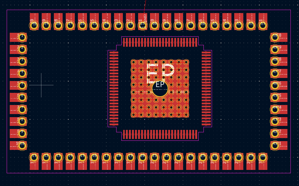
Here's what have for basic board for P2 Stamp. Think need something like this in order to sell the stamp...
SMT version of PLCC socket should allow for Stamp to be directly soldered to PCB without socket, we'll see.
Put in a big hole in the middle to allow that.
Also put in some holes in 3 of the corners that might let one free the module from the socket with a stick of some kind.
That's also TBD...
If Parallax does do a version of Stamp, they'll probably use unleaded solder and have parts on top only.
Means one could put in reflow oven with leaded solder to make connections...
Ordered a thinner stencil. Original is .13 mm. This is too thick for those mosfet friends of mine and think also gives too much for P2 pins and other things.
Hopefully new .1 mm stencil will let some solder down onto the mosfet pads and help with some of these other tiny parts too.
Agreed -- but I have the advantage of lifting good ideas from your design!
If it helps, I'm using the Keystone 1502-2 (Digikey 36-1502-2-ND) turret on my P1 Eval board. The pad is 150mils with a 90mil hole. I didn't spend the $68 on the staking tool, and have found with a bit flux they solder in quite nicely.
@Rayman said:
@VonSzarvas Looks like name "Stamp" is used in other places as @macca pointed out. So, guess the name is free for anybody to use...
My personal opinion is that "Stamp" is long associated with Parallax modules, possibly the first ever uC module, and I wouldn't personally use the name for a product without explicit approval from Ken. And even then, I think I'd steer toward a fresh new naming convention.
To elaborate on my opinion should others less familiar with Parallax be reading this in the future:
I can't speak to what might happen with the naming of this (or any) future new Parallax module, but if it was me I'd want to at least reserve the option to choose the "Stamp" name (or a derivative of) when the process gets to that point. And it might be considered confusing for customers if multiple modules exist with long established Parallax brand/product names.
I've no idea what brand protection Parallax might (or might not) have for the Stamp marque, but regardless I'd personally reach out to Ken via e-mail with an informal approach before investing in the name. We all know how open, fair and supportive Parallax always tries to be, but I think with that it's also important for us to not take advantage or make assumptions that might not be in all parties best interests; especially when it comes to the integrity of the source of the uC's that modules might rely on.
@Rayman said:
If Parallax does do a version of Stamp, they'll probably use unleaded solder and have parts on top only.
Means one could put in reflow oven with leaded solder to make connections...
I'd be sure to use high-temp unleaded solder on the module if it lends itself to customers re-flowing the thing onto their own boards, so the modules can be reliably reflowed with regular LF solder paste.
If we consider that the process adds some cost for all customers, it might be appropriate for the first release to support "manual" soldering only, and have a fully re-flowable module available at a premium with a certain MOQ. Pros and Cons
Edit: Though if doing a castellated thing, a more compact overall size might be achievable with 1mm pitch castellations and inset TH's suitable for 1mm pitch headers.
Speaking only to my use case, this would be the best of the best... Not so BB friendly though...
@Rayman said:
If Parallax does do a version of Stamp, they'll probably use unleaded solder and have parts on top only.
Means one could put in reflow oven with leaded solder to make connections...
I'd be sure to use high-temp unleaded solder on the module if it lends itself to customers re-flowing the thing onto their own boards, so the modules can be reliably reflowed with regular LF solder paste.
If we consider that the process adds some cost for all customers, it might be appropriate for the first release to support "manual" soldering only, and have a fully re-flowable module available at a premium with a certain MOQ. Pros and Cons
That could work.. My current project would have used 60 pcs.. is this in the ballpark MOQ you are talking about?
@"R Baggett" said:
That could work.. My current project would have used 60 pcs.. is this in the ballpark MOQ you are talking about?
I shouldn't say (that would be a Ken thing once the module is launched, and he has the figures). Based on the set-up time and cost, and the need to stock more expensive versions of certain parts, etc.. etc.. (it's a long list)... I could guess that 250 or 500 might be closer to the ballpark. But surely some pooling of customers would be possible.
For me it's handy to see your feedback (thank you), as I constantly consider customer requirements as the design evolves, and it might be we end up targeting more toward high-temp anyway.
My personal opinion is that "Stamp" is long associated with Parallax modules, possibly the first ever uC module, and I wouldn't personally use the name for a product without explicit approval from Ken. And even then, I think I'd steer toward a fresh new naming convention.
That's an interesting point, but seems like there are lots of things called "Stamp" these days:
Guess can see that Parallax might want to reserve the name "Stamp" for their version of this module.
If @"Ken Gracey" doesn't want me to use the name "Stamp", he should let me know right away.
I'm ordering PCBs with the name "Stamp Carrier" on them this weekend...


Comments
This reminds me that wanted to make a large cutout under socket so that could consider soldering module directly onto smt pads where socket is supposed to go...
THAT is exactly how I would use this.
Shame the EDAC castellated module "socket" never seemed to reach mass production pricing.
https://edac.net/products/smt-card-edge-connectors/230
Four of the 20way version would suit a much lower cost castellated PCB module. Mind you... 1.27mm pitch headers would also achieve the same at the lowest possible cost (assuming that was a significant aim).
Making a module that supports both castellated and through-hole headers is looking wildly lower cost than making a PLCC compatible PCB at the moment.
Edit: Though if doing a castellated thing, a more compact overall size might be achievable with 1mm pitch castellations and inset TH's suitable for 1mm pitch headers.
Have you seen the RP2040/2350 stamp modules and FlexyPins solution from SolderParty https://www.solder.party/docs/ ?
I have recently bought the stamp modules and the flexypins seems an interesting solution, although a pain to fit the stamp with all 4 sides.
I think the pitch is 2mm, the wider RP2350 stamp XL seems a good fit for the P2 (not that it must be compatible, just an idea).
Not seen that (thanks; interesting). That's just what I was thinking of. Castellated, 1mm pitch, inset TH. And the module supplied either bare, or with the headers pre-soldered on all 4 sides. Close to what they have done, except we'd be more micro-scale.
It fits!
Wow, only 1 ground pin for 48 gpios. That will be a NOPE for me.
This sounds good to me:
Castellated, 1mm pitch, inset TH. And the module supplied either bare, or with the headers pre-soldered on all 4 sides.
Would definitely reduce cost compared to PLCC.
That made me laugh!
Though those castellated/TH pins would probably allow less Pwr/Gnd pins than a PLCC socket. Either way, it seems likely the new module will demand more GND and main VIN pins than Edge.
So the through hole pins would allow it to plug into a square of female headers right?
Correct. Either plug into lowcost regular pin sockets, or solder down directly.
BTW. Apologies for taking your thread off course a little")
If this way turns out better, might have to copy it…. Think can figure out how to do castellated edges. Not sure can design the stamp edge myself…
Bit concerned about bending the tiny through hole pins, but maybe there will be a hole on host board to help with that.
BTW... We are just exploring various options at the moment- not certain to go one way or the other, and might still end up going the PLCC route. Pricing of the PLCC compatible fingers sure is a motivation to double back and look at other options")
Those LIF pins are great for a bench top, but not in a laser tag "weapon" that players are running around with and frequently dropping.
Here's what have for basic board for P2 Stamp. Think need something like this in order to sell the stamp...
SMT version of PLCC socket should allow for Stamp to be directly soldered to PCB without socket, we'll see.
Put in a big hole in the middle to allow that.
Also put in some holes in 3 of the corners that might let one free the module from the socket with a stick of some kind.
That's also TBD...
If Parallax does do a version of Stamp, they'll probably use unleaded solder and have parts on top only.
Means one could put in reflow oven with leaded solder to make connections...
@VonSzarvas Looks like name "Stamp" is used in other places as @macca pointed out. So, guess the name is free for anybody to use...
Ordered a thinner stencil. Original is .13 mm. This is too thick for those mosfet friends of mine and think also gives too much for P2 pins and other things.
Hopefully new .1 mm stencil will let some solder down onto the mosfet pads and help with some of these other tiny parts too.
If Parallax doesn't do it, I will make a board that matches the size and layout of the P2 Eval. This is just a Diptrace sketch.
@JonnyMac thought about that myself, but looks like too much work for me")
Although guess it’s almost the same thing
Reminds me that want to add those ground holes between headers…
Agreed -- but I have the advantage of lifting good ideas from your design!
If it helps, I'm using the Keystone 1502-2 (Digikey 36-1502-2-ND) turret on my P1 Eval board. The pad is 150mils with a 90mil hole. I didn't spend the $68 on the staking tool, and have found with a bit flux they solder in quite nicely.
This is interesting …
My personal opinion is that "Stamp" is long associated with Parallax modules, possibly the first ever uC module, and I wouldn't personally use the name for a product without explicit approval from Ken. And even then, I think I'd steer toward a fresh new naming convention.
To elaborate on my opinion should others less familiar with Parallax be reading this in the future:
I can't speak to what might happen with the naming of this (or any) future new Parallax module, but if it was me I'd want to at least reserve the option to choose the "Stamp" name (or a derivative of) when the process gets to that point. And it might be considered confusing for customers if multiple modules exist with long established Parallax brand/product names.
I've no idea what brand protection Parallax might (or might not) have for the Stamp marque, but regardless I'd personally reach out to Ken via e-mail with an informal approach before investing in the name. We all know how open, fair and supportive Parallax always tries to be, but I think with that it's also important for us to not take advantage or make assumptions that might not be in all parties best interests; especially when it comes to the integrity of the source of the uC's that modules might rely on.
I'd be sure to use high-temp unleaded solder on the module if it lends itself to customers re-flowing the thing onto their own boards, so the modules can be reliably reflowed with regular LF solder paste.
If we consider that the process adds some cost for all customers, it might be appropriate for the first release to support "manual" soldering only, and have a fully re-flowable module available at a premium with a certain MOQ. Pros and Cons")
>
Speaking only to my use case, this would be the best of the best... Not so BB friendly though...
That could work.. My current project would have used 60 pcs.. is this in the ballpark MOQ you are talking about?
I shouldn't say (that would be a Ken thing once the module is launched, and he has the figures). Based on the set-up time and cost, and the need to stock more expensive versions of certain parts, etc.. etc.. (it's a long list)... I could guess that 250 or 500 might be closer to the ballpark. But surely some pooling of customers would be possible.
For me it's handy to see your feedback (thank you), as I constantly consider customer requirements as the design evolves, and it might be we end up targeting more toward high-temp anyway.
That's an interesting point, but seems like there are lots of things called "Stamp" these days:
Guess can see that Parallax might want to reserve the name "Stamp" for their version of this module.
If @"Ken Gracey" doesn't want me to use the name "Stamp", he should let me know right away.
I'm ordering PCBs with the name "Stamp Carrier" on them this weekend...
It’s not sure he will see this thread today.
And it might not be an instant thing to decide.
Why not use your brand somehow, like Rayman P2Mod ? Ok.. could be improved :-)
Ok, maybe "P2 PLCC" then.
I've got 2 days to think of something... Maybe "P2 SWAP".