@cgracey said:
There is a sense inverter on XI that feeds the PLL.
That's what I was expecting. And in the docs it says this of the XI source select:
CC != %00, allow 5ms for crystal to stabilize before switching to XI
It seems there is at least the desire to also have XI as a clock input other than crystal feedback.
However, I've now soldered wires onto the XI input and GND on an Eval Board and tested HUBSET #%00_10 with a 1 MHz square wave inputted but, sadly, no action from the Prop2. The 1 MHz to XI looks good on the scope. By commenting out said HUBSET, the Prop2 under test comes back to life - running from RCFAST. So I haven't killed the chip yet.
PS: Here's the DUT source code:
dat     org
        hubset  #%00_10         'XI input from external clock gen

        rep @.rend, #0
        drvnot  #56         'toggle pin P56
        waitx   ##1_000_000
.rend
@evanh said:
I think the docs need changed too. There is too much hinting at %00 having a function.
It does have a function
It powers everything down, ie both the XI-XO Osc amplifier and the XI buffer amplifier so the Icc does not care what level those pins have.
The Xtal buffer draws significant current in the linear region.
There are two buffers in any Xtal oscillator.
One between XI-XO that activates the crystal, but there is another buffer, often overlooked, that has to take the sine wave, and square it up.
That buffer needs to also be disabled, if you want low power from the pins (or you need to drive XI to a known digital level)
I guess Chip could have added a light pulldown to XI, and kept the XI buffer enabled, as an alternate power saving approach, but that was not done.
When mode %00 is selected, the inverter and feedback resistor are turned off and XI is disconnected from the sense inverter (which should have been a Schmitt trigger).
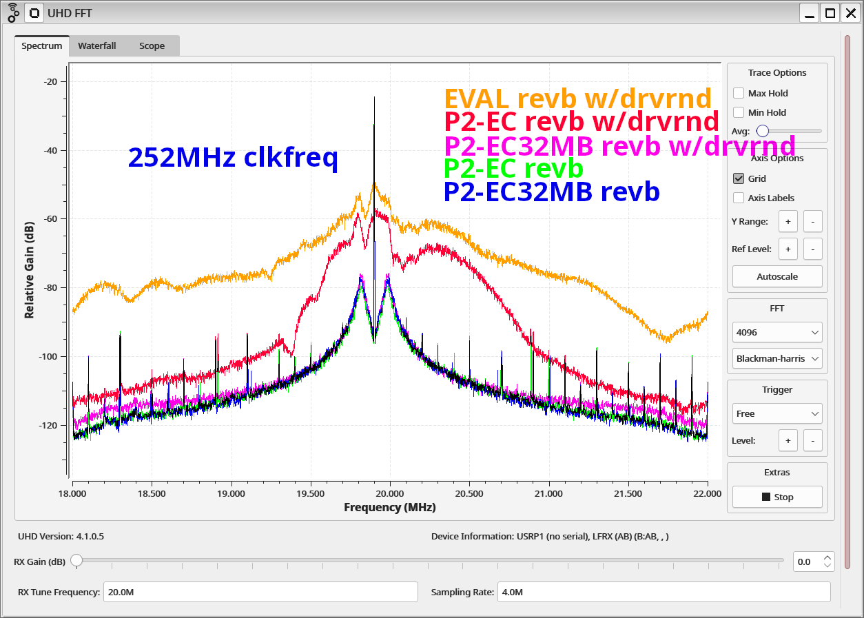
I was wondering if this would affect my radio transmitter code. It certainly does. An FM signal turns to static on affected boards.
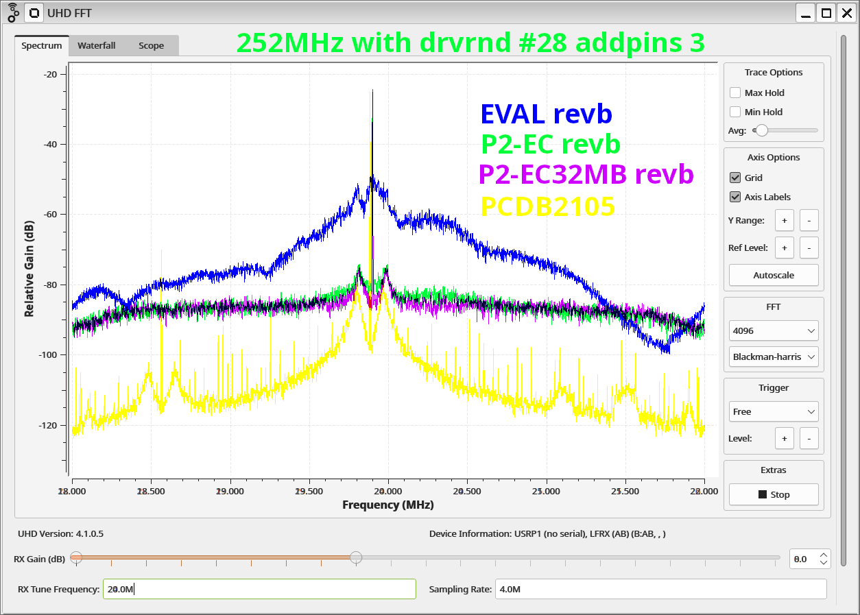
The P2-EC revb is is better than the eval but also fails when P28-P31 are stressed. The P2-EC32MB revb is unaffected by PLL related issues but a lot of random noise from those toggling pins is coupled into the signal. I could see this in the VGA signal too. I have the breadboard breakout board.
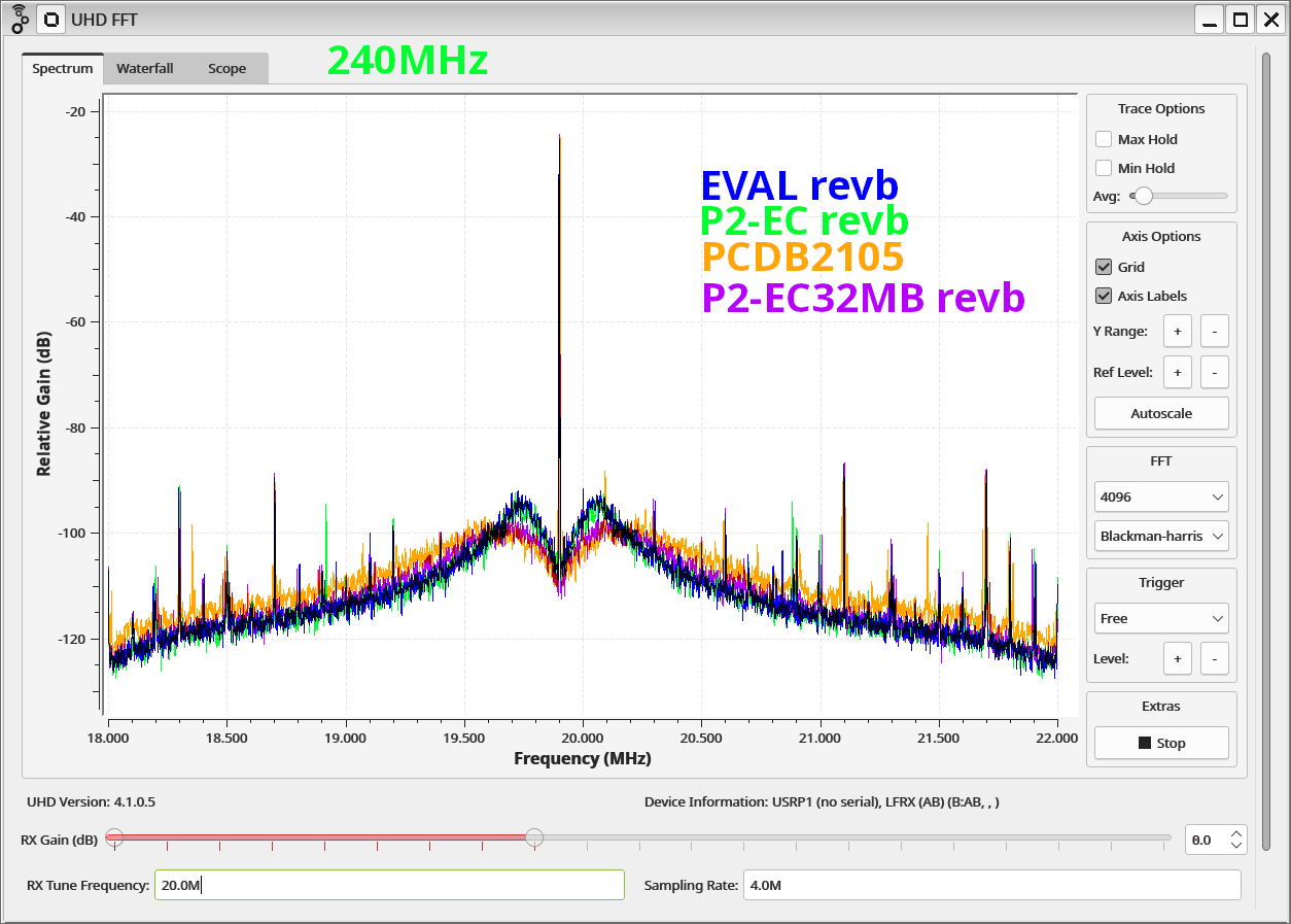
Is there anything fundamentally wrong with the P2 crystal oscillator? I don't think so. I can't really tell much difference between the P2-EC32MB with oscillator and a reasonable crystal design. Note that the PCDB2105 is a 2 layer board and uses a 24 MHz crystal. It's plot doesn't look great here but the higher crystal frequency is spreading the noise out over a wider area. I'm mostly interested in how high the humps are on each side of the generated signal. If you care about phase noise, use an integer multiple of the crystal frequency. That way the divider is 1 and the phase detector frequency is as high as possible. Changing from 252 MHz to 240 MHz dropped those humps by about 20 dB.
The EC32MBs were a later design and all its revisions use an external oscillator chip. The Edge-EC revA and revB are similar to Eval but given the improvement in your first graph, compared to the Eval, I'd guess the EC revB, at least, has space between the XO/XI tracks.
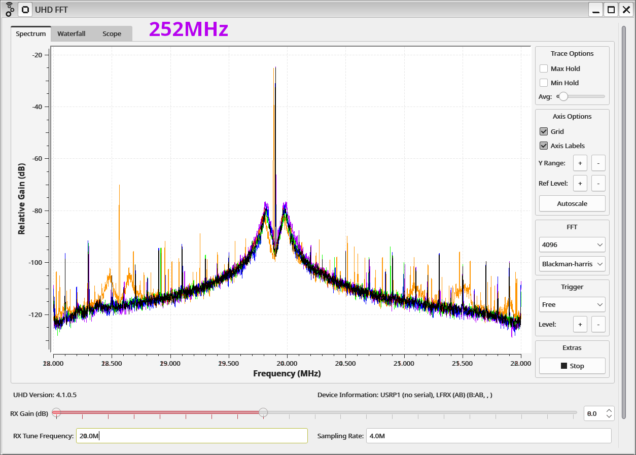
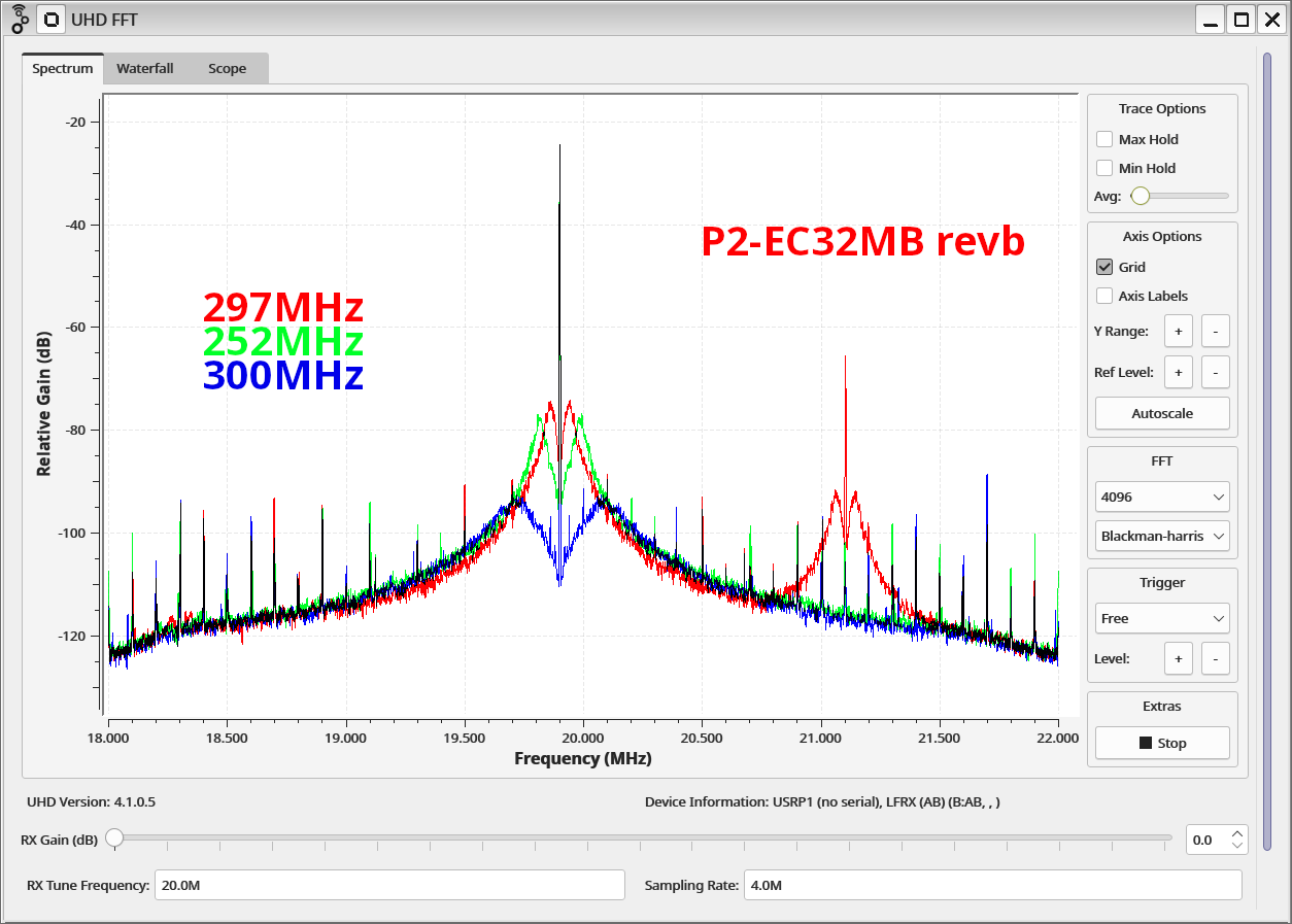
The difference between your second and third graphs backs up a number of other prior observations with VGA shimmering and I've shown it on a scope with clock jitter measuring too. Low divider values are better than high dividers. More specifically, low D divider. High P divider is fine because its outside the PLL's VCO control loop.
For digital or HD analogue video, a 12.0 MHz oscillator would be superior to 20.0 MHz . Former better for 252 MHz sysclk (D=1 vs. 5), same for 270 MHz (D = 2) , better for 297 MHz (D = 4 vs. 20) and same for 300 MHz (D = 1).
252 has far more divisors (/2, /3, /4, /6, /7, /9/, /12, ...) than 250, which makes 252 MHz perfect if sub-clocks of say 3.5, 4, 6 or 7 MHz are wanted. Also, 252 MHz is a standard DVI/HDMI frequency, again preferable for HDMI audio.
Monitors have no issue with locking to any dot clock. The so called standard is only a reference number. Frame rates are easily maintained by adjusting the blanking to suit. Audio will fit to the frame rate too. Or in the case of DisplayPort, or HDMI 2.1, data packet transfers there is no dot clock at all. It's a case of send the whole frame in a flash then pause until the next frame is due then repeat.
EDIT: Or DP could be a packet per line. I've not actually looked at the details. It's still no dot clock. Just have to fit the line rate instead of frame rate.
Point is 252 MHz is only a reference to define the line and frame rates. Adjusting the blanking to achieve the same using a different dot clock is just as good.
That's a half-truth. Native HDMI/DVI devices (presumably also DP) will just lock onto whatever you give them. But if you e.g. put a VGA converter box in the middle, it will copy the timing from the input 1:1, which can be far beyond the range of what any normal monitor can adjust to. Though that's mostly a limitation of the monitor firmware, the actual analog frontends have much wider parameter range.
Looking at the common factors between different clocks...
(phase comparator frequency for 20MHz crystal) [phase comparator frequency for 12MHz crystal]
252 = 2 * 2 * 3 * 3 * 7 (4MHz) [12MHz]
270 = 2 * 3 * 3 * 3 * 5 (10MHz) [6MHz]
297 = 3 * 3 * 3 * 11 (1MHz) [3MHz]
300 = 2 * 2 * 3 * 5 * 5 (20MHz) [12MHz]
20 = 2 * 2 * 5
12 = 2 * 2 * 3
If we wanted to generate a 1080p signal, the pixel clock is 148.5MHz. Double that and we get a sysclock of 297MHz. Unfortunately I expect the performance at 297MHz to be BAD. For video a 54MHz oscillator would be optimal with 27MHz a close second. 18MHz would work pretty well too. I'll check the phase noise at 297MHz on Monday.
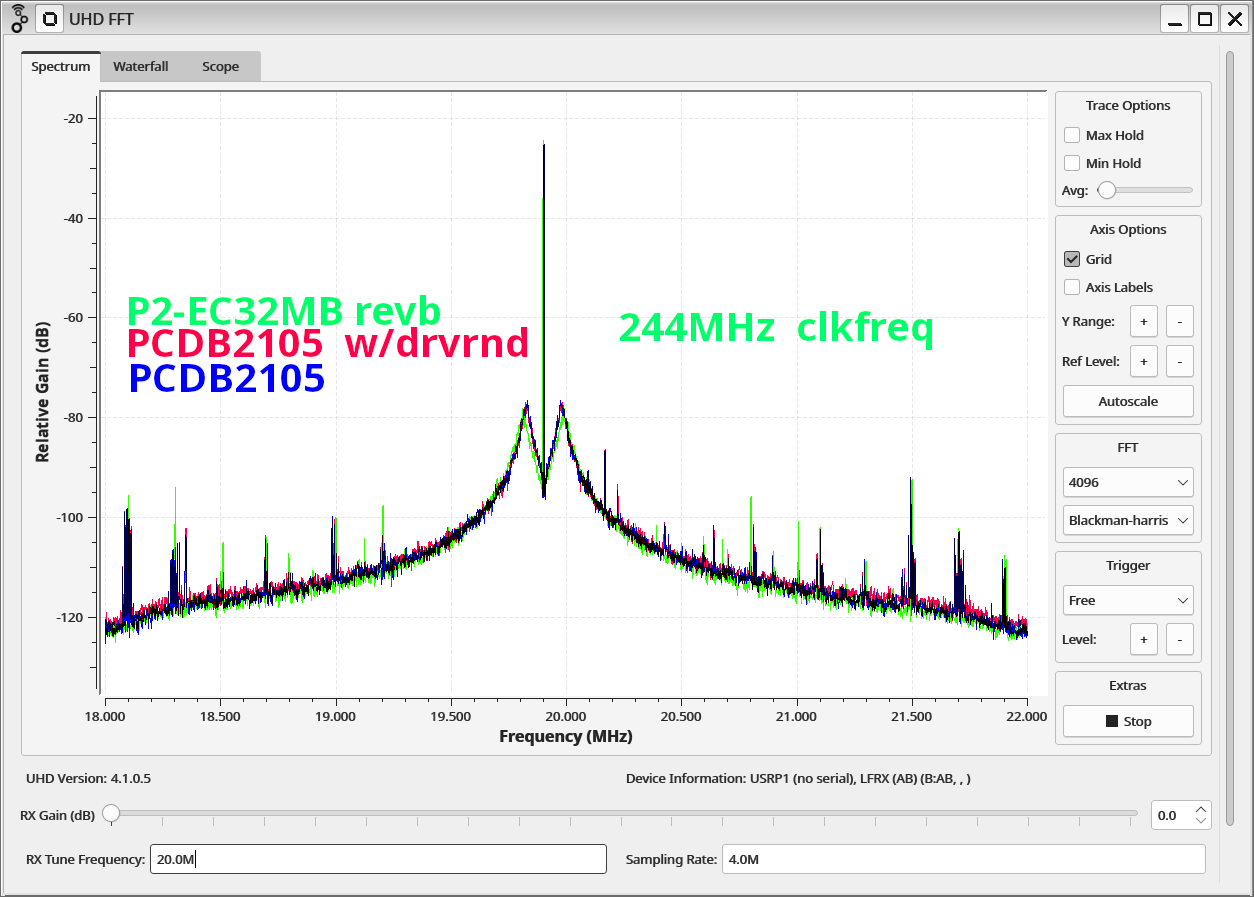
Note: in my post above, plots 1 and 2 use the same binary regardless of 20 or 24 MHz crystal. So the PCDB2105 is running at 302.4MHz and outputting 23.88MHz instead of 19.9MHz. In the third plot all boards ran at 240MHz which is an integer multiple of both clocks. My choice of 24 MHz was due to having an abundant supply of 24MHz crystals and not due to any PLL considerations.
With tape over P28-P31. Now we can see what's happening.
297 MHz is only slightly worse than 252MHz. That is an image at 21.1MHz. 297-19.9 = 277.1 277.1 - (64*4) = 21.1 The USRP1 has a 64MHz ADC clock.
At 244 MHz both 20 and 24 MHz clocks must be divided down to 4 MHz and then multiplied by 61. Looks like a crystal is fine. Looks fine on the plots and no audible artifacts on the radio signal. I have NOT checked VGA on this board.


Comments
Chip,
Exactly where does the internal clock circuits tap into the crystal oscillator loop?
There is a sense inverter on XI that feeds the PLL. Should have put a Schmitt in like JMG said to.
Meh. Cut yourself some slack, Chip. So much of the P2 was done darned near perfectly. Besides, there is always the P3! Encore?")
That's what I was expecting. And in the docs it says this of the XI source select:
It seems there is at least the desire to also have XI as a clock input other than crystal feedback.
However, I've now soldered wires onto the XI input and GND on an Eval Board and tested The 1 MHz to XI looks good on the scope. By commenting out said HUBSET, the Prop2 under test comes back to life - running from RCFAST. So I haven't killed the chip yet.
 ")
HUBSET #%00_10with a 1 MHz square wave inputted but, sadly, no action from the Prop2.PS: Here's the DUT source code:
dat org hubset #%00_10 'XI input from external clock gen rep @.rend, #0 drvnot #56 'toggle pin P56 waitx ##1_000_000 .rendbut CC=%00 disables the Xtal amplifier and it disables the XI buffer,
Docs state : %00 XI ignored
Your comment XI input from external clock gen is wishful thinking, not what actually happens in HW")
so you need anything above %00 to activate XI
I think the docs need changed too. There is too much hinting at %00 having a function, when it has none at all.
It does have a function")
It powers everything down, ie both the XI-XO Osc amplifier and the XI buffer amplifier so the Icc does not care what level those pins have.
The Xtal buffer draws significant current in the linear region.
That's XO, not XI.
There are two buffers in any Xtal oscillator.
One between XI-XO that activates the crystal, but there is another buffer, often overlooked, that has to take the sine wave, and square it up.
That buffer needs to also be disabled, if you want low power from the pins (or you need to drive XI to a known digital level)
I guess Chip could have added a light pulldown to XI, and kept the XI buffer enabled, as an alternate power saving approach, but that was not done.
Something to clarified in the docs.
When mode %00 is selected, the inverter and feedback resistor are turned off and XI is disconnected from the sense inverter (which should have been a Schmitt trigger).
Thanks. I've added a small comment to the silicon doc saying that %CC = %01 is required with an external clock source.
I was wondering if this would affect my radio transmitter code. It certainly does. An FM signal turns to static on affected boards.
The P2-EC revb is is better than the eval but also fails when P28-P31 are stressed. The P2-EC32MB revb is unaffected by PLL related issues but a lot of random noise from those toggling pins is coupled into the signal. I could see this in the VGA signal too. I have the breadboard breakout board.
Is there anything fundamentally wrong with the P2 crystal oscillator? I don't think so. I can't really tell much difference between the P2-EC32MB with oscillator and a reasonable crystal design. Note that the PCDB2105 is a 2 layer board and uses a 24 MHz crystal. It's plot doesn't look great here but the higher crystal frequency is spreading the noise out over a wider area. I'm mostly interested in how high the humps are on each side of the generated signal. If you care about phase noise, use an integer multiple of the crystal frequency. That way the divider is 1 and the phase detector frequency is as high as possible. Changing from 252 MHz to 240 MHz dropped those humps by about 20 dB.
The EC32MBs were a later design and all its revisions use an external oscillator chip. The Edge-EC revA and revB are similar to Eval but given the improvement in your first graph, compared to the Eval, I'd guess the EC revB, at least, has space between the XO/XI tracks.
The difference between your second and third graphs backs up a number of other prior observations with VGA shimmering and I've shown it on a scope with clock jitter measuring too. Low divider values are better than high dividers. More specifically, low D divider. High P divider is fine because its outside the PLL's VCO control loop.
For digital or HD analogue video, a 12.0 MHz oscillator would be superior to 20.0 MHz . Former better for 252 MHz sysclk (D=1 vs. 5), same for 270 MHz (D = 2) , better for 297 MHz (D = 4 vs. 20) and same for 300 MHz (D = 1).
I'd just use 250 MHZ instead of 252 MHz. And 300 MHz instead of 297 MHz. Tweak the blanking and you get the same syncs as original.
252 has far more divisors (/2, /3, /4, /6, /7, /9/, /12, ...) than 250, which makes 252 MHz perfect if sub-clocks of say 3.5, 4, 6 or 7 MHz are wanted. Also, 252 MHz is a standard DVI/HDMI frequency, again preferable for HDMI audio.
Monitors have no issue with locking to any dot clock. The so called standard is only a reference number. Frame rates are easily maintained by adjusting the blanking to suit. Audio will fit to the frame rate too. Or in the case of DisplayPort, or HDMI 2.1, data packet transfers there is no dot clock at all. It's a case of send the whole frame in a flash then pause until the next frame is due then repeat.
EDIT: Or DP could be a packet per line. I've not actually looked at the details. It's still no dot clock. Just have to fit the line rate instead of frame rate.
Point is 252 MHz is only a reference to define the line and frame rates. Adjusting the blanking to achieve the same using a different dot clock is just as good.
That's a half-truth. Native HDMI/DVI devices (presumably also DP) will just lock onto whatever you give them. But if you e.g. put a VGA converter box in the middle, it will copy the timing from the input 1:1, which can be far beyond the range of what any normal monitor can adjust to. Though that's mostly a limitation of the monitor firmware, the actual analog frontends have much wider parameter range.
Looking at the common factors between different clocks...
(phase comparator frequency for 20MHz crystal) [phase comparator frequency for 12MHz crystal]
252 = 2 * 2 * 3 * 3 * 7 (4MHz) [12MHz]
270 = 2 * 3 * 3 * 3 * 5 (10MHz) [6MHz]
297 = 3 * 3 * 3 * 11 (1MHz) [3MHz]
300 = 2 * 2 * 3 * 5 * 5 (20MHz) [12MHz]
20 = 2 * 2 * 5
12 = 2 * 2 * 3
If we wanted to generate a 1080p signal, the pixel clock is 148.5MHz. Double that and we get a sysclock of 297MHz. Unfortunately I expect the performance at 297MHz to be BAD. For video a 54MHz oscillator would be optimal with 27MHz a close second. 18MHz would work pretty well too. I'll check the phase noise at 297MHz on Monday.
Note: in my post above, plots 1 and 2 use the same binary regardless of 20 or 24 MHz crystal. So the PCDB2105 is running at 302.4MHz and outputting 23.88MHz instead of 19.9MHz. In the third plot all boards ran at 240MHz which is an integer multiple of both clocks. My choice of 24 MHz was due to having an abundant supply of 24MHz crystals and not due to any PLL considerations.
Hi @SaucySoliton
Do you happen to have the P2-EC Rev D?
No. I got the P2-EC rev B in a mystery box.
When I test again I will tape over P28-P31 contacts so the noise isn't coupled into the JonnyMac breadboard.
With tape over P28-P31. Now we can see what's happening.
297 MHz is only slightly worse than 252MHz. That is an image at 21.1MHz. 297-19.9 = 277.1 277.1 - (64*4) = 21.1 The USRP1 has a 64MHz ADC clock.
At 244 MHz both 20 and 24 MHz clocks must be divided down to 4 MHz and then multiplied by 61. Looks like a crystal is fine. Looks fine on the plots and no audible artifacts on the radio signal. I have NOT checked VGA on this board.