This test fails on P2-EVAL but is fine on RetroBlade2 (VGA on pins P0-4). I used the same binary for both tests.
It displays VGA 1280x1024 with text at 160x85.
It fails at 297MHz and 325MHz - haven't tried any other frequencies.
It is so bad that the monitor loses sync regularly.
Basically, this is Chips VGA demo code, modified to allow the VGA basepin to also reside on 4 pin groups with VS one pin below the basepin.
Then I added @rogloh killpll routine.
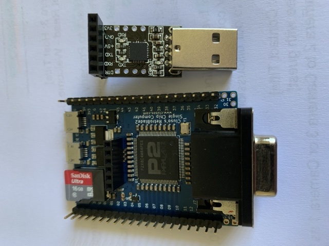
Warning: Please note there is something wrong between the CP2102 and loadp2 so if you're trying this on a RetroBlade2 you will need to use a PropPlug or an FT232RL usb/ttl.
The problem is that when you get a few pins toggling at the same time on P28-P31, the current draws are so sharp that it creates a sub-nanosecond brownout on those pins' internal GND and VIO busses. Those busses also power the XI and XO pins, which, when operating a crystal, are slewing at only 100mV/nanosecond. This brownout disrupts the input logic threshold of the XI sensor, causing extra pulses to be input to the PLL circuit, throwing it off. The PLL is quite protected, running off a heavily-filtered internal 1.8V supply, regulated from VIO. So, to solve this problem, only sharper transitions are needed on XI. An oscillator will provide this.
More bypass caps won't help, though very short traces on P28-P31 could possibly help by reducing the capacitive load.
If you don't use the default high-speed logic output modes on P28-P31, you will never see this problem.
@cgracey said:
The problem is that when you get a few pins toggling at the same time on P28-P31, the current draws are so sharp that it creates a sub-nanosecond brownout on those pins' internal GND and VIO busses. Those busses also power the XI and XO pins, which, when operating a crystal, are slewing at only 100mV/nanosecond. This brownout disrupts the input logic threshold of the XI sensor, causing extra pulses to be input to the PLL circuit, throwing it off. The PLL is quite protected, running off a heavily-filtered internal 1.8V supply, regulated from VIO. So, to solve this problem, only sharper transitions are needed on XI. An oscillator will provide this.
More bypass caps won't help, though very short traces on P28-P31 could possibly help by reducing the capacitive load.
If you don't use the default high-speed logic output modes on P28-P31, you will never see this problem.
Sorry Chip. My RetroBlade uses a crystal. The basic only difference is that I have proper bypass caps and bulk caps on both the 3V3 and 1V8 rails. I do not have this problem on my boards. I've been trying to tell you this for months. Why don't you consider this! You have my boards so you can try it out for yourself.
I bet if you try it on a P2D2 you will also find that this board does not suffer from the problem either because Peter also uses proper bypass and bulk capacitors. A 4u7F is not a bypass cap, and does not have enough bulk capacitance either when it is alone.
Like I've said, solder 100nF caps on top of the 4u7F to try it out. But you need to increase the 4u7F caps when they are the sole caps on a rail, like you have on the separate supplies to each set of power pins.
Von Sarvas and I did piggyback some much smaller caps onto the existing 4.7uF caps and it did not seem to have any effect.
Could it be that your Retroblade and Peter's P2D2 have shorter traces with less parasitic capacitance than either the P2 Eval or P2 Edge?
I know you've been talking about this for some time and because of that, Von Sarvas and I have reviewed our designs and even tried adding smaller caps to remedy this problem.
Ah, I need to explain what we realized when using a 1.5GHz scope the other day to study this apparent PLL problem. During the P28-P31 pin toggling, which was causing the PLL to jitter, the noise across the GND and V2831 supplies was only 40mV, due to our existing bypass caps, while the noise on the internal power supply lines, judging from the toggling P28-P31 pins and XI, was about 250mV! It doesn't matter what kind or how much bypass capacitance you put on the outside of the chip, it cannot overcome the internal power noise which causes the extra toggling on the XI sensor.
The only ways to overcome this problem is to either give sharper edges into XI (use an oscillator) or avoid toggling multiple P28-P31 logic pins simultaneously.
Chip, bypass and bulk capacitors are there to keep the internal supplies as stable as possible. If you don’t do that, (and neither your P2-EVAL nor P2-EDGE do this) then you will never be able to keep the internal lines stable. My RetroBlade is overkill, but the proof is in the pudding.
Many non-prop designs suffered similar problems with SD interfaces because the board designers didn’t understand basic power supply design. The SD cards generate power spikes, and without the bulk and bypass caps at the socket pins, there were many problems. I have always put a 10uF tantalum and 100nF right at the socket pins. These days, the monos are really good, so on the RetroBlade2 I used a 4u7F and a 100nF mono at the socket pins. As I’ve said before, there is even the school of thought that 10nF bypass caps should also be included. And of course the type is important too.
As you know, I’m not a fan of your separate supplies to each pin block because you cannot easily get decent bypass and bulk caps at the pins. IMHO (ie opinion only) a single supply with good tracks and plenty of bulk and bypass caps would work better.
I’ve asked you to try my board with your ADC as I think you might obtain better results. I don’t have the gear to test this out.
@cgracey said:
Could it be that your Retroblade and Peter's P2D2 have shorter traces with less parasitic capacitance than either the P2 Eval or P2 Edge?
I know the P2D2 is very small board ... and I now see the RetroBlade2 is too. And Cluso does have an awful lot of capacitors on the power rails.
@"Peter Jakacki" said:
Just loaded video.binary onto a P2D2r4 and it is rock solid and clean. Had to use loadp2.py though.
Curiously I had to use an FT232RL with loadp2. Something has changed on my pc lately. I had been trying to track down problems with pnut and the CP2102, and now that it works, loadp2 doesn’t. I suspect the driver may have changed as working code will no longer download with the loadp2 and CP2102 combo. Currently I don’t have the time to chase it through so it will have to wait.
@cgracey said:
Could it be that your Retroblade and Peter's P2D2 have shorter traces with less parasitic capacitance than either the P2 Eval or P2 Edge?
I know the P2D2 is very small board ... and I now see the RetroBlade2 is too. And Cluso does have an awful lot of capacitors on the power rails.
Yes. There are 8 * 100nF 0603 X7R bypass caps down each side of the P2, right on the power pins. At the ends are 4u7F bulk caps in the three corners. And there is 22uF and 100nF directly on the output of each regulator.
Yes, it's overkill. But hey, it works. And I can always leave some of the caps off in a later build.
@"Peter Jakacki" said:
Just loaded video.binary onto a P2D2r4 and it is rock solid and clean. Had to use loadp2.py though.
What is it about loadp2 that is having issues with both the P2D2 and Cluso's RetroBlade when downloading large binaries?
I have no issues here on P2-EVAL with downloading this larger image size, though I am using the P2-EVAL on a Mac.
@rogloh said:
What is it about loadp2 that is having issues with both the P2D2 and Cluso's RetroBlade when downloading large binaries?
I have no issues here on P2-EVAL with downloading this larger image size, though I am using the P2-EVAL on a Mac.
Cluso99 is using CP2102 and I'm using a micro that appears as a CP2102 whereas the P2-EVAL is using the FT232R. I believe there is a problem with the Silabs drivers and the method of setting baud rates beyond 1Mbd
@"Peter Jakacki" said:
I had tried the drvnot before trying drvrnd, but no difference. However, I will run it again.
Well, given the P2D2 has far less VIO supply caps, it looks like, as Chip has indicated already, what makes the difference is the I/O pin capacitive loading. The Eval Board has longish I/O tracks that run inside the PCB sandwiched between two ground layers.
I just put 470pF onto P28 just for a quick test but that didn't make one iota of difference. I could try all 4 pins but i don't expect to see any problems because there is no way that the track capacitance is anywhere near that figure. Has anyone piggybacked a 104 or 103 onto that 475? I know I looked at the datasheets for that cap and while bulk capacitance is fine, it is no replacement for the characteristics of the smaller caps which btw are many in parallel on our boards. Much less ESR than even a single one and overall bypass and bulk capacitance to boot.
BTW, the forums has had lots of good advice on many hardware matters. The first eval board had really long tracks to the other side of the board for the SD etc. Many of these problems due to empirical guesses could easily have been avoided and as I have always said, having extra footprints for options or alternatives are never bad.
Ooops, I had the cap in the wrong place. Put it back properly and now get P28..31 to output 1/2 clkfreq. TAQOZ# 28 4 PINS $8000_0000 NCO --- ok
Nada, even with the 470pF sitting there. Also tried other frequencies and all pins etc. TAQOZ# .CLK --- 325MHz ok
Now, how about a random sweep on all 8 pins. TAQOZ# BEGIN 24 8 ADO I PIN RND NCO LOOP 5 ms KEY UNTIL ---
Nada nada nada nada. (The scope goes crazy though).
Have you guys ever looked at the x86 chips built on fibreglass slivers (very fine pcbs). There are large numbers of bypass capacitors (and probably bulk) on those chips/boards. If you don’t know why, have you at least wondered why?
I designed my board to be quiet and simple. I wanted to be able to overclock without over stressing my circuit. I did not use switching regulators, nor massive 2oz copper as I was quite happy to be somewhat restricted below the total maximum power the P2 can consume.
My board (and neither does Peter’s P2D2) exhibit the problems seen on the two Parallax boards. Our boards do not use special techniques to obtain these better results, just good engineering design practices.
Rather than try and find some quirk that explains why you’re seeing problems on your designs, why not look and listen at what we did?
Chip, you have both our boards for comparisons. I have no idea what is inside the P2, but I do know if you don’t give it proper power from the outside, then the inside is likely not to work properly too. Isn’t this problem just a manifestation of the outside causing the inside problem!!!
I say again, the outside power at your power and ground rails (pins) is not providing sufficient bulk capacitance and bypass capacitance to squelch the switching spikes and deliver the current peaks as and when required. This is electronic design 101, pure and simple. Your problem is caused by one or both of these deficiencies. A regulator cannot provide for these inadequacies.
@evanh
You mentioned my board is smaller and therefore has shorter traces. I presume you mean P28-31 traces?
If so, my traces go to the edge connector 0.1" pitch, and also to the VGA connector, which is soldered in so the connector too is attached to these pins. This is not the difference causing/solving the problem.
I'm seeing the same thing as @Cluso99 I think. VGA is fine with my board, but all messed up with Eval board.
Update: Same result with Rev.3B of this board.
This is kind of hard to believe as my board is just 2 layer and nowhere near as professionally made, but there it is.
Here's what the area around my crystal looks like (see attached).
Maybe it's just how the crystal is very close to P2 chip with nothing else within the perimeter of crystal traces?
Thanks for trying this Ray and pleased its working on your board too.
Looks like you’re using an oscillator.
But that’s not the problem - it’s power related.
Reduce the parasitic capacitance between XTALIN and XTALOUT pins by routing them as far apart
as possible
This and my limited knowledge on the subject makes me think the traces are too close together.
I'm tempted to cut one of the traces and use a jumper instead.
Don't want to mess up my Eval board though


Comments
This test fails on P2-EVAL but is fine on RetroBlade2 (VGA on pins P0-4). I used the same binary for both tests.
It displays VGA 1280x1024 with text at 160x85.
It fails at 297MHz and 325MHz - haven't tried any other frequencies.
It is so bad that the monitor loses sync regularly.
Basically, this is Chips VGA demo code, modified to allow the VGA basepin to also reside on 4 pin groups with VS one pin below the basepin.
Then I added @rogloh killpll routine.
Warning: Please note there is something wrong between the CP2102 and loadp2 so if you're trying this on a RetroBlade2 you will need to use a PropPlug or an FT232RL usb/ttl.
The problem is that when you get a few pins toggling at the same time on P28-P31, the current draws are so sharp that it creates a sub-nanosecond brownout on those pins' internal GND and VIO busses. Those busses also power the XI and XO pins, which, when operating a crystal, are slewing at only 100mV/nanosecond. This brownout disrupts the input logic threshold of the XI sensor, causing extra pulses to be input to the PLL circuit, throwing it off. The PLL is quite protected, running off a heavily-filtered internal 1.8V supply, regulated from VIO. So, to solve this problem, only sharper transitions are needed on XI. An oscillator will provide this.
More bypass caps won't help, though very short traces on P28-P31 could possibly help by reducing the capacitive load.
If you don't use the default high-speed logic output modes on P28-P31, you will never see this problem.
Sorry Chip. My RetroBlade uses a crystal. The basic only difference is that I have proper bypass caps and bulk caps on both the 3V3 and 1V8 rails. I do not have this problem on my boards. I've been trying to tell you this for months. Why don't you consider this! You have my boards so you can try it out for yourself.
I bet if you try it on a P2D2 you will also find that this board does not suffer from the problem either because Peter also uses proper bypass and bulk capacitors. A 4u7F is not a bypass cap, and does not have enough bulk capacitance either when it is alone.
Like I've said, solder 100nF caps on top of the 4u7F to try it out. But you need to increase the 4u7F caps when they are the sole caps on a rail, like you have on the separate supplies to each set of power pins.
Von Sarvas and I did piggyback some much smaller caps onto the existing 4.7uF caps and it did not seem to have any effect.
Could it be that your Retroblade and Peter's P2D2 have shorter traces with less parasitic capacitance than either the P2 Eval or P2 Edge?
I know you've been talking about this for some time and because of that, Von Sarvas and I have reviewed our designs and even tried adding smaller caps to remedy this problem.
Ah, I need to explain what we realized when using a 1.5GHz scope the other day to study this apparent PLL problem. During the P28-P31 pin toggling, which was causing the PLL to jitter, the noise across the GND and V2831 supplies was only 40mV, due to our existing bypass caps, while the noise on the internal power supply lines, judging from the toggling P28-P31 pins and XI, was about 250mV! It doesn't matter what kind or how much bypass capacitance you put on the outside of the chip, it cannot overcome the internal power noise which causes the extra toggling on the XI sensor.
The only ways to overcome this problem is to either give sharper edges into XI (use an oscillator) or avoid toggling multiple P28-P31 logic pins simultaneously.
Just loaded video.binary onto a P2D2r4 and it is rock solid and clean. Had to use loadp2.py though.
Chip, bypass and bulk capacitors are there to keep the internal supplies as stable as possible. If you don’t do that, (and neither your P2-EVAL nor P2-EDGE do this) then you will never be able to keep the internal lines stable. My RetroBlade is overkill, but the proof is in the pudding.
Many non-prop designs suffered similar problems with SD interfaces because the board designers didn’t understand basic power supply design. The SD cards generate power spikes, and without the bulk and bypass caps at the socket pins, there were many problems. I have always put a 10uF tantalum and 100nF right at the socket pins. These days, the monos are really good, so on the RetroBlade2 I used a 4u7F and a 100nF mono at the socket pins. As I’ve said before, there is even the school of thought that 10nF bypass caps should also be included. And of course the type is important too.
As you know, I’m not a fan of your separate supplies to each pin block because you cannot easily get decent bypass and bulk caps at the pins. IMHO (ie opinion only) a single supply with good tracks and plenty of bulk and bypass caps would work better.
I’ve asked you to try my board with your ADC as I think you might obtain better results. I don’t have the gear to test this out.
Cluso,
Put this in your test on the RetroBlade2.
PUB killpll() | pllpins pllpins := 28 addpins 3 org rep #1, #0 drvnot pllpins endI know the P2D2 is very small board ... and I now see the RetroBlade2 is too. And Cluso does have an awful lot of capacitors on the power rails.
If you look at the code in #68 you will see I have this")
I changed one line. Give it a try.
Curiously I had to use an FT232RL with loadp2. Something has changed on my pc lately. I had been trying to track down problems with pnut and the CP2102, and now that it works, loadp2 doesn’t. I suspect the driver may have changed as working code will no longer download with the loadp2 and CP2102 combo. Currently I don’t have the time to chase it through so it will have to wait.
I also tried this from inside TAQOZ @325MHz with a KILLPLL function. I loaded a 640x480 image, then switched to 720p and drove the 4 pins with KILLPLL
I then verified it was doing a drvrnd on those pins which it was. What does that tell us?
Yes. There are 8 * 100nF 0603 X7R bypass caps down each side of the P2, right on the power pins. At the ends are 4u7F bulk caps in the three corners. And there is 22uF and 100nF directly on the output of each regulator.
Yes, it's overkill. But hey, it works. And I can always leave some of the caps off in a later build.
FYI P2D2 and RetroBlade2 are both 2-layer 1oz.
Cluso,
Try that code I posted. It's a one line change from your code. Peter, you can too. I changed DRVRND to DRVNOT.
I can see the difference between DRVRND and DRVNOT on the scope with my testing. DRVNOT has a stronger effect.
Oh. I didn’t see the subtle change. Might not get a chance to try it for 24hrs.
I had tried the drvnot before trying drvrnd, but no difference. However, I will run it again.
What is it about loadp2 that is having issues with both the P2D2 and Cluso's RetroBlade when downloading large binaries?
I have no issues here on P2-EVAL with downloading this larger image size, though I am using the P2-EVAL on a Mac.
Cluso99 is using CP2102 and I'm using a micro that appears as a CP2102 whereas the P2-EVAL is using the FT232R. I believe there is a problem with the Silabs drivers and the method of setting baud rates beyond 1Mbd
Well, given the P2D2 has far less VIO supply caps, it looks like, as Chip has indicated already, what makes the difference is the I/O pin capacitive loading. The Eval Board has longish I/O tracks that run inside the PCB sandwiched between two ground layers.
I just put 470pF onto P28 just for a quick test but that didn't make one iota of difference. I could try all 4 pins but i don't expect to see any problems because there is no way that the track capacitance is anywhere near that figure. Has anyone piggybacked a 104 or 103 onto that 475? I know I looked at the datasheets for that cap and while bulk capacitance is fine, it is no replacement for the characteristics of the smaller caps which btw are many in parallel on our boards. Much less ESR than even a single one and overall bypass and bulk capacitance to boot.
BTW, the forums has had lots of good advice on many hardware matters. The first eval board had really long tracks to the other side of the board for the SD etc. Many of these problems due to empirical guesses could easily have been avoided and as I have always said, having extra footprints for options or alternatives are never bad.
Ooops, I had the cap in the wrong place. Put it back properly and now get P28..31 to output 1/2 clkfreq.
TAQOZ# 28 4 PINS $8000_0000 NCO --- okNada, even with the 470pF sitting there. Also tried other frequencies and all pins etc.
TAQOZ# .CLK --- 325MHz okNow, how about a random sweep on all 8 pins.
TAQOZ# BEGIN 24 8 ADO I PIN RND NCO LOOP 5 ms KEY UNTIL ---Nada nada nada nada. (The scope goes crazy though).
Have you guys ever looked at the x86 chips built on fibreglass slivers (very fine pcbs). There are large numbers of bypass capacitors (and probably bulk) on those chips/boards. If you don’t know why, have you at least wondered why?
I designed my board to be quiet and simple. I wanted to be able to overclock without over stressing my circuit. I did not use switching regulators, nor massive 2oz copper as I was quite happy to be somewhat restricted below the total maximum power the P2 can consume.
My board (and neither does Peter’s P2D2) exhibit the problems seen on the two Parallax boards. Our boards do not use special techniques to obtain these better results, just good engineering design practices.
Rather than try and find some quirk that explains why you’re seeing problems on your designs, why not look and listen at what we did?
Chip, you have both our boards for comparisons. I have no idea what is inside the P2, but I do know if you don’t give it proper power from the outside, then the inside is likely not to work properly too. Isn’t this problem just a manifestation of the outside causing the inside problem!!!
I say again, the outside power at your power and ground rails (pins) is not providing sufficient bulk capacitance and bypass capacitance to squelch the switching spikes and deliver the current peaks as and when required. This is electronic design 101, pure and simple. Your problem is caused by one or both of these deficiencies. A regulator cannot provide for these inadequacies.
It's 1:00am here. Just got out of bed to try DRVNOT (at 325MHz)
RamBlade2 = perfect
P2-EVAL = no display at all - monitor cannot sync
@evanh
You mentioned my board is smaller and therefore has shorter traces. I presume you mean P28-31 traces?
If so, my traces go to the edge connector 0.1" pitch, and also to the VGA connector, which is soldered in so the connector too is attached to these pins. This is not the difference causing/solving the problem.
I just tried the code from Post #68 with both my board and P2 Eval board.
This is P2_Board_4A with the design files posted here: https://forums.parallax.com/discussion/170725/my-first-p2-pcb-its-finally-done/p1
I'm seeing the same thing as @Cluso99 I think. VGA is fine with my board, but all messed up with Eval board.
Update: Same result with Rev.3B of this board.
This is kind of hard to believe as my board is just 2 layer and nowhere near as professionally made, but there it is.
Here's what the area around my crystal looks like (see attached).
Maybe it's just how the crystal is very close to P2 chip with nothing else within the perimeter of crystal traces?
Thanks for trying this Ray and pleased its working on your board too.
Looks like you’re using an oscillator.
But that’s not the problem - it’s power related.
It's a crystal. Same as Eval board, I think:
PART: XC2464CT-ND
MFG : ECS Inc. (VA) / ECS-200-9-33B-CKY-TR
The other two ends are both connected to ground with vias.
Ok. I saw caps at one end and presumed they were power caps. I’m not at my computer so couldn’t check your schematics.
Wonder if the P2 Eval board's crystal traces are too close together...
I found this line in this: https://ww1.microchip.com/downloads/en/DeviceDoc/Atmel-8128-Best-Practices-for-the-PCB-Layout-of-Oscillators_ApplicationNote_AVR186.pdf
This and my limited knowledge on the subject makes me think the traces are too close together.")
I'm tempted to cut one of the traces and use a jumper instead.
Don't want to mess up my Eval board though