On my P2ME2 board I managed to design the PCB to work with a crystal by default (and I expect most use cases will be happy with a standard crystal) but it can also be fitted with an oscillator in case I see any jitter problems with the P2 with too much noise on the PLL supply.
To do this it just needs some pads for an optional bypass cap and a solder jumper that can be added and a track cut made so it turned out actually not that much of a difficult thing to add in at the board design stage and costs nothing but a tiny amount more PCB area. In my case, the issue will probably be finding a good oscillator that fits the crystal footprint (which is somewhat large these days vs the common oscillator sizes - there are so many sizes!), but that was my own choice to make things easier to hand solder...
Here's the idea, you just need a way to disconnect pin 1 from XO (track cut) and then feed power into pin 4 via the solder jumper if you use an oscillator (its bypass cap was on the other layer). I also made a tiny solder jumper near XO to be able to resurrect the trace after a cut if I change my mind too.
@ManAtWork said:
The topic here is how to make a simple evaluation and experimentation board. I won't discuss caesium clocks and other academic stuff, here. The crystal I use has 10ppm tolerance. If nobody convinces me that an oscillator is required for a standard application (for example, beacuse there is visible pixel jitter on an HDMI screen) then I'll keep the crystal. Serving 90% of the applications is anough for me. If 10% need a better clock they can always buy more expensive boards elsewhere.
Same thing for the USB/FTDI programmer. Some of the boards will only be used for development where you need a programmer all the time. But others will only be programmed once or few times and then will run stand-alone in the application. And some (as my servo and induction heating project) will even require isolated programming because they are connected to high voltage. So keeping the prog plug separate makes more sense to me. However I agree that a USB connector for +5V power is better than a screw terminal because it prevents most people from connecting the wrong voltage or polarity.
+1
Some want the Lamborghini but only want to use it for the local shopping, and pay the old VW price.
@ManAtWork said:
The topic here is how to make a simple evaluation and experimentation board. I won't discuss caesium clocks and other academic stuff, here. The crystal I use has 10ppm tolerance. If nobody convinces me that an oscillator is required for a standard application (for example, beacuse there is visible pixel jitter on an HDMI screen) then I'll keep the crystal. Serving 90% of the applications is anough for me. If 10% need a better clock they can always buy more expensive boards elsewhere.
Same thing for the USB/FTDI programmer. Some of the boards will only be used for development where you need a programmer all the time. But others will only be programmed once or few times and then will run stand-alone in the application. And some (as my servo and induction heating project) will even require isolated programming because they are connected to high voltage. So keeping the prog plug separate makes more sense to me. However I agree that a USB connector for +5V power is better than a screw terminal because it prevents most people from connecting the wrong voltage or polarity.
I'll add an SD card socket to the next revision. I prefer the slider lock type over the more common push/pull lock because the socket has a rectangular outline and can be centered and placed more reliably with my P&P machine. I have problems with the asymetric shape. I can't use mechanical centering jaws because they twist or knock the part off the nozzle and I can't use camera vision because the shiny stainless steel cover causes reflections.
If somebody knows a push/pull type that has a symetric rectangular shape and doesn't cost more than $0.50 please tell me.
@rogloh said:
On my P2ME2 board I managed to design the PCB to work with a crystal by default (and I expect most use cases will be happy with a standard crystal) but it can also be fitted with an oscillator in case I see any jitter problems with the P2 with too much noise on the PLL supply.
...
Yes, a great example of how easy it is, with some forethought, to cover both user choices in a PCB layout
The one I use has no lock, it’s just a push/pull type and has no metal frame but I don’t know how the pnp machine would pick it up without jaws. It’s C266612 from LCSC.
The smaller one I have used from mouser is much smaller and expensive.
@ManAtWork said:
I'll add an SD card socket to the next revision. I prefer the slider lock type over the more common push/pull lock because the socket has a rectangular outline and can be centered and placed more reliably with my P&P machine. I have problems with the asymetric shape. I can't use mechanical centering jaws because they twist or knock the part off the nozzle and I can't use camera vision because the shiny stainless steel cover causes reflections.
If somebody knows a push/pull type that has a symetric rectangular shape and doesn't cost more than $0.50 please tell me.
I'll take C266618. It has a flat top, rectangular outline without protuding tabs and gull wing pins accessible on the rear side (for optional hand soldering)
Thanks @jmg
Besides the uSD card socket, a nice one btw, do you plan any more significant changes to the KISS board ? Not that I would like to propose any. Just asking.
Do you plan to place the uSD on the flip side (bottom) ?
I presume you intend to have it assembled on the board too, right ?
Sounds good.
Makes me want the new KISS board or two.
If you could also keep the current KISS board in the "in production" status as an option for some time, maybe with that bigger flash chip... I just hate to see those excess, unused (version 1) boards totally wasted. Just a thought.
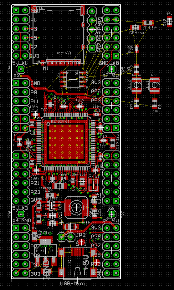
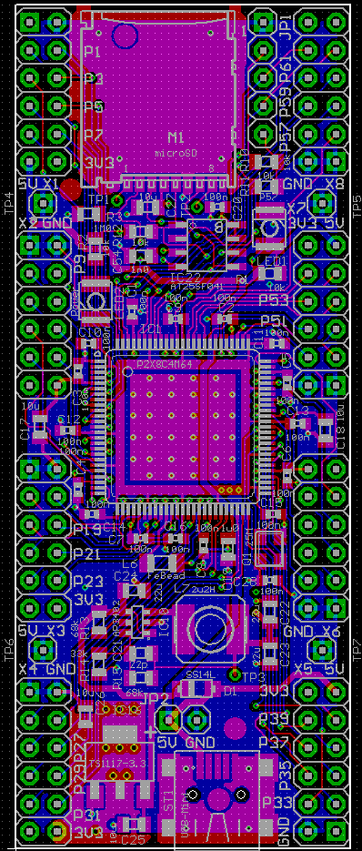
The SD card socket is HUGE. But I think it should fit, even on the top side. I have moved the LDO to the other side near the power connector, now USB.
Questions and comments about the SD card:
is the 4-bit mode (pins 1 and 8) really needed? It might allow faster data transfer after the initial boot process but does anybody use this?
I'll ignore the mechanical "card present" switch of the socket. I think presence can also be detected via software polling.
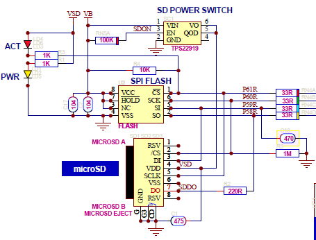
The P2 reference manual says the SD card has an internal pullup on P60 which is used to detect SD for booting. However, the pullup on P61 overrides this. So if anybody wants to boot (directly) from SD card instead of SPI flash then the pullup resistor on P61 has to be removed, right?
The P2D2 schematic has a weak pulldown on P60 (1M). I think this not really neccessary.
is the 4-bit mode (pins 1 and 8) really needed? It might allow faster data transfer after the initial boot process but does anybody use this? - even if nobody uses it right now, leaving off these would prevent an easy use in the future - I would save them.
I'll ignore the mechanical "card present" switch of the socket. I think presence can also be detected via software polling. - Good move.
The P2 reference manual says the SD card has an internal pullup on P60 which is used to detect SD for booting. However, the pullup on P61 overrides this. So if anybody wants to boot (directly) from SD card instead of SPI flash then the pullup resistor on P61 has to be removed, right? - Peter's TAQOZ boots directly from the SD, IIRC so either one needs to remove it or solder it. I'd opt for a soldering it in instead of removing it but that may not be convenient for other users.
The P2D2 schematic has a weak pulldown on P60 (1M). I think this is not really necessary. - You may be right but I suspect Peter has done some extensive testing and this resistor is there for a purpose, but this is just my speculation.
@ManAtWork said:
The SD card socket is HUGE. But I think it should fit, even on the top side. I have moved the LDO to the other side near the power connector, now USB.
Looks nice.
minor tweaks : rogloh managed a GND trace between the P2 data pin and XI and made the XI trace as short as possible, and has a cut/bridge choice on XO
He also moved inductor further from XI, so maybe SMPS cell can spin 180', to swap L and smps IC ?
@ManAtWork said:
Questions and comments about the SD card:
is the 4-bit mode (pins 1 and 8) really needed? It might allow faster data transfer after the initial boot process but does anybody use this?
I'll ignore the mechanical "card present" switch of the socket. I think presence can also be detected via software polling.
The P2 reference manual says the SD card has an internal pullup on P60 which is used to detect SD for booting. However, the pullup on P61 overrides this. So if anybody wants to boot (directly) from SD card instead of SPI flash then the pullup resistor on P61 has to be removed, right?
The P2D2 schematic has a weak pulldown on P60 (1M). I think this not really neccessary.
This is P2D2R5 SCH section
I'm rusty on the details, but IIRC there were some reset issues that the power switch resolved ? (ie power removal reset of the SD during P2 reset is not a bad idea ?)
@jmg said:
I'm rusty on the details, but IIRC there were some reset issues that the power switch resolved ? (ie power removal reset of the SD during P2 reset is not a bad idea ?)
That rings a bell... Was that a code issue that @Cluso99 since solved with a code update? A subtle combination of flash and sd usage could leave the sd card needing a powercycle...?
Ah, interesting. Do you have a link to the original discussion? What would be the consequences if I didn't implement the power switch? A little transistor wouldn't be a problem but I try to avoid the bigger power monitor IC peter put onto the P2D2. If it meant loosing the ability to boot from SD card I wouldn't care much. The SPI flash is always there so I don't mind using the SDC only for data storage.
BTW, I'll connect pins 1+8 to open test points. If somebody really needs QSPI mode he could connect them to P2 port pins with jumper wires.
I wouldn't swap the switching regulator IC and the inductor. The inductor has a noisy and a quiet side. The noisy side (left) is switched with fast edges and could couple to the XI input via stray capacitance. The quiet side (right) is facing towards the crystal and if effectively at a constant voltage. The magnetic field of a buck converter in continous current mode is also nearly constant so I don't expect much EMI. If I'm wrong we could use a shielded core inductor for sensitive applications.
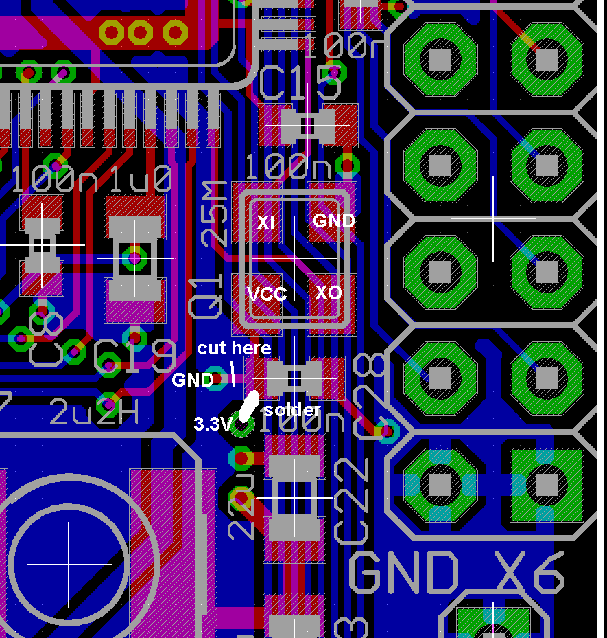
I had no space for real solder jumper pads but it should be possible to cut the trace from GND to pin 4 of the oscillator and solder a bridge to the adjacent via which is connected to 3.3V and has the solder mask open. Unfortunatelly, the P2 doesn't have a dedicated XI-only oscillator input mode so the XO pin trace has also to be cut.
@ManAtWork said:
Ah, interesting. Do you have a link to the original discussion? What would be the consequences if I didn't implement the power switch? A little transistor wouldn't be a problem but I try to avoid the bigger power monitor IC peter put onto the P2D2. If it meant loosing the ability to boot from SD card I wouldn't care much. The SPI flash is always there so I don't mind using the SDC only for data storage.
BTW, I'll connect pins 1+8 to open test points. If somebody really needs QSPI mode he could connect them to P2 port pins with jumper wires.
Can't find it. Cluso may recall.
In either case, I'd imagine the issue was with the SD card locking up (not the flash chip)... in which case, the user could remove/re-insert the SD card to resolve? Probably no need for an electronic switch at the KISS level.
@ManAtWork said:
I had no space for real solder jumper pads but it should be possible to cut the trace from GND to pin 4 of the oscillator and solder a bridge to the adjacent via which is connected to 3.3V and has the solder mask open. Unfortunatelly, the P2 doesn't have a dedicated XI-only oscillator input mode so the XO pin trace has also to be cut.
Yeah the cut is unavoidable. It's a pity that your C15 cap sort of gets in the way, otherwise you might be able to squeeze the xtal even closer in to get it really tight. Hopefully XI won't pickup too much noise from that bypass cap sitting right over it. Unlike my own two layer board, it looks like you'll be using a four layer board so the ground plane will help shield all those other signals on the layer below it.
I don’t use a switch. The issue in RevA chips was that there was a path where the SD card failed to release the DO pin which prevents the Flash from working. There is an obscure path in RevB that should not be hit but all other paths should clear down the SD correctly. My soft SD driver handles all cases AFAIK. if it ever becomes a problem then the loader could be changed to check for a stuck DO and issue the SD reset sequence before attempting to program the Flash.
So, in summary, I don’t believe a switch is necessary.
I also do not use R2, C18 or R5. R5 could be used if you want to be sure but the way I check for an SD card in the ROM boot code is to set the pin low and then tri state and read. If there is no pull-up (internal in the SD card) then this pin will read low due to the zero charge on the pin before it has time to float much. This is what Chip uses to check for Flash so I think it’s a safe bet. And I’ve not seen any issues and I use SD in and out often. The only issues are pnut’s reset timing.
OK, this is good news. So it should work the way it is, now. Here are the current schematic and layout.
And BTW, I don't like micro USB connectors. My kids frequently break the connectors of the mobile phone chargers and we have to buy new ones every half year or so. Mini USB plugs are much more durable.
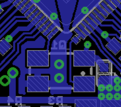
And yes, the board is 4-layer, of course. Otherwise I wouldn't dare to route so many signals below the crystal. The placement is really tight. I had to put some of the fiducials underneath the USB and SD sockets.
Next question: Do some USB hubs need pull/pulldown resistors on the data lines to enable power to the device?
If it's the same USB hub that powers the board and the USB>serial then I would think it's not relevant (if I'd used a USB hub that would be the same one). Otherwise I would use a power bank for power, so also irrelevant unless it's a USB-C capable power bank. But then it would start at 5V and then try to negotiate higher ?
@ManAtWork said:
The topic here is how to make a simple evaluation and experimentation board. I won't discuss caesium clocks and other academic stuff, here. The crystal I use has 10ppm tolerance. If nobody convinces me that an oscillator is required for a standard application (for example, beacuse there is visible pixel jitter on an HDMI screen) then I'll keep the crystal. Serving 90% of the applications is anough for me. If 10% need a better clock they can always buy more expensive boards elsewhere.
I have had plenty of designs using 10ppm crystals get 150ppm out because the loading capacitors aren't quite right. This really becomes an issue when you have a ground plane (which is a very good idea) because the loading caps then parallel/add to the ground-plane caps, so the frequency can wind up very wrong. Furthermore, when the frequency is that far out of spec, the crystal can have more trouble starting. If you're using a crystal, you definitely want to do a DVT step where you run an NCO pin mode into a frequency counter ref'd to a GPSDO to make sure the selected caps work correctly.
Using an oscillator completely removes this concern.
@ManAtWork said:
Same thing for the USB/FTDI programmer. Some of the boards will only be used for development where you need a programmer all the time. But others will only be programmed once or few times and then will run stand-alone in the application. And some (as my servo and induction heating project) will even require isolated programming because they are connected to high voltage. So keeping the prog plug separate makes more sense to me. However I agree that a USB connector for +5V power is better than a screw terminal because it prevents most people from connecting the wrong voltage or polarity.
That makes perfect sense to me.
@ManAtWork said:
And BTW, I don't like micro USB connectors. My kids frequently break the connectors of the mobile phone chargers and we have to buy new ones every half year or so. Mini USB plugs are much more durable.
I have seen plenty of broken MiniUSB connectors. Part of the problem with MiniUSB is that the spring latch is in the socket rather than the cable, so the socket often wears, and even breaks, before the cable/plug does. The fix to your kids breaking phone chargers is to get chargers where the cable is separate from the power brick, and you can replace only the USB cable.
The other fix is to use a USB-C port. These are extremely physically robust, and there are non-super-speed variants that can even be hand-soldered (heck, my dad did it within an hour of me teaching him to solder anything smt)
@ManAtWork said:
Next question: Do some USB hubs need pull/pulldown resistors on the data lines to enable power to the device?
No. Actually, USB device side has a pull-up on D+ (or D- on low-speed which uses inverted signalling so it's actually D+ in that use...) so the port needs to be powered for the device to appear to, and enumerate on, the host. However, some laptop hosts will power-down a USB port if it's a device that's not being used, and is within a profile that can typically handle power loss without issue.
@ManAtWork said:
I had no space for real solder jumper pads but it should be possible to cut the trace from GND to pin 4 of the oscillator and solder a bridge to the adjacent via which is connected to 3.3V and has the solder mask open. Unfortunatelly, the P2 doesn't have a dedicated XI-only oscillator input mode so the XO pin trace has also to be cut.
To help tight spaces, I don't think both pads need to be formally GNDed, as the XTAL works as a jumper, and the decoupling cap gives a GND path too.
I use a modified 0402 solder jumper ( I 'borrowed' from SiLabs eval designs) that is also just the right size to fit a via-in-pad, so it can squeeze into small spaces, and fit on either or both sides.
They do two paste versions, a paste-one for NC and no-paste-one for NO
@ManAtWork said:
And BTW, I don't like micro USB connectors. My kids frequently break the connectors of the mobile phone chargers and we have to buy new ones every half year or so. Mini USB plugs are much more durable.
I have seen plenty of broken MiniUSB connectors. Part of the problem with MiniUSB is that the spring latch is in the socket rather than the cable, so the socket often wears, and even breaks, before the cable/plug does. The fix to your kids breaking phone chargers is to get chargers where the cable is separate from the power brick, and you can replace only the USB cable.
Yes, plus Mini-USB 5V cabled supplies are now rare, and the comments admits that mobile chargers are all micro-USB - so that's easy for everyone to find, even if there is 'cable attrition'
@ManAtWork said:
OK, this is good news. So it should work the way it is, now. Here are the current schematic and layout.
Looks nice.
You may need more parallel vias in the high current and thermal paths, especially around the 1v8 switcher ?
I think rogloh added some copper area to 1v8 inductor pad to help cool the inductor on his layout.


Comments
On my P2ME2 board I managed to design the PCB to work with a crystal by default (and I expect most use cases will be happy with a standard crystal) but it can also be fitted with an oscillator in case I see any jitter problems with the P2 with too much noise on the PLL supply.
To do this it just needs some pads for an optional bypass cap and a solder jumper that can be added and a track cut made so it turned out actually not that much of a difficult thing to add in at the board design stage and costs nothing but a tiny amount more PCB area. In my case, the issue will probably be finding a good oscillator that fits the crystal footprint (which is somewhat large these days vs the common oscillator sizes - there are so many sizes!), but that was my own choice to make things easier to hand solder...
Here's the idea, you just need a way to disconnect pin 1 from XO (track cut) and then feed power into pin 4 via the solder jumper if you use an oscillator (its bypass cap was on the other layer). I also made a tiny solder jumper near XO to be able to resurrect the trace after a cut if I change my mind too.
+1
Some want the Lamborghini but only want to use it for the local shopping, and pay the old VW price.
+1
I'll add an SD card socket to the next revision. I prefer the slider lock type over the more common push/pull lock because the socket has a rectangular outline and can be centered and placed more reliably with my P&P machine. I have problems with the asymetric shape. I can't use mechanical centering jaws because they twist or knock the part off the nozzle and I can't use camera vision because the shiny stainless steel cover causes reflections.
If somebody knows a push/pull type that has a symetric rectangular shape and doesn't cost more than $0.50 please tell me.
Yes, a great example of how easy it is, with some forethought, to cover both user choices in a PCB layout")
The one I use has no lock, it’s just a push/pull type and has no metal frame but I don’t know how the pnp machine would pick it up without jaws. It’s C266612 from LCSC.
The smaller one I have used from mouser is much smaller and expensive.
There are many sub 50c choices at https://lcsc.com/products/Card-Sockets-Connectors_637.html
(Their sorting is a bit broken right now)
Do you want a footprint that can be manually soldered ? Maybe C111196, looks to have gull wings on all sides & some have stakes ?
I think they chamfer the front deliberately, so avoiding that will be hard.
This one https://lcsc.com/product-detail/Card-Sockets-Connectors_XUNPU-TF-111_C266618.html has no stakes, but seems rectangular from the bottom side & can be hand fitted ?
I'll take C266618. It has a flat top, rectangular outline without protuding tabs and gull wing pins accessible on the rear side (for optional hand soldering)
Thanks @jmg
Besides the uSD card socket, a nice one btw, do you plan any more significant changes to the KISS board ? Not that I would like to propose any. Just asking.
Do you plan to place the uSD on the flip side (bottom) ?
I presume you intend to have it assembled on the board too, right ?
Planned changes are:
Sounds good.
Makes me want the new KISS board or two.
If you could also keep the current KISS board in the "in production" status as an option for some time, maybe with that bigger flash chip... I just hate to see those excess, unused (version 1) boards totally wasted. Just a thought.
The SD card socket is HUGE. But I think it should fit, even on the top side. I have moved the LDO to the other side near the power connector, now USB.
Questions and comments about the SD card:
My thoughts:
This board really looks good !
If the P60 is floating, it can assume 0 or 1 and you will get an incorrect feedback, without SD card.
Looks nice.
minor tweaks : rogloh managed a GND trace between the P2 data pin and XI and made the XI trace as short as possible, and has a cut/bridge choice on XO
He also moved inductor further from XI, so maybe SMPS cell can spin 180', to swap L and smps IC ?
I thought micro-USB was the new power standard ?
I found the C319170 at lcsc with 4 full stakes for very robust mounting and 1.8A rated & 4.6c/100
This is P2D2R5 SCH section
I'm rusty on the details, but IIRC there were some reset issues that the power switch resolved ? (ie power removal reset of the SD during P2 reset is not a bad idea ?)
That rings a bell... Was that a code issue that @Cluso99 since solved with a code update? A subtle combination of flash and sd usage could leave the sd card needing a powercycle...?
Ah, interesting. Do you have a link to the original discussion? What would be the consequences if I didn't implement the power switch? A little transistor wouldn't be a problem but I try to avoid the bigger power monitor IC peter put onto the P2D2. If it meant loosing the ability to boot from SD card I wouldn't care much. The SPI flash is always there so I don't mind using the SDC only for data storage.
BTW, I'll connect pins 1+8 to open test points. If somebody really needs QSPI mode he could connect them to P2 port pins with jumper wires.
I wouldn't swap the switching regulator IC and the inductor. The inductor has a noisy and a quiet side. The noisy side (left) is switched with fast edges and could couple to the XI input via stray capacitance. The quiet side (right) is facing towards the crystal and if effectively at a constant voltage. The magnetic field of a buck converter in continous current mode is also nearly constant so I don't expect much EMI. If I'm wrong we could use a shielded core inductor for sensitive applications.
I had no space for real solder jumper pads but it should be possible to cut the trace from GND to pin 4 of the oscillator and solder a bridge to the adjacent via which is connected to 3.3V and has the solder mask open. Unfortunatelly, the P2 doesn't have a dedicated XI-only oscillator input mode so the XO pin trace has also to be cut.
Can't find it. Cluso may recall.
In either case, I'd imagine the issue was with the SD card locking up (not the flash chip)... in which case, the user could remove/re-insert the SD card to resolve? Probably no need for an electronic switch at the KISS level.
Yeah the cut is unavoidable. It's a pity that your C15 cap sort of gets in the way, otherwise you might be able to squeeze the xtal even closer in to get it really tight. Hopefully XI won't pickup too much noise from that bypass cap sitting right over it. Unlike my own two layer board, it looks like you'll be using a four layer board so the ground plane will help shield all those other signals on the layer below it.
I don’t use a switch. The issue in RevA chips was that there was a path where the SD card failed to release the DO pin which prevents the Flash from working. There is an obscure path in RevB that should not be hit but all other paths should clear down the SD correctly. My soft SD driver handles all cases AFAIK. if it ever becomes a problem then the loader could be changed to check for a stuck DO and issue the SD reset sequence before attempting to program the Flash.
So, in summary, I don’t believe a switch is necessary.
I also do not use R2, C18 or R5. R5 could be used if you want to be sure but the way I check for an SD card in the ROM boot code is to set the pin low and then tri state and read. If there is no pull-up (internal in the SD card) then this pin will read low due to the zero charge on the pin before it has time to float much. This is what Chip uses to check for Flash so I think it’s a safe bet. And I’ve not seen any issues and I use SD in and out often. The only issues are pnut’s reset timing.
OK, this is good news. So it should work the way it is, now. Here are the current schematic and layout.
And BTW, I don't like micro USB connectors. My kids frequently break the connectors of the mobile phone chargers and we have to buy new ones every half year or so. Mini USB plugs are much more durable.
And yes, the board is 4-layer, of course. Otherwise I wouldn't dare to route so many signals below the crystal. The placement is really tight. I had to put some of the fiducials underneath the USB and SD sockets.
Next question: Do some USB hubs need pull/pulldown resistors on the data lines to enable power to the device?
If it's the same USB hub that powers the board and the USB>serial then I would think it's not relevant (if I'd used a USB hub that would be the same one). Otherwise I would use a power bank for power, so also irrelevant unless it's a USB-C capable power bank. But then it would start at 5V and then try to negotiate higher ?
I have had plenty of designs using 10ppm crystals get 150ppm out because the loading capacitors aren't quite right. This really becomes an issue when you have a ground plane (which is a very good idea) because the loading caps then parallel/add to the ground-plane caps, so the frequency can wind up very wrong. Furthermore, when the frequency is that far out of spec, the crystal can have more trouble starting. If you're using a crystal, you definitely want to do a DVT step where you run an NCO pin mode into a frequency counter ref'd to a GPSDO to make sure the selected caps work correctly.
Using an oscillator completely removes this concern.
That makes perfect sense to me.
I have seen plenty of broken MiniUSB connectors. Part of the problem with MiniUSB is that the spring latch is in the socket rather than the cable, so the socket often wears, and even breaks, before the cable/plug does. The fix to your kids breaking phone chargers is to get chargers where the cable is separate from the power brick, and you can replace only the USB cable.
The other fix is to use a USB-C port. These are extremely physically robust, and there are non-super-speed variants that can even be hand-soldered (heck, my dad did it within an hour of me teaching him to solder anything smt)
No. Actually, USB device side has a pull-up on D+ (or D- on low-speed which uses inverted signalling so it's actually D+ in that use...) so the port needs to be powered for the device to appear to, and enumerate on, the host. However, some laptop hosts will power-down a USB port if it's a device that's not being used, and is within a profile that can typically handle power loss without issue.
https://linrunner.de/tlp/settings/usb.html
To help tight spaces, I don't think both pads need to be formally GNDed, as the XTAL works as a jumper, and the decoupling cap gives a GND path too.
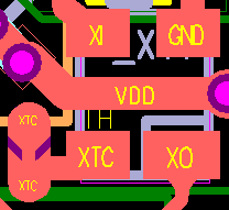
I use a modified 0402 solder jumper ( I 'borrowed' from SiLabs eval designs) that is also just the right size to fit a via-in-pad, so it can squeeze into small spaces, and fit on either or both sides.
They do two paste versions, a paste-one for NC and no-paste-one for NO
Yes, plus Mini-USB 5V cabled supplies are now rare, and the comments admits that mobile chargers are all micro-USB - so that's easy for everyone to find, even if there is 'cable attrition'
Looks nice.
You may need more parallel vias in the high current and thermal paths, especially around the 1v8 switcher ?
I think rogloh added some copper area to 1v8 inductor pad to help cool the inductor on his layout.