

Prop2 Analog Test Chip Arrived!
 cgracey
Posts: 14,323
cgracey
Posts: 14,323
in Propeller 2
We've got 100 of these:
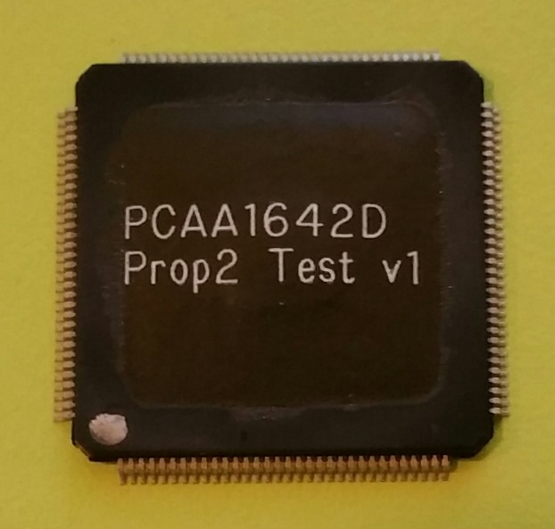
I've been so busy struggling with the ROM code that I haven't made a board for these, yet. I'll make a board that will plug into the Prop123, so that these chips can be exercised as if they were part of the core logic.
I've been so busy struggling with the ROM code that I haven't made a board for these, yet. I'll make a board that will plug into the Prop123, so that these chips can be exercised as if they were part of the core logic.
622 x 593 - 53K
Comments
And here is the pinout, as if it had gone into the originally intended 80-pin package:
Everything. All elements of the pad frame are in there. So, there are two I/O pins (4 fuses in each), the clock pads (RCFAST/RCSLOW/XTAL/PLL), and the RESn and TESn pads.
Good luck with the testing.
Starts biting finger nails, nervously waiting for test results...
Fingers and toes crossed that all functions as expected!!!
You might be able to buy a PLCC128 breakout board off the shelf to start some testing while you layout and wait for your own pcbs.
BTW what is the pitch of these chips?
Looks like it's .5mm. Plenty of breakout boards for that footprint.
Ken Gracey
I had a quick look but didn't find much in square 128 pin 0.5mm. There were rectangular 128 pin qfp package breakouts (RE470), however I suspect the 144 pin breakouts would work as these are also designed for 20x20mm
http://uk.rs-online.com/web/p/surface-mount-smt-to-through-hole-adapter-boards/3675219/
Hey, will we be able to test DAC input?
It has two instances of the I/O pad. So, we've got both DAC and ADC.
Which foundry did you use? I expected to be ON Semi, and on a different package as well. Also, are those 180nm testchips?
Kind regards, Samuel Lourenço
Yes, OnSemi made these and they use the ONC18 process.
Not quite. This is only the ring (analog, smart pins, etc), no cogs or hub memory.
Seems like maybe it could...
Limited Colour VGA and Limited Colour Component Video should be possible with 2 DACs.
The final change-rate will be dictated by how quickly the test interface can update the DACS, so it might not manage full VGA pixel-change-rates.
Could you instead just use two chips to get 4 I/O?
Strictly, yes, but whatever is driving the test chip, I figured could easily manage H,V Syncs.
You could just duplicate/divert the signals to the P2 test silicon and see how it looks, side by side.