@jmg said:
Of course, they are even harder to see on the floor
Yes, and they are a nightmare to hand solder. I have some of those 563 packages on my carrier board and they took me forever to solder.
I can't figure out where this part vanished to but I do hope to find it otherwise I might have to wait for Feb next year to obtain more. I know it was still inside some of its black cut tape so it is not that tiny to see. Right now my bench is a mess anyway and needs a clean up, so hopefully I can hunt it down today.
UPDATE: FOUND IT! It was hidden at the back of my soldering iron station. How it got back there is a mystery.
@evanh said:
Begging for a thermocouple to be sunk into the centre solder blob!
...
I don't think the Prop2 ADCs are anywhere near good enough, not directly anyway.
It's possible but I also wouldn't recommend it. Thermocouples are good for very high or very low temperatures. If you're in the range of typical sensor chips (-20 to +150°C) I'd use something like a TMP102 which is much more convenient. Or if +/-5° tolerance is acceptable a cheap NTC resistor also does the job.
I chose the MCP9701A which is +/- 2C and should do the job and looks to have good sensitivity over the full scale range expected. It also doesn't always need an i2c driver to run in the P2 for temp measurement. Stocks might be getting low so I should order it soon. I do have other i2c devices on the carrier board (LM75A) but these could be read by the supervising micro on it's bus.
Certainly not at this time, the problem is that the existing design needs a switching voltage regulator that can be obtained and this part is fully out of stock until about a year from now at Mouser/Digikey etc thanks to the semiconductor shortages.
If a board was to be made available down the track it would be better to tweak the design to use another regulator with lots of stock and I've not contemplated doing that as yet.
Also I'm not really setup for small scale manufacturing of the boards if doing all the assembly/test myself etc. The tiny quantities just can't justify it and costs/time would be too much.
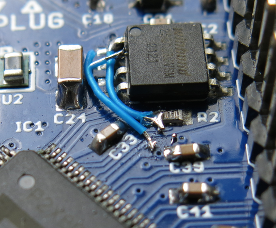
I've hit yet another annoying PCB track break problem with another board I made - these are the 4th and 5th broken tracks I've found over two different boards (P2ME2 & Voyager). For some reason these boards made by the manufacturer keep breaking tracks even though they start out working. I wonder if it is excess pressure on the boards when I connect them together or some other failure. My PCB traces are 6 mil so it is pretty fine. Two PCB tracks to the SPI flash broke sometime in the last few weeks (somewhere under the chip, probably at the join to the SOP-8 pad, given one of them stays on the same layer and has no micro-vias). Strange thing was these were reasonably well protected paths going under the flash chip. I don't see it flexing much there. Maybe next time I'll use 2oz copper. All the broken tracks I've had are underneath devices so it is hard to pinpoint/observe the break, but there is no continuity with the meter when I probe them until I patch them back again.
My wire patch is damn ugly but it seems to fix the issue for now and the P2 on my P2ME2 can now see the SPI flash chip again as it could when the board was first made and I had tested it some weeks back. Thankfully I scraped a via that I could solder to so the connection reaches the P2. There is no way I could hand solder a wire onto the P2 pin.
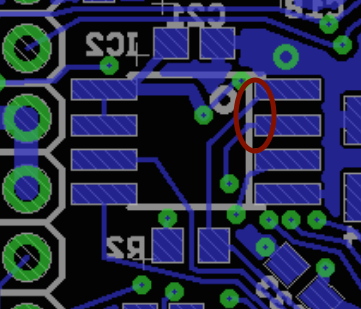
These are the two SPI flash tracks that broke...probably where circled. There was no connection from the flash pad to the via or the pull up resistor they both connected to.
@rogloh said:
.... I wonder if it is excess pressure on the boards when I connect them together or some other failure. My PCB traces are 6 mil so it is pretty fine. Two PCB tracks to the SPI flash broke sometime in the last few weeks (somewhere under the chip, probably at the join to the SOP-8 pad, given one of them stays on the same layer and has no micro-vias). Strange thing was these were reasonably well protected paths going under the flash chip. I don't see it flexing much there. Maybe next time I'll use 2oz copper. All the broken tracks I've had are underneath devices so it is hard to pinpoint/observe the break, but there is no continuity with the meter when I probe them until I patch them back again.
It may be the optics, but the trace by R2, looks much thinner than the trace by IC1 ?
I've used a pin to probe thru solder mask in the past to nail down breaks. See if they are at the step-change in track size ?
I wonder if teardrops would help on the next layout ? I've always favoured those for changes in size.
I also nudge up trace width, to allow for some etching effects so traces are set a little above clearances.
@jmg said:
It may be the optics, but the trace by R2, looks much thinner than the trace by IC1 ?
Here's the original zoomed Eagle image - I checked the track properties and they are 6mil all along those paths.
I wonder if teardrops would help on the next layout ? I've always favoured those for changes in size.
I also nudge up trace width, to allow for some etching effects so traces are set a little above clearances.
@JRoark said:
I use 8 mil as my minimum, even though my vendors specs say they will go smaller. Is this width an option for you?
It might be for another P2ME2 layout perhaps. It could get tricky for the P2 Voyager board though unless I went 4 layers which of course I should do. Routing that parallel LCD group in 8 mil could get harder otherwise.
@Tubular said:
Ok great you got it sorted. Bit of a worry though
Yes, if these breaks keep happening I'll probably never get to finish it! So far at least though there are no design or show stopper problems which has been good, it just appears to be bad soldering/PCB manufacturing or software issues that I'm working through.
@rogloh said:
Yes, if these breaks keep happening I'll probably never get to finish it! So far at least though there are no design or show stopper problems which has been good, it just appears to be bad soldering/PCB manufacturing or software issues that I'm working through.
That's a surprising number of failures tho. I'd try to microscope into exactly where they are happening. Are they all at the large 90' step junctions ?
Maybe the board was just (very) poorly washed before the resist was applied ?
@jmg said:
That's a surprising number of failures tho. I'd try to microscope into exactly where they are happening. Are they all at the large 90' step junctions ?
Maybe the board was just (very) poorly washed before the resist was applied ?
Possibly. I guess for a deal for $5 for 10 boards you can't expect too much.
@jmg said:
Of course, they are even harder to see on the floor
Yes, and they are a nightmare to hand solder. I have some of those 563 packages on my carrier board and they took me forever to solder.
I can't figure out where this part vanished to but I do hope to find it otherwise I might have to wait for Feb next year to obtain more. I know it was still inside some of its black cut tape so it is not that tiny to see. Right now my bench is a mess anyway and needs a clean up, so hopefully I can hunt it down today.
UPDATE: FOUND IT! It was hidden at the back of my soldering iron station. How it got back there is a mystery.
@rogloh said:
These are the two SPI flash tracks that broke...probably where circled. There was no connection from the flash pad to the via or the pull up resistor they both connected to.
Would rounding out those sharp inside angles on the traces to the pads help?
@rogloh said:
These are the two SPI flash tracks that broke...probably where circled. There was no connection from the flash pad to the via or the pull up resistor they both connected to.
Would rounding out those sharp inside angles on the traces to the pads help?
Possibly - but I tend to use 45 degree angles in lots of other places and they seem to be okay. Maybe mitre-ing the tracks would help. Maybe I'd hairline cracked it somehow due to thermal expansion/contraction of the flash chip (which is quite thick) and it then degraded over time with movement or installing into a socket - was working okay at the start but failed soon after.
What does 2oz copper mean? Why oz and not metric?
It's 2oz of copper used per square foot of PCB I think. A lot of PCB stuff is done in imperial measurements while drill holes mainly seem to be in mm. Weirdly mil's are in thousandths of an inch (which is a little bit of metric added on top as well for fun).


Comments
Yes, and they are a nightmare to hand solder. I have some of those 563 packages on my carrier board and they took me forever to solder.
I can't figure out where this part vanished to but I do hope to find it otherwise I might have to wait for Feb next year to obtain more. I know it was still inside some of its black cut tape so it is not that tiny to see. Right now my bench is a mess anyway and needs a clean up, so hopefully I can hunt it down today.
UPDATE: FOUND IT! It was hidden at the back of my soldering iron station. How it got back there is a mystery.
Well, it has legs, even if they are short.")
I'll show myself out ...
Have you seen this?
https://forums.parallax.com/discussion/173508/direct-thermocouple-measurement#p1
Yep, Ariba also linked it. And I do remember it again, having made comments there. I had forgotten about it.
It does solve much. But the noise at high gain is still likely an issue. And I'm not sure how accurate it ever was either.
It's possible but I also wouldn't recommend it. Thermocouples are good for very high or very low temperatures. If you're in the range of typical sensor chips (-20 to +150°C) I'd use something like a TMP102 which is much more convenient. Or if +/-5° tolerance is acceptable a cheap NTC resistor also does the job.
I chose the MCP9701A which is +/- 2C and should do the job and looks to have good sensitivity over the full scale range expected. It also doesn't always need an i2c driver to run in the P2 for temp measurement. Stocks might be getting low so I should order it soon. I do have other i2c devices on the carrier board (LM75A) but these could be read by the supervising micro on it's bus.
Sooo, can the P2ME2 be bought somewhere?
Certainly not at this time, the problem is that the existing design needs a switching voltage regulator that can be obtained and this part is fully out of stock until about a year from now at Mouser/Digikey etc thanks to the semiconductor shortages.
If a board was to be made available down the track it would be better to tweak the design to use another regulator with lots of stock and I've not contemplated doing that as yet.
Also I'm not really setup for small scale manufacturing of the boards if doing all the assembly/test myself etc. The tiny quantities just can't justify it and costs/time would be too much.
I've hit yet another annoying PCB track break problem with another board I made - these are the 4th and 5th broken tracks I've found over two different boards (P2ME2 & Voyager). For some reason these boards made by the manufacturer keep breaking tracks even though they start out working. I wonder if it is excess pressure on the boards when I connect them together or some other failure. My PCB traces are 6 mil so it is pretty fine. Two PCB tracks to the SPI flash broke sometime in the last few weeks (somewhere under the chip, probably at the join to the SOP-8 pad, given one of them stays on the same layer and has no micro-vias). Strange thing was these were reasonably well protected paths going under the flash chip. I don't see it flexing much there. Maybe next time I'll use 2oz copper. All the broken tracks I've had are underneath devices so it is hard to pinpoint/observe the break, but there is no continuity with the meter when I probe them until I patch them back again.
My wire patch is damn ugly but it seems to fix the issue for now and the P2 on my P2ME2 can now see the SPI flash chip again as it could when the board was first made and I had tested it some weeks back. Thankfully I scraped a via that I could solder to so the connection reaches the P2. There is no way I could hand solder a wire onto the P2 pin.
These are the two SPI flash tracks that broke...probably where circled. There was no connection from the flash pad to the via or the pull up resistor they both connected to.
It may be the optics, but the trace by R2, looks much thinner than the trace by IC1 ?
I've used a pin to probe thru solder mask in the past to nail down breaks. See if they are at the step-change in track size ?
I wonder if teardrops would help on the next layout ? I've always favoured those for changes in size.
I also nudge up trace width, to allow for some etching effects so traces are set a little above clearances.
Here's the original zoomed Eagle image - I checked the track properties and they are 6mil all along those paths.
Yeah good idea for next time.
Ok great you got it sorted. Bit of a worry though
I use 8 mil as my minimum, even though my vendors specs say they will go smaller. Is this width an option for you?
It might be for another P2ME2 layout perhaps. It could get tricky for the P2 Voyager board though unless I went 4 layers which of course I should do. Routing that parallel LCD group in 8 mil could get harder otherwise.
Yes, if these breaks keep happening I'll probably never get to finish it! So far at least though there are no design or show stopper problems which has been good, it just appears to be bad soldering/PCB manufacturing or software issues that I'm working through.
That's a surprising number of failures tho. I'd try to microscope into exactly where they are happening. Are they all at the large 90' step junctions ?
Maybe the board was just (very) poorly washed before the resist was applied ?
Possibly. I guess for a deal for $5 for 10 boards you can't expect too much.
Interesting board.
But, Gerbers would be useful ...
lolol
Would rounding out those sharp inside angles on the traces to the pads help?
What does 2oz copper mean? Why oz and not metric?
is that .008 inches?
Possibly - but I tend to use 45 degree angles in lots of other places and they seem to be okay. Maybe mitre-ing the tracks would help. Maybe I'd hairline cracked it somehow due to thermal expansion/contraction of the flash chip (which is quite thick) and it then degraded over time with movement or installing into a socket - was working okay at the start but failed soon after.
It's 2oz of copper used per square foot of PCB I think. A lot of PCB stuff is done in imperial measurements while drill holes mainly seem to be in mm. Weirdly mil's are in thousandths of an inch (which is a little bit of metric added on top as well for fun).
It would be nice is every dimension was just done in metric.
The whole weight thing does seem weird. It's about 35 micron per oz.
Yes. I verbally use the term "thou" so as not to be confusing with the shortened "mill" for millimetre.