Being a signal integrity maniac, the solelly advice I can provide relates to the GND return path, for the trace connecting XI to the crystal/oscillator pin.
Despite the two L-shaped gaps (at GND) are meant to ease the soldering of the bypass cap, they'll also impose some imbalance at this net.
Not any desperate call to 911, but it'll be better to avoid such disturbances, if possible.
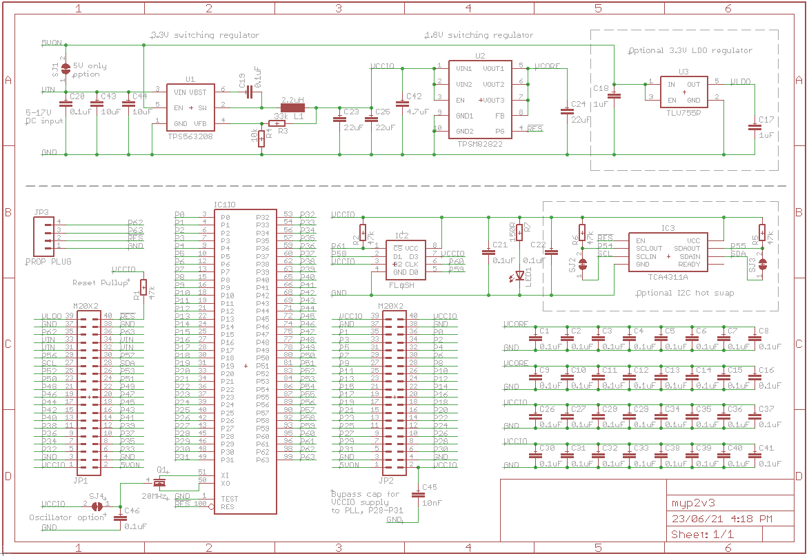
The SMPS still bothers me a little...
The input caps are better on the same side as the SMPS, as they have the worst edges, whilst the output caps have a triangle wave current, so they could go to the bottom, and then the inductor can move further from the Xtal/PLL areas.
ie just swap which caps are top/bottom.
The 3v3 take off should ideally be downstream of the filter caps, not on the inductor side, as any common mode track inductance adds to supply noise.
The 1v8 regulator is cute, but very small, and a source of heat-density - it could move further away from the P2, to allocate it more copper and spread the heat sources apart ?
I was thinking about this heat density too, but at ~91% or better efficiency I don't think its so critical.
If you P2 is consuming 1A then its emitting 1800mW, and the switcher just 180mW out at one edge. Yes it does compound and the switcher will get warmer, but when you factor how much of the power share is being dissipated by the P2 the switcher position seems a little less critical
@Tubular said:
I was thinking about this heat density too, but at ~91% or better efficiency I don't think its so critical.
If you P2 is consuming 1A then its emitting 1800mW, and the switcher just 180mW out at one edge. Yes it does compound and the switcher will get warmer, but when you factor how much of the power share is being dissipated by the P2 the switcher position seems a little less critical
True, but my thinking was the area of that tiny TI switcher is much less than 1/10 th of the P2 large footprint, so it would prefer more cooling-copper, and some more distance from that P2 heat source. Cooler = more reliable.
Being a signal integrity maniac, the solelly advice I can provide relates to the GND return path, for the trace connecting XI to the crystal/oscillator pin.
Despite the two L-shaped gaps (at GND) are meant to ease the soldering of the bypass cap, they'll also impose some imbalance at this net.
Not any desperate call to 911, but it'll be better to avoid such disturbances, if possible.
Hope it helps.
Henrique
Ok not entirely sure if you meant the area without ground near the bypass cap for the oscillator option but I think that part might have changed since... I'll post a picture shortly when I fire up the PCB layout PC and get it.
@rogloh said:
Ok not entirely sure if you meant the area without ground near the bypass cap for the oscillator option but I think that part might have changed since... I'll post a picture shortly when I fire up the PCB layout PC and get it.
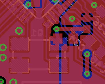
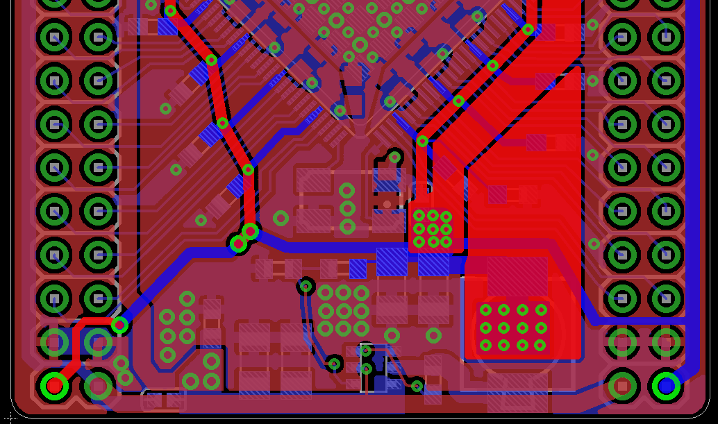
I was talking about the following return path (cropped view):
Xi signal path is crossing over two areas of missing GND continuity, at the other layer.
@jmg said:
The SMPS still bothers me a little...
The input caps are better on the same side as the SMPS, as they have the worst edges, whilst the output caps have a triangle wave current, so they could go to the bottom, and then the inductor can move further from the Xtal/PLL areas.
ie just swap which caps are top/bottom.
I'll look at this. I'm more interested in moving the caps to the bottom for another reason (height), as some bulk caps can be a bit taller than the 0603 bypass caps. E.g. I probably don't really want thicker 2-3mm devices on this surface in my own project carrying 12V power shorting against any metal components situated above it in my enclosure. I still need to measure the exact clearance I have to be sure of what is possible...also depends on header pin height too and the fan space I need.
The 3v3 take off should ideally be downstream of the filter caps, not on the inductor side, as any common mode track inductance adds to supply noise.
Yes this is something that has still been bugging me too, I just didn't want to run a long trace that could couple noise from the power lines nearby. I can't say I've followed all of the recommended layout advice in the data sheet for this part which isn't ideal. The shape of the spare area and the size of the parts isn't helping...
The 1v8 regulator is cute, but very small, and a source of heat-density - it could move further away from the P2, to allocate it more copper and spread the heat sources apart ?
I think I'll probably be leaving this one in its place. It's a bit of a squeeze around there but I'll take a look if it can move away a little. You can see I did try to add lots of vias to help transfer the heat and have since increase the 3.3V copper plane area around it too. Will post another image.
@rogloh said:
Ok not entirely sure if you meant the area without ground near the bypass cap for the oscillator option but I think that part might have changed since... I'll post a picture shortly when I fire up the PCB layout PC and get it.
I was talking about the following return path (cropped view):
Xi signal path is crossing over two areas of missing GND continuity, at the other layer.
:
Ok thanks, yes I see. I think that is fixed now in the updated version but I will double check.
@jmg I was able to move that 1.8V regulator a little further away from the P2 and give more copper to the 1.8V plane.
Later tonight or tomorrow I might look at the 3.3V side to see what is possible. If I move the (slimmer) resistors to the top side and run the feedback trace and VCCIO along the bottom edge of the board but on the top layer it could free some room for caps on the input side to be moved to the other layer....
Also a Mouser delivery just arrived right now too with some of the parts for this stuff and some SRAMs so I need to check that out as well.
@rogloh said:
@jmg I was able to move that 1.8V regulator a little further away from the P2 and give more copper to the 1.8V plane.
That looks good
Another thought is that the series SMPS design will have 1v8 switcher noise load on the 3v3, so a simple split track pi-filter could help.
ie maybe add another bulk cap on the red side, (somewhere near the power on label) and slit the 3v3 plane, so the 1v8 takeoff path avoids the P2 pins entirely. PCB traces then become noise filters.
@jmg, I can look into splitting the 3.3V plane so the connections on the right to all those VCCIO pins are fed by a separate trace but it will stil have to eventually join up to the main 3.3V supply plane, somewhere closer to the crystal. Not sure if another bulk cap at the 1.8V regulator end of the trace will make a huge difference, as there is already one fitted right there underneath it near all those vias feeding the 1.8V regulator from the top layer but I could fit a smaller bypass cap on the top layer between 3.3V and ground to try to filter off the high frequency switching spikes, or at least have some pads to do so if this looks like a problem. I also wonder if it makes sense to feed the VCCIO pin for P28-31 (PLL supply) from 3.3V via a small resistor to make a low pass filter and help clean up the supply even more to this pin. I think Peter had used a similar RC filter path on his own board going to that pin. It wouldn't hurt to feed this pin through a resistor pad which could always be fitted with zero ohms anyway.
If my 3.3V LDO had the current capacity it'd be useful for using it as the 3.3V supply for the P2 VCCIO but it is only rated to 500mA which I don't think is enough current if I'm switching 18bit parallel video output and supplying SD and Ethernet components as well - I'm really just using the optional LDO to power some 24bit audio DAC stuff off board which I want to stay relatively clean from switching noise. It doesn't actually get used on this P2 board. A switching regulator is still going to be more efficient and the bonus is that the one I've used can be fed up to 17V which keeps the input current lower. My system can be fed by ~6-14.2VDC depending on power source, eg. 2xLi-Ion or a 12V adapter/car.
@rogloh said:
Here's a split 3.3V, is this what you meant @jmg? There is an extra bypass cap up near all the vias too now, C47.
Yes, tho I'd have placed C47 nearer the power on label where its gnd path to the other GND pins of the SMPS is shorter & fatter.
The 3v3 take off is still under the L ? Whilst that allows more vias, it loses the low pass nature of the L-C-C, so to me, a better take off is above the right hand C25.
Ceramic caps can have single-digit nH self inductance, so the 'ideal' PCB routing is like the RF-Feedthrus, where a 'noisy' trace comes in one side and the 'clean' trace comes out the other side.
I can easily move C47 about. Yeah I've not started on the 3.3V changes at the lower edge of the board but I'll look at this next. I'll also try to do the feedback path nearer the caps, and I could possibly take the power out at that end and split the copper near the inductor. I do want those vias under the inductor, in my last carrier board design I didn't have nearly enough copper there to transfer the heat away and the heat really built up - though this inductor is larger now this time around and much lower resistance which also helps.
@rogloh said:
I do want those vias under the inductor, in my last carrier board design I didn't have nearly enough copper there to transfer the heat away and the heat really built up - though this inductor is larger now this time around and much lower resistance which also helps.
That makes sense, so maybe 3 zones ? - an Inductor-cooling area, a P2 3v3 strip, and a 1v8 SMPS path, for the noisy currents to take.
Oh, I wouldn't recommend having a 3V3 switcher at all. Supply the 1V8 switcher from the 5 Volts and just have an LDO for 3V3. Which is what Parallax have ended up with in all their recent designs. Is there some reason for the VIOs to be high current?
No, it's mainly the fact that I now need to feed in 12V instead of 5V as VIN (to save my 5V regulator inductor elsewhere on the carrier board from frying) and the 1.8V switcher is limited to accepting 5.5V, so I drop down to 3.3V first, as that regulator allows up to 17V.
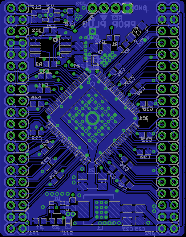
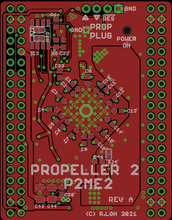
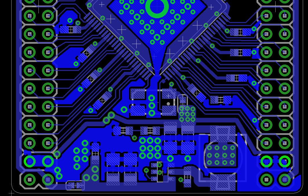
@jmg, I've moved the 3.3V stuff about and was able to get the caps on the bottom layer and adhere to more of the guidelines and move the inductor further away too. The only concern is that I had to bring a portion of the switching path up to the top layer over the input caps. Hopefully this doesn't couple too much noise to the ground. You can see through the top red layer to the layer under it where the components are fitted now. I split the 3.3V into three zones coming of the bulk output caps (power to 1.8V, thermal portion above inductor, and power to VCCIO and other header pin outputs). Still have to route a couple of nets.
Update: Actually looking at it now, I might be able to swap the positions of the input caps and SOT package to remedy that switching path issue...
I believe you could also elongate that track a little bit to the right, in order to provide space for at least an extra via, communicating both layers, without sacrificing too much the GND area.
I was able to rework the layout again with that last idea I mentioned and I think it's good to go now. It's a much tighter loop now and all regulator components are on the same side as the P2. Ground is fully routed through on both layers too and surrounds the sensitive areas. Hopefully this board can go out this week.
@rogloh said:
I was able to rework the layout again with that last idea I mentioned and I think it's good to go now. It's a much tighter loop now and all regulator components are on the same side as the P2.
Looking good could the bootstrap cap flip to the other side to tighten smps and allow more copper around switcher ?
Is there routing room to then slip c20, or c43?, into that free space ?
Yeah makes good sense jmg, it's just a minor tweak and the boost cap is slim like the other bypass caps on that layer.
Have wrapped up my board now with final jmg suggestion, and plan to submit this one via Tubular tomorrow to get made.
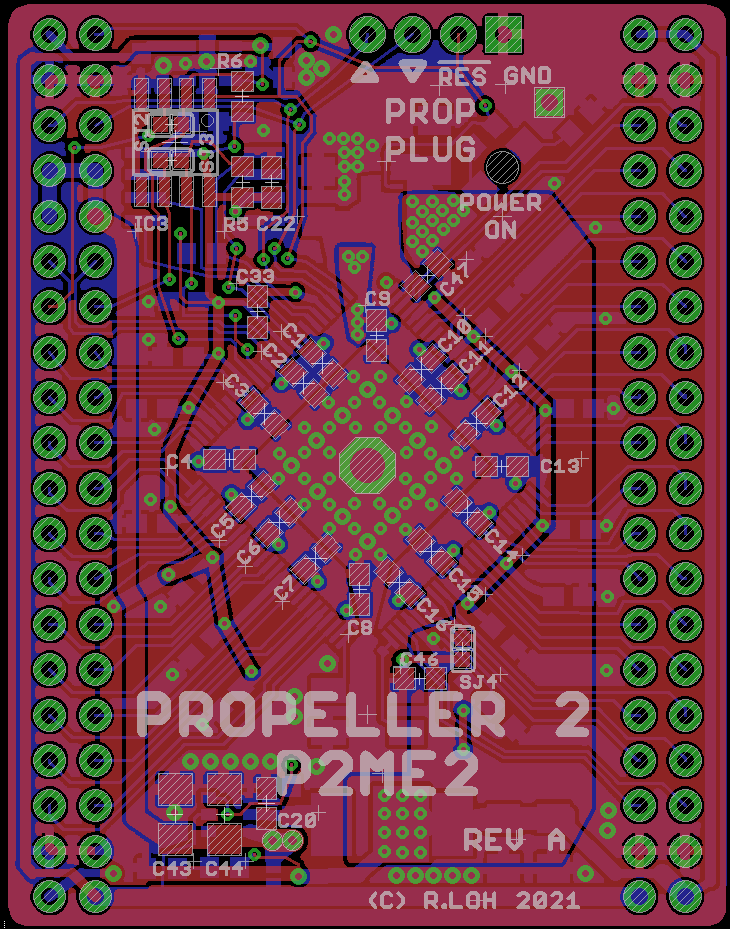
In a remaining bit of space I also added in an optional temperature sensor near the P2 that can drive analog out to P16 via a resistor so the pin can still be used for other output purposes. I am planning to get the stencil for the bottom layer so the whole bottom layer could be done in an oven, but apart from that tiny 1.8V regulator module, in theory this board is hand solderable if you can handle the 0.5mm P2 pitch and 0603 components. It looks straightforward enough to get a soldering iron around these components on the top layer from what I see in the images below.


Comments
Hi @rogloh,
Being a signal integrity maniac, the solelly advice I can provide relates to the GND return path, for the trace connecting XI to the crystal/oscillator pin.
Despite the two L-shaped gaps (at GND) are meant to ease the soldering of the bypass cap, they'll also impose some imbalance at this net.
Not any desperate call to 911, but it'll be better to avoid such disturbances, if possible.
Hope it helps.
Henrique
The SMPS still bothers me a little...
The input caps are better on the same side as the SMPS, as they have the worst edges, whilst the output caps have a triangle wave current, so they could go to the bottom, and then the inductor can move further from the Xtal/PLL areas.
ie just swap which caps are top/bottom.
The 3v3 take off should ideally be downstream of the filter caps, not on the inductor side, as any common mode track inductance adds to supply noise.
The 1v8 regulator is cute, but very small, and a source of heat-density - it could move further away from the P2, to allocate it more copper and spread the heat sources apart ?
I was thinking about this heat density too, but at ~91% or better efficiency I don't think its so critical.
If you P2 is consuming 1A then its emitting 1800mW, and the switcher just 180mW out at one edge. Yes it does compound and the switcher will get warmer, but when you factor how much of the power share is being dissipated by the P2 the switcher position seems a little less critical
True, but my thinking was the area of that tiny TI switcher is much less than 1/10 th of the P2 large footprint, so it would prefer more cooling-copper, and some more distance from that P2 heat source. Cooler = more reliable.
Ok not entirely sure if you meant the area without ground near the bypass cap for the oscillator option but I think that part might have changed since... I'll post a picture shortly when I fire up the PCB layout PC and get it.
I was talking about the following return path (cropped view):
Xi signal path is crossing over two areas of missing GND continuity, at the other layer.
:
I'll look at this. I'm more interested in moving the caps to the bottom for another reason (height), as some bulk caps can be a bit taller than the 0603 bypass caps. E.g. I probably don't really want thicker 2-3mm devices on this surface in my own project carrying 12V power shorting against any metal components situated above it in my enclosure. I still need to measure the exact clearance I have to be sure of what is possible...also depends on header pin height too and the fan space I need.
Yes this is something that has still been bugging me too, I just didn't want to run a long trace that could couple noise from the power lines nearby. I can't say I've followed all of the recommended layout advice in the data sheet for this part which isn't ideal. The shape of the spare area and the size of the parts isn't helping...
I think I'll probably be leaving this one in its place. It's a bit of a squeeze around there but I'll take a look if it can move away a little. You can see I did try to add lots of vias to help transfer the heat and have since increase the 3.3V copper plane area around it too. Will post another image.
Ok thanks, yes I see. I think that is fixed now in the updated version but I will double check.
Here's the latest stuff.
Here's the crystal stuff @Yanomani, XO trace is fully covered.
My internet connection got stuck, for a while... Working now, but who knows for how long it will last...
Sorry for the confusion between XI/XO; I was looking from the wrong perspective.
Now it seems to be right!
@jmg I was able to move that 1.8V regulator a little further away from the P2 and give more copper to the 1.8V plane.
Later tonight or tomorrow I might look at the 3.3V side to see what is possible. If I move the (slimmer) resistors to the top side and run the feedback trace and VCCIO along the bottom edge of the board but on the top layer it could free some room for caps on the input side to be moved to the other layer....
Also a Mouser delivery just arrived right now too with some of the parts for this stuff and some SRAMs so I need to check that out as well.
That looks good")
Another thought is that the series SMPS design will have 1v8 switcher noise load on the 3v3, so a simple split track pi-filter could help.
ie maybe add another bulk cap on the red side, (somewhere near the power on label) and slit the 3v3 plane, so the 1v8 takeoff path avoids the P2 pins entirely. PCB traces then become noise filters.
@jmg, I can look into splitting the 3.3V plane so the connections on the right to all those VCCIO pins are fed by a separate trace but it will stil have to eventually join up to the main 3.3V supply plane, somewhere closer to the crystal. Not sure if another bulk cap at the 1.8V regulator end of the trace will make a huge difference, as there is already one fitted right there underneath it near all those vias feeding the 1.8V regulator from the top layer but I could fit a smaller bypass cap on the top layer between 3.3V and ground to try to filter off the high frequency switching spikes, or at least have some pads to do so if this looks like a problem. I also wonder if it makes sense to feed the VCCIO pin for P28-31 (PLL supply) from 3.3V via a small resistor to make a low pass filter and help clean up the supply even more to this pin. I think Peter had used a similar RC filter path on his own board going to that pin. It wouldn't hurt to feed this pin through a resistor pad which could always be fitted with zero ohms anyway.
If my 3.3V LDO had the current capacity it'd be useful for using it as the 3.3V supply for the P2 VCCIO but it is only rated to 500mA which I don't think is enough current if I'm switching 18bit parallel video output and supplying SD and Ethernet components as well - I'm really just using the optional LDO to power some 24bit audio DAC stuff off board which I want to stay relatively clean from switching noise. It doesn't actually get used on this P2 board. A switching regulator is still going to be more efficient and the bonus is that the one I've used can be fed up to 17V which keeps the input current lower. My system can be fed by ~6-14.2VDC depending on power source, eg. 2xLi-Ion or a 12V adapter/car.
Here's a split 3.3V, is this what you meant @jmg? There is an extra bypass cap up near all the vias too now, C47.
Yes, tho I'd have placed C47 nearer the power on label where its gnd path to the other GND pins of the SMPS is shorter & fatter.
The 3v3 take off is still under the L ? Whilst that allows more vias, it loses the low pass nature of the L-C-C, so to me, a better take off is above the right hand C25.
Ceramic caps can have single-digit nH self inductance, so the 'ideal' PCB routing is like the RF-Feedthrus, where a 'noisy' trace comes in one side and the 'clean' trace comes out the other side.
I can easily move C47 about. Yeah I've not started on the 3.3V changes at the lower edge of the board but I'll look at this next. I'll also try to do the feedback path nearer the caps, and I could possibly take the power out at that end and split the copper near the inductor. I do want those vias under the inductor, in my last carrier board design I didn't have nearly enough copper there to transfer the heat away and the heat really built up - though this inductor is larger now this time around and much lower resistance which also helps.
That makes sense, so maybe 3 zones ? - an Inductor-cooling area, a P2 3v3 strip, and a 1v8 SMPS path, for the noisy currents to take.
Yeah that's what I'm thinking at this point.
I could make the cooling area bigger but didn't want to put 3.3V over the crystal.
Oh, I wouldn't recommend having a 3V3 switcher at all. Supply the 1V8 switcher from the 5 Volts and just have an LDO for 3V3. Which is what Parallax have ended up with in all their recent designs. Is there some reason for the VIOs to be high current?
No, it's mainly the fact that I now need to feed in 12V instead of 5V as VIN (to save my 5V regulator inductor elsewhere on the carrier board from frying) and the 1.8V switcher is limited to accepting 5.5V, so I drop down to 3.3V first, as that regulator allows up to 17V.
Okay, right. I've not been following, just happened to look at the schematic.
@jmg, I've moved the 3.3V stuff about and was able to get the caps on the bottom layer and adhere to more of the guidelines and move the inductor further away too. The only concern is that I had to bring a portion of the switching path up to the top layer over the input caps. Hopefully this doesn't couple too much noise to the ground. You can see through the top red layer to the layer under it where the components are fitted now. I split the 3.3V into three zones coming of the bulk output caps (power to 1.8V, thermal portion above inductor, and power to VCCIO and other header pin outputs). Still have to route a couple of nets.
Update: Actually looking at it now, I might be able to swap the positions of the input caps and SOT package to remedy that switching path issue...
Hi rogloh
I believe you could also elongate that track a little bit to the right, in order to provide space for at least an extra via, communicating both layers, without sacrificing too much the GND area.
Yes, I should do that. This path feeds current for multiple sinks.
I was able to rework the layout again with that last idea I mentioned and I think it's good to go now. It's a much tighter loop now and all regulator components are on the same side as the P2. Ground is fully routed through on both layers too and surrounds the sensitive areas. Hopefully this board can go out this week.
looks good
Enjoy!
Mike
Looking good") could the bootstrap cap flip to the other side to tighten smps and allow more copper around switcher ?
could the bootstrap cap flip to the other side to tighten smps and allow more copper around switcher ?
Is there routing room to then slip c20, or c43?, into that free space ?
Cheers Mike!
Yeah makes good sense jmg, it's just a minor tweak and the boost cap is slim like the other bypass caps on that layer.
Have wrapped up my board now with final jmg suggestion, and plan to submit this one via Tubular tomorrow to get made.
In a remaining bit of space I also added in an optional temperature sensor near the P2 that can drive analog out to P16 via a resistor so the pin can still be used for other output purposes. I am planning to get the stencil for the bottom layer so the whole bottom layer could be done in an oven, but apart from that tiny 1.8V regulator module, in theory this board is hand solderable if you can handle the 0.5mm P2 pitch and 0603 components. It looks straightforward enough to get a soldering iron around these components on the top layer from what I see in the images below.
Looks good, I'll finish up my stuff during the day tomorrow and we can hit 'send'