@Yanomani said:
The ~2.5 Ohm reading is not any good, you should be having a bad contact somewhere else, including the exposed pad.
Yeah I'm worried about that. The corner tip to corner tip resistance read the same as touching the probes directly, but going through to the exposed pad added about 2.5 ohms more. At one point it also seemed to increase its resistance again as the device cooled before I remelted again and it lowered again.
Did you spreaded at least some kind of a layer of fresh solder paste at any of the pcb land pattern, or the exposed pad, before seating the package onto the pbc?
I really agonized over putting on some paste there before placement and hand soldering but was concerned about shorts underneath or it raising the chip up too high to solder reliably so in the end decided against it and hoped I could get enough solder to go down into the hole. I did add flux in there beforehand too but perhaps that has formed some type of thin barrier layer that messed up the grounding connection.
Addit: doesn't you have any no clean solder flux for reflow, compatible with the solder paste you're using (perhaps Kester 951 (lead free), Kester 186 (rosin) or other good similar)?
It's a water based flux that I used. Kester 2331-ZX. If I melt it long enough it might just boil off but I just don't want to overheat the chip.
EDIT: I just reheated the GND hole solder and saw some flux bubbling up through the vias and now I do have continuity to GND from those corner spots.
Hi rogloh, please, watch out carefully; this "bubbling up" are a sure sign of outgassing, and can carry/expell micro solder bumps very far from the area where they're blowing.
Like micro volcanos, the "bubbling" can also be occuring near the pin frame area, leaving solder bumps, or even filaments (whiskers), really hard to notice, without excellent illumination and loupes/microscopes.
Please do yourself a favour and don't mess with water based flux. It is meant for high volume production to save a few cent per kg of solder paste and to allow for solvent free washing. Washing in turn requires careful drying. A single droplet of water trapped under the chip will ruin everything.
This is all not needed for manual soldering and rework. You should use no-clean flux. This requires no washing at all and is much less corrosive and less sensitive to long storage. And don't try to dilute old and dryed out paste with alcohol or solvents. If it's leaded solder it might work if you add some liquid flux and stirr well. If it's lead free it won't. Throw it away and buy new one.
The correct stencil pattern for the P2 exposed pad should be something like this:
Only 1/3 to 1/2 of the area of the GND pad should be open for paste printing. If you apply too much without channels for the vapours to escape then the paste blob will boil and the package will swim on it so thet the gull wing pins will loose contact to their pads.
@rogloh said:
Only thing I don't like is that I measured ~2.5 ohms via this path. Is that to be expected or is my GND a bad connection?
You should be able to compare measurements with a reflow board, to check it is right ballpark.
Another path is to use the clamp diodes on IO, if you pick say 8 io and reverse feed ~100mA into that path, the diode drops should be identical to a good board.
If you wire unknown + good in series for that test, they have the same current and thermal time.
@ManAtWork said:
Please do yourself a favour and don't mess with water based flux.
This is all not needed for manual soldering and rework. You should use no-clean flux. This requires no washing at all and is much less corrosive and less sensitive to long storage. And don't try to dilute old and dryed out paste with alcohol or solvents. If it's leaded solder it might work if you add some liquid flux and stirr well. If it's lead free it won't. Throw it away and buy new one.
Only 1/3 to 1/2 of the area of the GND pad should be open for paste printing. If you apply too much without channels for the vapours to escape then the paste blob will boil and the package will swim on it so thet the gull wing pins will loose contact to their pads.
I surelly agree with you (my edits to the full quoted version where meant only to spare some space).
@rogloh (and also to any other eventual interested ones); just pick a beer, coffee, tea, wathever seems better, and relax a little, in order to be able to enjoy the following presentation (credits to Indium Corp.):
Up to almost every concern about soldering the exposed pad, QFN and QFP are equivalent concepts...
@ManAtWork said:
Please do yourself a favour and don't mess with water based flux. It is meant for high volume production to save a few cent per kg of solder paste and to allow for solvent free washing. Washing in turn requires careful drying. A single droplet of water trapped under the chip will ruin everything.
Yeah that is a big concern. It might be water trapped under there. I'm going to reheat and hope for improvement.
This is all not needed for manual soldering and rework. You should use no-clean flux. This requires no washing at all and is much less corrosive and less sensitive to long storage. And don't try to dilute old and dryed out paste with alcohol or solvents. If it's leaded solder it might work if you add some liquid flux and stirr well. If it's lead free it won't. Throw it away and buy new one.
Good to know. I'll try to get some no-clean flux in my future orders. So far I haven't diluted any paste I've used. It was still very moist and seemed okay but it was out of date (despite being unopened and refrigerated the whole time). Also I've avoided lead free solder too. No RoHS for me right now.
The correct stencil pattern for the P2 exposed pad should be something like this:
Only 1/3 to 1/2 of the area of the GND pad should be open for paste printing. If you apply too much without channels for the vapours to escape then the paste blob will boil and the package will swim on it so thet the gull wing pins will loose contact to their pads.
Yes, I had read about this too and planned for it by using a very similar land pattern in the stencil with a mix of some larger vias (for venting) and microvias (for good heat transfer) in the gaps between the solder paste squares. Hopefully that will help it enough.
@jmg said:
You should be able to compare measurements with a reflow board, to check it is right ballpark.
Yes good idea. I'll check with the P2-EVAL if I can probe those same points.
Another path is to use the clamp diodes on IO, if you pick say 8 io and reverse feed ~100mA into that path, the diode drops should be identical to a good board.
100mA seems like a lot, unless you mean to distribute this over all 8 IO at once?
@Yanomani said:
@rogloh (and also to any other eventual interested ones); just pick a beer, coffee, tea, wathever seems better, and relax a little, in order to be able to enjoy the following presentation (credits to Indium Corp.):
Another path is to use the clamp diodes on IO, if you pick say 8 io and reverse feed ~100mA into that path, the diode drops should be identical to a good board.
100mA seems like a lot, unless you mean to distribute this over all 8 IO at once?
Yes, all pins at once, sorry was unclear, that's why I said 8 pins, to get a good test current, but easy on each pin.
@evanh said:
Larger diameter vias will always transfer more heat for a given pitch. They have more metal. The limit is mechanical board strength.
Up to a point...
You also need to consider horizontal heat flow on the copper planes, and so vias should not subtract from the ground plane too much.
( I see P2D2 used a 7x7 via array & P2 Eval uses 9x9 array )
Good point, when relying only on the PCB for dissipation, I guess then the plane-to-hole ratio should be graduated from inner vias to outer vias. With inner being more hole and outer being more plane.
Just measured the P2 resistance from its corner tip to GND EP on a P2-EVAL and it was ~0.4 ohms (basically my crummy probe lead's resistance). Resoldered the small GND hole on my P2ME2 at a higher 320C temp for a while, ~ 5-8 secs, and let it melt in a bit more. Seeing the same lower resistance now instead of 2.5 ohms I had yesterday, so fingers crossed that it is fixed now, but time will tell how good this is. I think the best result will probably come with the solder paste when I do the fully loaded 3rd board as long as its 1.8V regulator succeeds. I can probably fix any other connection failures manually I'd expect.
@evanh said:
Larger diameter vias will always transfer more heat for a given pitch. They have more metal. The limit is mechanical board strength.
Up to a point...
You also need to consider horizontal heat flow on the copper planes, and so vias should not subtract from the ground plane too much.
( I see P2D2 used a 7x7 via array & P2 Eval uses 9x9 array )
Good point, when relying only on the PCB for dissipation, I guess then the plane-to-hole ratio should be graduated from inner vias to outer vias. With inner being more hole and outer being more plane.
I hope I have enough via holes for heat transfer. I think my array is only 49 total vias being a mix of some larger venting vias and some microvias plus the large hole in the middle too. Same count as P2D2 anyway. I did read something that indicated once you exceed some number of vias it becomes a diminishing return on heat transfer when I briefly looked at that. Will try to find that link....
EDIT: I think it was this: https://www.pcb-investigator.com/en/blog/thermal-vias-benefits-and-limitations
Sure, I can be wrong, but, what the article is really showing, is the fact that the temperature difference between the top and bottom layers tends to some flat minimum value; even if more vias are added, there is no further relevant gains. Beyound that limit, some other means of removing the excess heat from the affected area needs to be used, which, in fact, is the expected behaviour.
Is like soaking a sponge in water flow: above a certain limit, it stops absorbing liquid, and, the excess will flow out, freely, due to gravity.
In case of excess heat, the "gravity pump" is usually air flow, either natural convection, or forced.
P.S. fortunatelly, you'll never find yourself in need of using something like this:
That makes sense too. The PCB is only a certain size, the air interface limits the dissipation. I'd been thinking about having an attached added heat-sink on the rear originally. And was also thinking of no resist on the back under the prop2 as well.
@rogloh said:
I hope I have enough via holes for heat transfer. I think my array is only 49 total vias being a mix of some larger venting vias and some microvias plus the large hole in the middle too. Same count as P2D2 anyway. I did read something that indicated once you exceed some number of vias it becomes a diminishing return on heat transfer when I briefly looked at that. Will try to find that link....
EDIT: I think it was this: https://www.pcb-investigator.com/en/blog/thermal-vias-benefits-and-limitations
Interesting, I guess that was 1.6mm and 1oz copper ?
That indicates 15 holes is certainly light, which everyone would expect, but even 45 holes has 4.9°C vertical drop on 2 layer board
@jmg , yeah probably the P2-EVAL thermal via count is about right, but hopefully 49 will still do a reasonable job. We'll soon see.
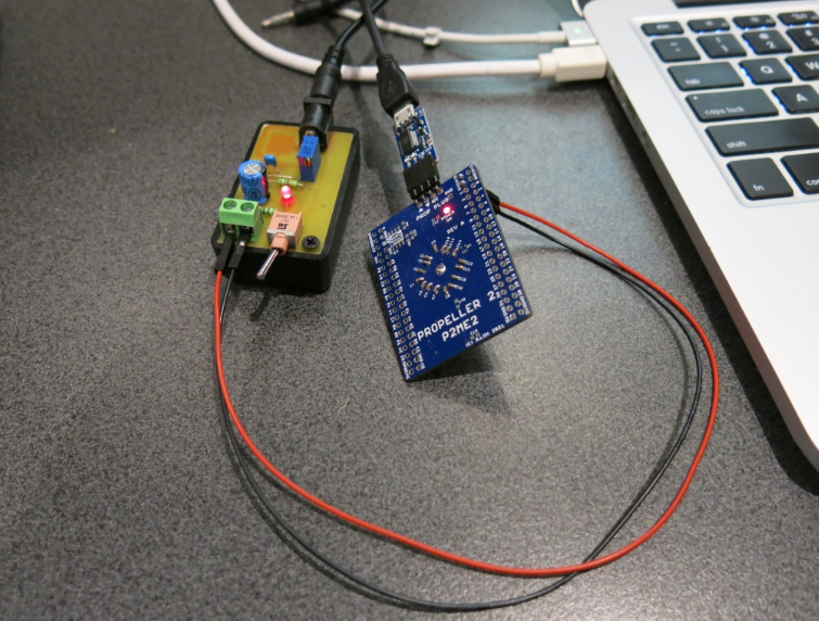
Now can the P2 boot up and be tested without a crystal installed? I've just hand soldered 32 0603 bypass caps (not a pleasant experience) with no shorts and no opens when I buzzed them all out and think there are probably almost enough components on the board to try it out now with a 3.3V supply. I can fit the crystal or oscillator later if this works.
@evanh said:
No need for more without somewhere further for the heat to go.
Yeah that's probably right. This two layer board is already pushing its luck really. I'll like to see how hot it gets. Maybe it will push me to 4 layers when I find out.
@rogloh said:
Now can the P2 boot up and be tested without a crystal installed?
Yes, initial loader is RCFAST only. You can then autobaud, and pop into forth.
My notes say :
Autobaud '> ', Enter TAQOZ from reset + (esc), ie $3E,$20,$1B, then pause >195ms(115200) for TAQOZ to load, then commands are accepted
Lol, yeah there is a certain rotary shape seen there. Was unintentional though.
@jmg said:
@rogloh said:
Now can the P2 boot up and be tested without a crystal installed?
Yes, initial loader is RCFAST only. You can then autobaud, and pop into forth.
My notes say :
Autobaud '> ', Enter TAQOZ from reset + (esc), ie $3E,$20,$1B, then pause >195ms(115200) for TAQOZ to load, then commands are accepted
For loadp2, use the -SINGLE option to ensure it stays in RCFAST during file loading.
Pnut/Proptool both use RCFAST unless using debug, then, I think, they set up the Crystal+PLL.
@JRoark said:
The sweet smell of success! Congrats!
Cheers, and it's only taken me two and a half months to get here. LOL. I thought it would only be about a month or so. Lots of delays with various things holding me up.
.io --- Display the state of all 64 I/O, l=input low, h=input high, L=output low, H=output high
lsio --- Display the condition of all 64 I/O as .io but also display pull-up/down or floats

TAQOZ# lsio ---
P:0000000000111111111122222222223333333333444444444455555555556666
P:0123456789012345678901234567890123456789012345678901234567890123
?:lllllhhhhhhhhhhhhhhhhhhhhhhhhhhhhhlhhhhhhhhhhhhhhhhhhhhhhhhLLLHL
=:ddddd~~~~~~~~~~~~~~~~~~~~~~~~~~~u~?~~~~~~~~~~~~~~~~~~~~~uu~~uu ok


Comments
Yeah I'm worried about that. The corner tip to corner tip resistance read the same as touching the probes directly, but going through to the exposed pad added about 2.5 ohms more. At one point it also seemed to increase its resistance again as the device cooled before I remelted again and it lowered again.
I really agonized over putting on some paste there before placement and hand soldering but was concerned about shorts underneath or it raising the chip up too high to solder reliably so in the end decided against it and hoped I could get enough solder to go down into the hole. I did add flux in there beforehand too but perhaps that has formed some type of thin barrier layer that messed up the grounding connection.
It's a water based flux that I used. Kester 2331-ZX. If I melt it long enough it might just boil off but I just don't want to overheat the chip.
Hi rogloh, please, watch out carefully; this "bubbling up" are a sure sign of outgassing, and can carry/expell micro solder bumps very far from the area where they're blowing.
Like micro volcanos, the "bubbling" can also be occuring near the pin frame area, leaving solder bumps, or even filaments (whiskers), really hard to notice, without excellent illumination and loupes/microscopes.
Please do yourself a favour and don't mess with water based flux. It is meant for high volume production to save a few cent per kg of solder paste and to allow for solvent free washing. Washing in turn requires careful drying. A single droplet of water trapped under the chip will ruin everything.
This is all not needed for manual soldering and rework. You should use no-clean flux. This requires no washing at all and is much less corrosive and less sensitive to long storage. And don't try to dilute old and dryed out paste with alcohol or solvents. If it's leaded solder it might work if you add some liquid flux and stirr well. If it's lead free it won't. Throw it away and buy new one.
The correct stencil pattern for the P2 exposed pad should be something like this:
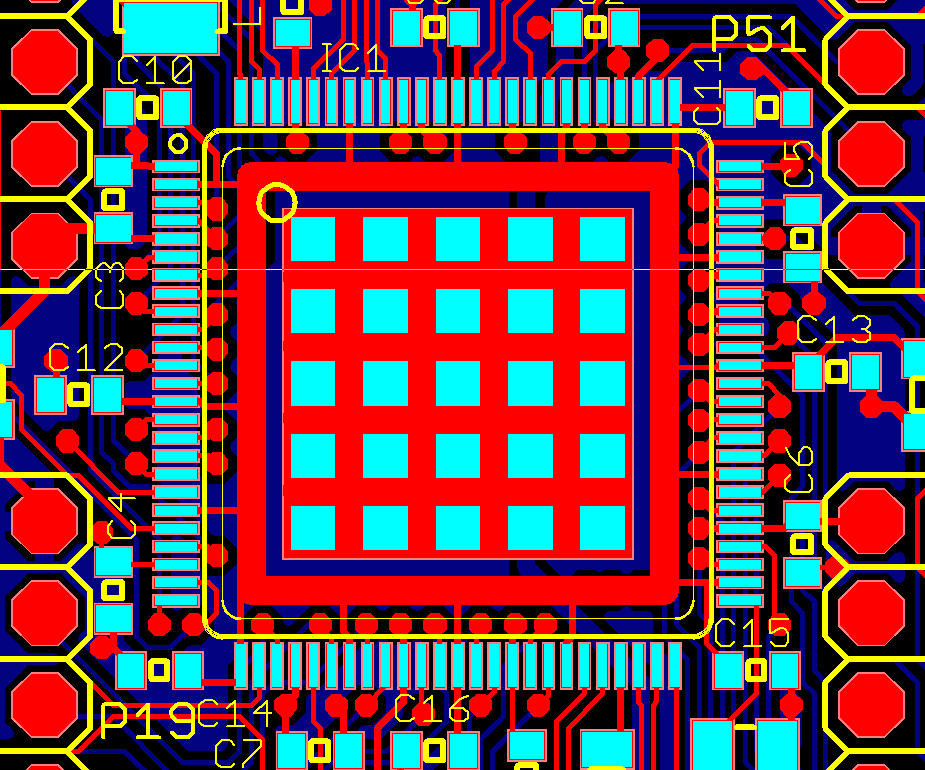
Only 1/3 to 1/2 of the area of the GND pad should be open for paste printing. If you apply too much without channels for the vapours to escape then the paste blob will boil and the package will swim on it so thet the gull wing pins will loose contact to their pads.
You should be able to compare measurements with a reflow board, to check it is right ballpark.
Another path is to use the clamp diodes on IO, if you pick say 8 io and reverse feed ~100mA into that path, the diode drops should be identical to a good board.
If you wire unknown + good in series for that test, they have the same current and thermal time.
I surelly agree with you (my edits to the full quoted version where meant only to spare some space).
@rogloh (and also to any other eventual interested ones); just pick a beer, coffee, tea, wathever seems better, and relax a little, in order to be able to enjoy the following presentation (credits to Indium Corp.):
Up to almost every concern about soldering the exposed pad, QFN and QFP are equivalent concepts...
https://youtube.com/watch?v=_rBYt9rz7y0
Yeah that is a big concern. It might be water trapped under there. I'm going to reheat and hope for improvement.
Good to know. I'll try to get some no-clean flux in my future orders. So far I haven't diluted any paste I've used. It was still very moist and seemed okay but it was out of date (despite being unopened and refrigerated the whole time). Also I've avoided lead free solder too. No RoHS for me right now.
Yes, I had read about this too and planned for it by using a very similar land pattern in the stencil with a mix of some larger vias (for venting) and microvias (for good heat transfer) in the gaps between the solder paste squares. Hopefully that will help it enough.
Yes good idea. I'll check with the P2-EVAL if I can probe those same points.
100mA seems like a lot, unless you mean to distribute this over all 8 IO at once?
Thanks, I will have a look at this.
Larger diameter vias will always transfer more heat for a given pitch. They have more metal. The limit is mechanical board strength.
Yes, all pins at once, sorry was unclear, that's why I said 8 pins, to get a good test current, but easy on each pin.
Up to a point...
You also need to consider horizontal heat flow on the copper planes, and so vias should not subtract from the ground plane too much.
( I see P2D2 used a 7x7 via array & P2 Eval uses 9x9 array )
Good point, when relying only on the PCB for dissipation, I guess then the plane-to-hole ratio should be graduated from inner vias to outer vias. With inner being more hole and outer being more plane.
Just measured the P2 resistance from its corner tip to GND EP on a P2-EVAL and it was ~0.4 ohms (basically my crummy probe lead's resistance). Resoldered the small GND hole on my P2ME2 at a higher 320C temp for a while, ~ 5-8 secs, and let it melt in a bit more. Seeing the same lower resistance now instead of 2.5 ohms I had yesterday, so fingers crossed that it is fixed now, but time will tell how good this is. I think the best result will probably come with the solder paste when I do the fully loaded 3rd board as long as its 1.8V regulator succeeds. I can probably fix any other connection failures manually I'd expect.
I hope I have enough via holes for heat transfer. I think my array is only 49 total vias being a mix of some larger venting vias and some microvias plus the large hole in the middle too. Same count as P2D2 anyway. I did read something that indicated once you exceed some number of vias it becomes a diminishing return on heat transfer when I briefly looked at that. Will try to find that link....
EDIT: I think it was this:
https://www.pcb-investigator.com/en/blog/thermal-vias-benefits-and-limitations
Sure, I can be wrong, but, what the article is really showing, is the fact that the temperature difference between the top and bottom layers tends to some flat minimum value; even if more vias are added, there is no further relevant gains. Beyound that limit, some other means of removing the excess heat from the affected area needs to be used, which, in fact, is the expected behaviour.
Is like soaking a sponge in water flow: above a certain limit, it stops absorbing liquid, and, the excess will flow out, freely, due to gravity.
In case of excess heat, the "gravity pump" is usually air flow, either natural convection, or forced.
P.S. fortunatelly, you'll never find yourself in need of using something like this:
https://led-professional.com/resources-1/articles/reliable-thermal-management-of-high-power-leds-by-haeusermann
Frying-eggs, à la Prop! Non, jamais!
That makes sense too. The PCB is only a certain size, the air interface limits the dissipation. I'd been thinking about having an attached added heat-sink on the rear originally. And was also thinking of no resist on the back under the prop2 as well.
Interesting, I guess that was 1.6mm and 1oz copper ?
That indicates 15 holes is certainly light, which everyone would expect, but even 45 holes has 4.9°C vertical drop on 2 layer board
15 holes ~ 12.9°C
45 holes ~ 4.9°C
170 holes ~ 0.9°C
680 holes ~0.2°C
@jmg , yeah probably the P2-EVAL thermal via count is about right, but hopefully 49 will still do a reasonable job. We'll soon see.
Now can the P2 boot up and be tested without a crystal installed? I've just hand soldered 32 0603 bypass caps (not a pleasant experience) with no shorts and no opens when I buzzed them all out and think there are probably almost enough components on the board to try it out now with a 3.3V supply. I can fit the crystal or oscillator later if this works.
No need for more without somewhere further for the heat to go.
Yeah that's probably right. This two layer board is already pushing its luck really. I'll like to see how hot it gets. Maybe it will push me to 4 layers when I find out.
If there are no electrical gaps or shorts you should be able to, as it boots in RCFAST.
It's a neaty board, indeed!
The bottom side closelly resembles some impossible reincarnation of a Gnome Monosoupape engine.
aviation-history.com/engines/rotary-theory.htm
Though I'm not yet absolutely sure, perhaps you'll be able to even achieve a reasonable DVI video output too, without any crystal installed.
If it's entirely possible, it'll be a world's first!
Fingers crossed here!
Yes, initial loader is RCFAST only. You can then autobaud, and pop into forth.
My notes say :
Autobaud '> ', Enter TAQOZ from reset + (esc), ie $3E,$20,$1B, then pause >195ms(115200) for TAQOZ to load, then commands are accepted
Lol, yeah there is a certain rotary shape seen there. Was unintentional though.
Good, will give it a go soon.
For loadp2, use the -SINGLE option to ensure it stays in RCFAST during file loading.
Pnut/Proptool both use RCFAST unless using debug, then, I think, they set up the Crystal+PLL.
Welcome to minicom 2.7
OPTIONS:
Compiled on Jul 31 2016, 14:13:02.
Port /dev/cu.usbserial-P9cwqjdx, 16:45:12
Press Meta-Z for help on special keys
x
Cold start
Parallax P2 .:.:--TAQOZ--:.:. V1.1--v33h 190219-1900
TAQOZ#
It's alive!
Does this indicate shorts?
The sweet smell of success! Congrats!
Cheers, and it's only taken me two and a half months to get here. LOL. I thought it would only be about a month or so. Lots of delays with various things holding me up.
In TAQOZ they should all be - except for the last 4 as 62 & 63 are not shown.
The code in this link tests for shorts between pins and then sets all pins flashing so you can check for opens on your headers
https://forums.parallax.com/discussion/comment/1511156/#Comment_1511156
maybe compare with this ?
https://forums.parallax.com/discussion/comment/1510208/#Comment_1510208
and
https://forums.parallax.com/discussion/comment/1460196/#Comment_1460196
and here https://sourceforge.net/p/tachyon-forth/wiki/TAQOZ DEBUG TOOLS/
I find