@Yanomani said:
In order to don't copy any detail of a third-part product directly, please take a look at TI's datasheet, page 8, topic "8.2 Functional Block Diagram":
I really doubt that low-value is ever possible (while unbiased)...
P.S. In case there are some spare parts laying arround, perhaps you can measure that value, and cross-compare the results.
I might wait for measuring this as I need to break open another moisture sealed package for that.
P.S. II - Since there are not any "too sensitive" circuits mounted on the pcb, and in order to avoid innadvertently biasing the gate-driver with the VOM, please try reversing the probes, to be sure it's really a plain resistor-alike path.
I re-measured the resistance between my RES pin (in theory attached to PG) and GND. It's now infinite in both directions when the probes are swapped over. Weird. I'm starting to wonder what is different to before and it is introducing some doubt...perhaps I temporarily energized the input cap when probing resistance before...?
Update: yes that was almost it. Turns out I energized the output cap when probing for a short on 1.8V output and that caused the PG to be driven low. I can make this happen, and also later float the PG pin when I short the output cap with tweezers. I guess this means the PG pin is actually connected to the device if it is having an effect like this.
I re-measured the resistance between my RES pin (in theory attached to PG) and GND. It's now infinite in both directions when the probes are swapped over. Weird. I'm starting to wonder what is different to before and it is introducing some doubt...perhaps I temporarily energized the input cap when probing resistance before...?
Perhaps some residual charge remainned at the capacitors, during the initial measurements, since there was no real current consumption.
See above for update.
Thanks for the update, and it also means "Hey, I'm not feeling any good. Watch out!" from a voltage regulator standpoint.
I was able to get 0.3V out again on the VOUT pin. But again as soon as I added the 47 ohms of load, it dropped to zero. If I measure it after removing that resistance and wait a while I see the output voltage slowly climbing. It's rising to 0.08V after a few minutes or so and still continuing. I have no idea what it's doing really at this point in time. Maybe the switching regulator output cap is bad or an incorrect value or the FB pin is floating and causing issues.
Without the help of a microscope, it would be very hard to tell if the yolks and white parts of that "egg" got messed, during the reflow proccess. I don't know if a really good camera, armed with a macro lenses can be of any use, when trying to spot any extra-molten or shorted parts.
Addit: at page 11 of the datasheet, fig. 8-1, you can see a graph, showing the conditions/trip-points for PG reaction.
@rogloh said:
EDIT: Actually I do measure 38 ohms from PG out to GND, but this is probably expected when the device is unpowered, it's not a dead short.
Does that vary with probe polarity ?
Usually the substrate diode is more obvious in one direction, and that has a diode drop, more obvious if you force ranges on the meter (thus change the test current).
On my more accurate meter now I just measured 36.5 and 37.5 ohms for each probing direction so basically close enough to be the same. Variation is probably due to how hard I push down on the board.
I think later today I might try a second board attempt and see if I get a better result...
I think the profile is okay with my PCB heater, though it might heat up at a slightly slower rate like 4mins instead of 3mins. Haven't fully measured measured that as to date I've had my hands full with the thermocouple alone. Be good to automate the measurement. I yank the board off the plate once it peaks in temp and let it cool down by itself and it cools quite quickly.
@rogloh said:
On my more accurate meter now I just measured 36.5 and 37.5 ohms for each probing direction so basically close enough to be the same. Variation is probably due to how hard I push down on the board.
That sounds a bit suspicious - can you probe an unmounted part, each way, to compare ?
Addit: maybe mount just the SMPS chip and caps on a board, and check that ? Probe of an unmounted part could also confirm, the pin-footprint is 100% correct.
@jmg said:
That sounds a bit suspicious - can you probe an unmounted part, each way, to compare ?
@Yanomani said:
+1
Once I open another package up I can try that. But for it to occur I needed to first energize the VOUT pin slightly on my board by measuring the resistance to ground of VOUT at the output cap which charges the output voltage slightly, otherwise PG floats, so it may not do much when I directly measure a standalone part's PG pad. I also recently measured that output cap (in circuit) and it measured 22uF as expected. The impedance to ground via the VOUT pin through the integrated inductor is over 28Mohms which is why the capacitor reading worked. But I can't read the VIN input capacitance in circuit though and get 0nF, the regulator's input impedance must be preventing this measurement. Also I found that the integrated inductor has continuity through it, in case that path was broken on the board.
Here's an example of the solder paste wall edge quality I had today. Seems reasonable to me, but I'm no expert there. It does appear to hold its edge, but I'm not sure for how long as I placed the components on very soon after this.
I've just cooked up another P2ME2 board and can try later tonight to see if I have better luck with its regulator or have the same issue again.
I timed it from room temp and the hotplate took 260 seconds to reach solder melt of 183C and about another minute to get up to 210C before I removed the board to cool it down (according to the paste specs).
I just removed the 3.3V LDO from the first "bad" board and added it to my second "good" board to salvage the part and avoid reorder delay, still seems to work which is good.
Next I plan to check the ridiculously tiny 1.8V regulator can indeed supply ~2A at 1.8V and see how hot it might get doing so. Then when I know it can do this I will hand solder on a P2 and try to boot it up with a prop plug. I just hope I remembered to extend the P2 pads out slightly for doing the hand soldering. I typically do that on my boards but can't recall if I did this or not. If I didn't it's going to be more difficult to hand solder and I'll probably need to cook up a fully loaded board and hope for the best again. But the latter approach is probably a much faster way to go though and also saves my eyes.
Seventeen years ago, I used to share an associate/friend's lab, where he had many reballing kits at hand, because he's a master on the art of smt board repair.
Each kit comes with its own set of solder paste spreading masks, intended to viabilize the requerid many-step proccess, one of them involving the application of a fresh set of solder balls onto a just-removed-and-cleaned bga package.
Since you know about that all, I'll try to be short: can't you use the metal solder mask, and apply a bit of solder paste just over all P2 pads, sure, by having it (P2, standing bottom up), layd onto a flat surface?
In case of a positive answer, wouldn't a proccess like the above just easy the hand soldering task a little bit?
@Yanomani said:
Since you know about that all, I'll try to be short: can't you use the metal solder mask, and apply a bit of solder paste just over all P2 pads, sure, by having it (P2, standing bottom up), layd onto a flat surface?
I think having some components already soldered on doesn't work out well with this idea because the metal stencil won't sit flat enough on the rest of the board to be able to reliably squeegee on the paste. I don't really want to cut the stencil up either.
In case of a positive answer, wouldn't a proccess like the above just easy the hand soldering task a little bit?
It would speed things up yes if it was possible. But I do have just enough parts for a third full attempt.
My fuzzy english skills got me again...
I refered to "P2 pads" when I was intending to say "P2 pins". Sorry, it was my fault!
The "sure, by having it (P2, standing bottom up), layd onto a flat surface?" part was meant to clarify it a bit, without success...
I should have realized that the mask you're using is way bigger than the ones we handled in BGA reballing, so there must be some kind of thick mask around the LQFP package, or a cavity at the surface, for that proccess to have a real chance. My bad...
I refered to "P2 pads" when I was intending to say "P2 pins". Sorry, it was my fault!
The "sure, by having it (P2, standing bottom up), layd onto a flat surface?" part was meant to clarify it a bit, without success...
I see what you mean now. It's an interesting idea to try to put paste onto the P2 leads that way. Would probably suit hot air rework method if it was doable.
I'm tempted to just hope for a good third result with the P2 and bypass caps etc installed this time. I now think the reason that the first board's regulator probably failed was there was a little less paste applied on that board and a void formed under the EN pin and it floated. The second board definitely had more paste on it and that might have been the key to getting it working.
Great news that it worked. Yeah I think I'd jump to the third board too. Then, if fit doesn't work, you can always cut the stencil in half and come back to the second one
I found a bit of a trick with the stencils - belatedly. If you go with defaults you end up with the stencil like you have, which is shipped separate to the other pcbs, and charges extra for shipping. However if you go down the 'custom stencil size' path, I was able to specify 100x100mm, which then ships free with the rest of the pcbs
@Tubular said:
I found a bit of a trick with the stencils - belatedly. If you go with defaults you end up with the stencil like you have, which is shipped separate to the other pcbs, and charges extra for shipping. However if you go down the 'custom stencil size' path, I was able to specify 100x100mm, which then ships free with the rest of the pcbs
Yeah I think when I ordered a different PCB from PCBWay with a stencil some time ago it all came in the one shipment which was good. It wasn't nearly as large as this one stencil either. Most of that metal gets wasted with such a small board, though the excess overlap can help it stay nice and flat when you apply the paste.
I ran this 1.8V regulator at about 1.7-1.8A output for a while - it's difficult to load up fully with just small value resistors I have so I partially resorted to using the lead resistance of my ammeter itself as a load. It got a little warm but not really hot so I think the thermals should be sufficient to take the next step. Efficiency seemed to be about 90% or so but the current wasn't fully stable in my probing setup so I probably need to take better readings later. I did hear some faint microphonic(?) vibration when the board was pressed down onto the table surface under load.
Time to cook a full board I think...
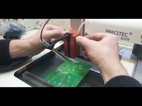
Update: Just realized that placing the P2 onto the paste without smudging is going to be tricky without special place tools. Tweezers may not be sufficient. All other parts will be okay.
Hardest part is done (by hand). Just have to hope the solder globs I fed through the hole to the ground made good connection underneath. Time will tell. Is there some way to check ground has made connection to the P2 before power up?
It would be pretty hard to know before powering up, unless you have a couple of isolated vias that aren't directly connected to the ground plane
When powering up remember you should see something like 30mA for a minute or so before the chip goes into power down. So you could set a reasonably low current limit on your supply
@rogloh said:
Hardest part is done (by hand). Just have to hope the solder globs I fed through the hole to the ground made good connection underneath. Time will tell.
>
Wow! If my eyes where that good, I'll could candidate myself for a Brain (Salad (EL&P)) Surgery vacancy, at any big hospital!
Is there some way to check ground has made connection to the P2 before power up?
At each of the four corners of the package, there is a little protruding remainner of the internal wireframe GND-square-ring. Perhaps needs some grasping, with a sharp blade, in order to ensure good contact, but, since there are one at each corner, you can slightly uncover all of them, and perform a cross-test, so as to make sure you're really reaching the right spot, before checking against the land patternexposed pad connection to any other point at the board, where GND can be accessed.
Hope it helps, and also good luck!
P.S. In order to be clear: any check/test of the land pattern connection to GND at the heat spreader that doesn't really evaluate the amount of solder coverage/interconection between board's land patern and package exposed pad coud be understood as the same thing like as attempting a Bungee Jump, while tyed to Dental Floss!!!
X-Ray inspection is the best test-method ever in that case. (period)
@Tubular , yeah I'll be limiting the current the first time it's powered on.
Wow, thanks Yanomani. Didn't realize that. I just probed and found continuity between 3 of the 4 corners (one might not be protruding far enough for proper contact), but no continuity from there to GND.
Maybe I need to reheat the ground hole.
Are you 100% sure this contact point at the corners is a GND?
EDIT: I just reheated the GND hole solder and saw some flux bubbling up through the vias and now I do have continuity to GND from those corner spots. Awesome. Thanks Yanomani, that saved some amount of grief.
Only thing I don't like is that I measured ~2.5 ohms via this path. Is that to be expected or is my GND a bad connection?
Sorry for the long delay: I was having trouble with my old TENMA meter probes; one of them (just the GND one) broke its neck, and the corresponding wire just disconnected. It's a now 33 y.o. Paralympics VOM silver medallist, because it's still good for a reading at the lowest Ohm range.
At least at my Rev B chip, all four corners are in good/full contact (near Zero Ohm, Lona, Nada) with the exposed pad and the underlying "inner guts".
The ~2.5 Ohm reading is not any good, you should be having a bad contact somewhere else, including the exposed pad.
Did you spreaded at least some kind of a layer of fresh solder paste at any of the pcb land pattern, or the exposed pad, before seating the package onto the pbc?
Addit: doesn't you have any no clean solder flux for reflow, compatible with the solder paste you're using (perhaps Kester 951 (lead free), Kester 186 (rosin) or other good similar)?


Comments
I might wait for measuring this as I need to break open another moisture sealed package for that.
I re-measured the resistance between my RES pin (in theory attached to PG) and GND. It's now infinite in both directions when the probes are swapped over. Weird. I'm starting to wonder what is different to before and it is introducing some doubt...perhaps I temporarily energized the input cap when probing resistance before...?
Update: yes that was almost it. Turns out I energized the output cap when probing for a short on 1.8V output and that caused the PG to be driven low. I can make this happen, and also later float the PG pin when I short the output cap with tweezers. I guess this means the PG pin is actually connected to the device if it is having an effect like this.
Perhaps some residual charge remainned at the capacitors, during the initial measurements, since there was no real current consumption.
See above for update.
Thanks for the update, and it also means "Hey, I'm not feeling any good. Watch out!" from a voltage regulator standpoint.
I was able to get 0.3V out again on the VOUT pin. But again as soon as I added the 47 ohms of load, it dropped to zero. If I measure it after removing that resistance and wait a while I see the output voltage slowly climbing. It's rising to 0.08V after a few minutes or so and still continuing. I have no idea what it's doing really at this point in time. Maybe the switching regulator output cap is bad or an incorrect value or the FB pin is floating and causing issues.
Without the help of a microscope, it would be very hard to tell if the yolks and white parts of that "egg" got messed, during the reflow proccess. I don't know if a really good camera, armed with a macro lenses can be of any use, when trying to spot any extra-molten or shorted parts.
Addit: at page 11 of the datasheet, fig. 8-1, you can see a graph, showing the conditions/trip-points for PG reaction.
Does that vary with probe polarity ?
Usually the substrate diode is more obvious in one direction, and that has a diode drop, more obvious if you force ranges on the meter (thus change the test current).
On my more accurate meter now I just measured 36.5 and 37.5 ohms for each probing direction so basically close enough to be the same. Variation is probably due to how hard I push down on the board.
I think later today I might try a second board attempt and see if I get a better result...
This is the current solder paste I am using also:
https://www.farnell.com/datasheets/1770478.pdf
I think the profile is okay with my PCB heater, though it might heat up at a slightly slower rate like 4mins instead of 3mins. Haven't fully measured measured that as to date I've had my hands full with the thermocouple alone. Be good to automate the measurement. I yank the board off the plate once it peaks in temp and let it cool down by itself and it cools quite quickly.
That sounds a bit suspicious - can you probe an unmounted part, each way, to compare ?
Addit: maybe mount just the SMPS chip and caps on a board, and check that ? Probe of an unmounted part could also confirm, the pin-footprint is 100% correct.
+1
Once I open another package up I can try that. But for it to occur I needed to first energize the VOUT pin slightly on my board by measuring the resistance to ground of VOUT at the output cap which charges the output voltage slightly, otherwise PG floats, so it may not do much when I directly measure a standalone part's PG pad. I also recently measured that output cap (in circuit) and it measured 22uF as expected. The impedance to ground via the VOUT pin through the integrated inductor is over 28Mohms which is why the capacitor reading worked. But I can't read the VIN input capacitance in circuit though and get 0nF, the regulator's input impedance must be preventing this measurement. Also I found that the integrated inductor has continuity through it, in case that path was broken on the board.
Here's an example of the solder paste wall edge quality I had today. Seems reasonable to me, but I'm no expert there. It does appear to hold its edge, but I'm not sure for how long as I placed the components on very soon after this.
I've just cooked up another P2ME2 board and can try later tonight to see if I have better luck with its regulator or have the same issue again.
I timed it from room temp and the hotplate took 260 seconds to reach solder melt of 183C and about another minute to get up to 210C before I removed the board to cool it down (according to the paste specs).
Just tried it. 1.82V at the regulator output. YES!
Now I wish I loaded more parts. LOL
Great")
Hehe, that's the way you guarantee it will work ok")
Congratulations, and +1 to jmg's comment too!!!
@rogloh, when it's fully setup and running, the whole cannibal tribe is planning a get togheter, for a meal, in honor to your pcb's success.
For obvious reasons, outlanders will get no invitations: the menu for the great day just says "complete"
Thanks Yanomani.
I just removed the 3.3V LDO from the first "bad" board and added it to my second "good" board to salvage the part and avoid reorder delay, still seems to work which is good.
Next I plan to check the ridiculously tiny 1.8V regulator can indeed supply ~2A at 1.8V and see how hot it might get doing so. Then when I know it can do this I will hand solder on a P2 and try to boot it up with a prop plug. I just hope I remembered to extend the P2 pads out slightly for doing the hand soldering. I typically do that on my boards but can't recall if I did this or not. If I didn't it's going to be more difficult to hand solder and I'll probably need to cook up a fully loaded board and hope for the best again. But the latter approach is probably a much faster way to go though and also saves my eyes.
You're welcome!
Seventeen years ago, I used to share an associate/friend's lab, where he had many reballing kits at hand, because he's a master on the art of smt board repair.
Each kit comes with its own set of solder paste spreading masks, intended to viabilize the requerid many-step proccess, one of them involving the application of a fresh set of solder balls onto a just-removed-and-cleaned bga package.
Since you know about that all, I'll try to be short: can't you use the metal solder mask, and apply a bit of solder paste just over all P2 pads, sure, by having it (P2, standing bottom up), layd onto a flat surface?
In case of a positive answer, wouldn't a proccess like the above just easy the hand soldering task a little bit?
I think having some components already soldered on doesn't work out well with this idea because the metal stencil won't sit flat enough on the rest of the board to be able to reliably squeegee on the paste. I don't really want to cut the stencil up either.
It would speed things up yes if it was possible. But I do have just enough parts for a third full attempt.
I just learned it from another perspective: If you prepare a fossil, the last beat is always one to much. So be happy as it is ;-)
My fuzzy english skills got me again...
I refered to "P2 pads" when I was intending to say "P2 pins". Sorry, it was my fault!
The "sure, by having it (P2, standing bottom up), layd onto a flat surface?" part was meant to clarify it a bit, without success...
I should have realized that the mask you're using is way bigger than the ones we handled in BGA reballing, so there must be some kind of thick mask around the LQFP package, or a cavity at the surface, for that proccess to have a real chance. My bad...
I see what you mean now. It's an interesting idea to try to put paste onto the P2 leads that way. Would probably suit hot air rework method if it was doable.
I'm tempted to just hope for a good third result with the P2 and bypass caps etc installed this time. I now think the reason that the first board's regulator probably failed was there was a little less paste applied on that board and a void formed under the EN pin and it floated. The second board definitely had more paste on it and that might have been the key to getting it working.
Great news that it worked. Yeah I think I'd jump to the third board too. Then, if fit doesn't work, you can always cut the stencil in half and come back to the second one
I found a bit of a trick with the stencils - belatedly. If you go with defaults you end up with the stencil like you have, which is shipped separate to the other pcbs, and charges extra for shipping. However if you go down the 'custom stencil size' path, I was able to specify 100x100mm, which then ships free with the rest of the pcbs
Yeah I think when I ordered a different PCB from PCBWay with a stencil some time ago it all came in the one shipment which was good. It wasn't nearly as large as this one stencil either. Most of that metal gets wasted with such a small board, though the excess overlap can help it stay nice and flat when you apply the paste.
Just wishing a lot of good karma, from the best of our "Xamãs"!
https://youtu.be/mpjs83ShhA0
I ran this 1.8V regulator at about 1.7-1.8A output for a while - it's difficult to load up fully with just small value resistors I have so I partially resorted to using the lead resistance of my ammeter itself as a load. It got a little warm but not really hot so I think the thermals should be sufficient to take the next step. Efficiency seemed to be about 90% or so but the current wasn't fully stable in my probing setup so I probably need to take better readings later. I did hear some faint microphonic(?) vibration when the board was pressed down onto the table surface under load.
Time to cook a full board I think...
Update: Just realized that placing the P2 onto the paste without smudging is going to be tricky without special place tools. Tweezers may not be sufficient. All other parts will be okay.
One of these would be nice...
Hardest part is done (by hand). Just have to hope the solder globs I fed through the hole to the ground made good connection underneath. Time will tell. Is there some way to check ground has made connection to the P2 before power up?
It would be pretty hard to know before powering up, unless you have a couple of isolated vias that aren't directly connected to the ground plane
When powering up remember you should see something like 30mA for a minute or so before the chip goes into power down. So you could set a reasonably low current limit on your supply
Looks pretty good from here though
>
Wow! If my eyes where that good, I'll could candidate myself for a Brain (Salad (EL&P)) Surgery vacancy, at any big hospital!
At each of the four corners of the package, there is a little protruding remainner of the internal wireframe GND-square-ring. Perhaps needs some grasping, with a sharp blade, in order to ensure good contact, but, since there are one at each corner, you can slightly uncover all of them, and perform a cross-test, so as to make sure you're really reaching the right spot, before checking against the land pattern exposed pad connection to any other point at the board, where GND can be accessed.
Hope it helps, and also good luck!
P.S. In order to be clear: any check/test of the land pattern connection to GND at the heat spreader that doesn't really evaluate the amount of solder coverage/interconection between board's land patern and package exposed pad coud be understood as the same thing like as attempting a Bungee Jump, while tyed to Dental Floss!!!
X-Ray inspection is the best test-method ever in that case. (period)
@Tubular , yeah I'll be limiting the current the first time it's powered on.
Wow, thanks Yanomani. Didn't realize that. I just probed and found continuity between 3 of the 4 corners (one might not be protruding far enough for proper contact), but no continuity from there to GND.
Maybe I need to reheat the ground hole.
Are you 100% sure this contact point at the corners is a GND?
EDIT: I just reheated the GND hole solder and saw some flux bubbling up through the vias and now I do have continuity to GND from those corner spots. Awesome. Thanks Yanomani, that saved some amount of grief.
Only thing I don't like is that I measured ~2.5 ohms via this path. Is that to be expected or is my GND a bad connection?
Sorry for the long delay: I was having trouble with my old TENMA meter probes; one of them (just the GND one) broke its neck, and the corresponding wire just disconnected. It's a now 33 y.o. Paralympics VOM silver medallist, because it's still good for a reading at the lowest Ohm range.
At least at my Rev B chip, all four corners are in good/full contact (near Zero Ohm, Lona, Nada) with the exposed pad and the underlying "inner guts".
The ~2.5 Ohm reading is not any good, you should be having a bad contact somewhere else, including the exposed pad.
Did you spreaded at least some kind of a layer of fresh solder paste at any of the pcb land pattern, or the exposed pad, before seating the package onto the pbc?
Addit: doesn't you have any no clean solder flux for reflow, compatible with the solder paste you're using (perhaps Kester 951 (lead free), Kester 186 (rosin) or other good similar)?