@jlsilicon said:
Previosly ...
Cute board articles, but no Gerbers ... ?
Yeah I didn't release the Gerbers so far. I wonder if I should now the regulators I used have become available again and in theory this board could be built again. It had limitations and was tricky to assemble by hand but it did work in the end after many problems to solve along the way.
If you really wanted to make one I could potentially send you a couple of blank P2ME2 boards, depending on where you are in the world and postage costs. I might have a few spares left over and can always make more but I'll need to check how many I initially made.
update: I have a couple of spares if you want. PM me.
If you really want to avoid switching regulators, I'd suggest select a large-package TAB=GND part that you mount on the rear side, copper poured.
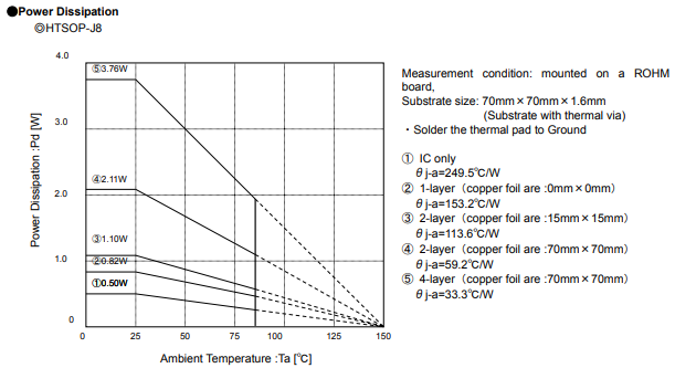
4 Layer board helps a lot with cooling, and with decoupling. (see ROHM data below)
You can use 3 regs : 3v3 for IO, and another 3v3 for power spread to a 1.8V reg. That keeps the core noise away from IO.
Parts with PowerGOOD ensure things only run when VCC is ok.
Perhaps a 39301 or 59151 or 29371 etc or maybe a SO8EP part.
PCB cooling example :
If you can manage QFN20, a regulator like AP7179 has some nice 'modern' features : Low noise, very low TJC, pin strap Vout, 1% set, PowerGOOD.
High data rates can be the biggest power draw but my testing wasn't practical example. It mainly utilised 100% hubRAM bandwidth to achieve the extreme loading. Each Streamer reading alternating hubRAM bit pattern at sysclock frequency and piping that data out to pins but with final floating pin drive so that VIO wasn't counted and comms not corrupted.
The remaining load came from all Cogs + Cordic compute in a tight loop using GETRND data but that was much smaller loading up against the Streamers.
The best example of real use that pushes power consumption is Ada's Neoyume emulator. It also heavily utilises bulk data copies and larger data sets in PSRAM with most Cogs participating.
PS: I never actually got a definitive measurement in my testing. I'd measured up to 5.5 Watts @ 360 MHz but I later learned of a bug that meant I couldn't be sure that all Cogs had even got running. There wasn't any reporting in the code to verify the steps. It's something to circle back round to I guess ...
PPS: 5.5 Watts means approx 3.0 Amps on VDD. That's overloading even the Eval Board 1.8 Volt regulator. Any further testing will be at slower clock. I had to use freezer packs as it was anyway. That wasn't much fun after the first attempt.
@jlsilicon said:
I do not know until I program it.
I was aiming to use it for AI and Vision Recognition processing ...
I moved over to Lm1117-3.3 , Lm1117-1.8 - seem to provide 800mA each.
That will still be too light for the 1.8V path, but could be ok for 3.3V alone.
Lower noise 3.3V regulators are often chosen for 3.3V. eg a AP2114HA has GND tab, or the RP108Jxx in TO-252-5 comes in 1v8 and 3v3 models and can deliver > 3A peak
If you allow a 2A or even 3A peak pathway for 1.8V, you can simply add airflow, if you later find you are pushing things.
If you spread packages like TO-252 under the board, you can bolt the board onto a metal spreader, using the package as spacers, for double sided cooling.
@jlsilicon Your DIL-version looks very similar to my KISS board. I've quit selling them because there were too much complaints about them not running very well above 300MHz and with external RAM. But I still have plenty of them, ~100 empty PCBs and @ErNa should have lots of assembled boards. If you are interested I could send you the Eagle and gerber files for free or the PCBs for the raw material price.
Your board IMHO has very little ground connections and much fewer decoupling caps than mine so I doubt it will run any better with overclocking.
I agree, every design needs some circling around and if the goal is not to run such circles but to create an application, sourcing boards is an advantage. Indeed, I have some KISS boards in stock I didn't use myself now, but will do over the time, so I'm not actively looking for customers.
I have used the Aps6404 by bitbanging & SPI & DMA on my W806 240MHz Micros.
-- But, I skipped the special board - just mounted them on Dip8 boards with WireWrap pins - so I could Stack 'em .
... Easy and quick to make.
That's only slightly better, with no improvement in cooling. You need a lot better.
Since your design seems to be more thru hole focused, and 2 layer, with minimal copper, you could shift the thermal challenges by using a package like this
You then mount those tab-down onto a heatsink, and form the leads up to solder thru the PCB.
My suggestion (at least for 1v8) would be to use the MEZD7 series switching regulators, which follow the 7805 footprint, and are available in 1, 2 or 3A output currents
@Tubular said:
My suggestion (at least for 1v8) would be to use the MEZD7 series switching regulators, which follow the 7805 footprint, and are available in 1, 2 or 3A output currents
That certainly saves design time, if a little chunky.
Even the DC-DC switchers on the P2ME2 and KISS boards are quite simple things, with easy to use packages.
Yes easy if you're used to such packages.
I guess my more important point is that if you're using 3 x 0.1" holes, going with the 7805 style "IN-GROUND-OUT" has lots of pre-built options, such as MEZD7 series, Recom (quite cheap), and others.
There's not as many prebuilt switchmode options in the 1117 style GROUND-OUT-IN pin ordering
@jmg said:
Even the DC-DC switchers on the P2ME2 and KISS boards are quite simple things, with easy to use packages.
On P2ME2 the regulators I used were easy to design with yes but pretty small physically. Fairly difficult to hand solder with an iron tip (hot air soldering would be simpler), and the 10 pin one needed a hotplate or oven and a well aligned stencil. The pads on that one were tiny! Am looking at a board right now.
One issue with P2 that had to sort through is that 1.8 and 3.3 V power demands grow pretty large as clock freq. gets near or past 300 MHz.
At ~160 MHz or so, simple regulators are probably fine.
Above, that things start getting hot.
Fortunately, I found some low cost switching regulators from Microchip that keep things cool.
Unfortunately, those are not good for analog outputs.
So, my compromise was to have certain pin groups with LDO and the rest on the switching regulator...
@rogloh said:
On P2ME2 the regulators I used were easy to design with yes but pretty small physically. Fairly difficult to hand solder with an iron tip (hot air soldering would be simpler), and the 10 pin one needed a hotplate or oven and a well aligned stencil. The pads on that one were tiny! Am looking at a board right now.
Yes, I'd forgotten about that one, I was looking at the 6 pin one.
Cutting edge today seems to be as low as 10-mΩ, and 6A pk, for the little SOT-563 parts
TPS62A06x, 6-A, SOT563 2.5-V to 5.5-V Vin 15-mΩ / 10-mΩ switches (6 A) 2.2-MHz switching frequency TI $0.267 | 1ku
tho lcsc show some useful TSOT-23-6 parts, with low RDS fets
TPS565201DDCR 4.5V~17V 5A 0.6V~7V TSOT-23-6 DC-DC Integrated 31-mΩ and 16-mΩ FETs 100+ US$0.3119
RT6255BHGJ6F Richtek Tech 4.5V~18V 5A 0.6V~5V SOT-23-6 Internal 45mΩ Switch and 23mΩ 100+ US$0.3135
I don't blame you. I did a Samtec 0.5mm connector once by hand and it wasn't fun. Probably took over an hour to get right as it took me ages to cleanup all the bridges between legs which had managed to wick themselves underneath the legs of the part where I couldn't reach with the iron. Used heaps of flux and braid to get it out in the end (also gravity helps too). The little 6 pin SOT-563s can be quite bad too if you add too much solder. My trick now is to only feed the tiniest amount of solder in at the start and let it wick onto the leg itself from there. But things have to be clean for it to work out.
I have a fine-tip soldering iron - that I use for touch soldering Large chips down to 0.5mm .
But, not the tiny transisors and resistors - if I can avoid it.
@jlsilicon said:
Why not just solder the P2 chip upside-down to a so etched board,
then mount a heatsink on top (or the now bottom up) P2 ...
Not sure I completely understand what you mean unless you planned to face the bottom of the chip outwards towards free air but you will still need the main square in the middle of the P2 as the ground pad so it makes electrical connection. Are you considering grounding through a heatsink itself?
Prolly hadn't sunk in that all VSSs and GIOs are only connected through the thermal pad.
Here's a photo of a Prop2 without its top moulding. The metal ring that runs right around in between the pins and the die is a pressed-raised part of the thermal pad. If you look carefully you'll be able to verify that each VSS jumper and each GIO jumper is welded to that ring. None of which go to any pins.
A trivia: The creamy coloured area, the bulk of the die, is the synthesised logic area - fabricated from Verilog code. The darker square ring around that is the custom pad-ring that was laid out by hand. Each transistor having dimensional and doping attributes to define it's desired characteristics. And things like track widths defining current carrying capacity.
I vaguely remember Chip saying there is four metal layers in the fabrication. Presumably that's a small number to keep cost down.
@jlsilicon said:
Why not just solder the P2 chip upside-down to a so etched board,
then mount a heatsink on top (or the now bottom up) P2 ...
Not sure I completely understand what you mean unless you planned to face the bottom of the chip outwards towards free air but you will still need the main square in the middle of the P2 as the ground pad so it makes electrical connection. Are you considering grounding through a heatsink itself?
It just takes a little creativity :
Turn the chip upside-down
(yes, face down, won't be able to see the P2 emblem because its face down on the board now) ;
Bend the pins down slightly - and solder them to the Reverse board chip pattern ;
Tie/solder the now top Gnd plane with wires back to the Board ;
Mount / solder a Large Heatsink / wind-tunnel on the now Top (chip bottom Gnd plane) etc.
Instead of bending pins, what about routing out a hole in the board to drop the P2 through? Or use a socket that's extended enough to accept the P2 upsidedown.
Probably you thought of these things- curious what conclusions you came to
@VonSzarvas said:
Instead of bending pins, what about routing out a hole in the board to drop the P2 through? Or use a socket that's extended enough to accept the P2 upsidedown.
Probably you thought of these things- curious what conclusions you came to
That is the original idea - look at the board - with the Routing Holes.
I was suggesting an easy alternative method.
-- My point to the upside-down method ,
is that the Bottom board space is now Untouched - for other parts .
And, you have the full chip Gnd Plane open for soldering / mounting / etc ;
-easy direct access now to mount a Heatsink.
: Engineer's motto - 'To always find a better way ...'
: Engineer's motto - 'To always find a better way ...'
Well, I'd say find a way that works first and then improve on it only if it doesn't work good enough in the first place (for the intended purpose) . If it does then maybe it doesn't need improvements.
@jlsilicon said:
It just takes a little creativity :
Turn the chip upside-down
(yes, face down, won't be able to see the P2 emblem because its face down on the board now) ;
Bend the pins down slightly - and solder them to the Reverse board chip pattern ;
Tie/solder the now top Gnd plane with wires back to the Board ;
Mount / solder a Large Heatsink / wind-tunnel on the now Top (chip bottom Gnd plane) etc.
QED
I'm sure the production engineering department would be smiling too...
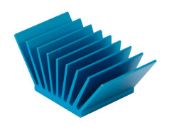
They might even suggest a heatsink you could use - these are surprisingly low cost on aliexpress.
The P2 die and plastic are large enough, and the package thin enough, that a top mounted heatsink can work quite well, without package gymnastics
Especially if you have added moving air.
Here is one example of a top-of-P2 candidate (normal mounting) 17mm square at the base. ( at 400 LFM=4.2°C/W )


Comments
Yeah I didn't release the Gerbers so far. I wonder if I should now the regulators I used have become available again and in theory this board could be built again. It had limitations and was tricky to assemble by hand but it did work in the end after many problems to solve along the way.
If you really wanted to make one I could potentially send you a couple of blank P2ME2 boards, depending on where you are in the world and postage costs. I might have a few spares left over and can always make more but I'll need to check how many I initially made.
update: I have a couple of spares if you want. PM me.
If you really want to avoid switching regulators, I'd suggest select a large-package TAB=GND part that you mount on the rear side, copper poured.
4 Layer board helps a lot with cooling, and with decoupling. (see ROHM data below)
You can use 3 regs : 3v3 for IO, and another 3v3 for power spread to a 1.8V reg. That keeps the core noise away from IO.
Parts with PowerGOOD ensure things only run when VCC is ok.
Perhaps a 39301 or 59151 or 29371 etc or maybe a SO8EP part.
PCB cooling example :
If you can manage QFN20, a regulator like AP7179 has some nice 'modern' features : Low noise, very low TJC, pin strap Vout, 1% set, PowerGOOD.
High data rates can be the biggest power draw but my testing wasn't practical example. It mainly utilised 100% hubRAM bandwidth to achieve the extreme loading. Each Streamer reading alternating hubRAM bit pattern at sysclock frequency and piping that data out to pins but with final floating pin drive so that VIO wasn't counted and comms not corrupted.
The remaining load came from all Cogs + Cordic compute in a tight loop using GETRND data but that was much smaller loading up against the Streamers.
The best example of real use that pushes power consumption is Ada's Neoyume emulator. It also heavily utilises bulk data copies and larger data sets in PSRAM with most Cogs participating.
PS: I never actually got a definitive measurement in my testing. I'd measured up to 5.5 Watts @ 360 MHz but I later learned of a bug that meant I couldn't be sure that all Cogs had even got running. There wasn't any reporting in the code to verify the steps. It's something to circle back round to I guess ...
PPS: 5.5 Watts means approx 3.0 Amps on VDD. That's overloading even the Eval Board 1.8 Volt regulator. Any further testing will be at slower clock. I had to use freezer packs as it was anyway. That wasn't much fun after the first attempt.
That will still be too light for the 1.8V path, but could be ok for 3.3V alone.
Lower noise 3.3V regulators are often chosen for 3.3V. eg a AP2114HA has GND tab, or the RP108Jxx in TO-252-5 comes in 1v8 and 3v3 models and can deliver > 3A peak
If you allow a 2A or even 3A peak pathway for 1.8V, you can simply add airflow, if you later find you are pushing things.
If you spread packages like TO-252 under the board, you can bolt the board onto a metal spreader, using the package as spacers, for double sided cooling.
Some great PCB area info here
https://fscdn.rohm.com/en/products/databook/applinote/ic/power/linear_regulator/to252_thermal_resistance_information_an-e.pdf
@jlsilicon Your DIL-version looks very similar to my KISS board. I've quit selling them because there were too much complaints about them not running very well above 300MHz and with external RAM. But I still have plenty of them, ~100 empty PCBs and @ErNa should have lots of assembled boards. If you are interested I could send you the Eagle and gerber files for free or the PCBs for the raw material price.
Your board IMHO has very little ground connections and much fewer decoupling caps than mine so I doubt it will run any better with overclocking.
I agree, every design needs some circling around and if the goal is not to run such circles but to create an application, sourcing boards is an advantage. Indeed, I have some KISS boards in stock I didn't use myself now, but will do over the time, so I'm not actively looking for customers.
How about Adp3338 VReg ?
I am impressed with your 64MB PSRAM board.
I have used the Aps6404 by bitbanging & SPI & DMA on my W806 240MHz Micros.
-- But, I skipped the special board - just mounted them on Dip8 boards with WireWrap pins - so I could Stack 'em .
... Easy and quick to make.
That's only slightly better, with no improvement in cooling. You need a lot better.
Since your design seems to be more thru hole focused, and 2 layer, with minimal copper, you could shift the thermal challenges by using a package like this
You then mount those tab-down onto a heatsink, and form the leads up to solder thru the PCB.
My suggestion (at least for 1v8) would be to use the MEZD7 series switching regulators, which follow the 7805 footprint, and are available in 1, 2 or 3A output currents
Latest Rev of P2DIP3 board :
That certainly saves design time, if a little chunky.
Even the DC-DC switchers on the P2ME2 and KISS boards are quite simple things, with easy to use packages.
Yes easy if you're used to such packages.
I guess my more important point is that if you're using 3 x 0.1" holes, going with the 7805 style "IN-GROUND-OUT" has lots of pre-built options, such as MEZD7 series, Recom (quite cheap), and others.
There's not as many prebuilt switchmode options in the 1117 style GROUND-OUT-IN pin ordering
On P2ME2 the regulators I used were easy to design with yes but pretty small physically. Fairly difficult to hand solder with an iron tip (hot air soldering would be simpler), and the 10 pin one needed a hotplate or oven and a well aligned stencil. The pads on that one were tiny! Am looking at a board right now.
One issue with P2 that had to sort through is that 1.8 and 3.3 V power demands grow pretty large as clock freq. gets near or past 300 MHz.
At ~160 MHz or so, simple regulators are probably fine.
Above, that things start getting hot.
Fortunately, I found some low cost switching regulators from Microchip that keep things cool.
Unfortunately, those are not good for analog outputs.
So, my compromise was to have certain pin groups with LDO and the rest on the switching regulator...
Yes, I'd forgotten about that one, I was looking at the 6 pin one.
Cutting edge today seems to be as low as 10-mΩ, and 6A pk, for the little SOT-563 parts
TPS62A06x, 6-A, SOT563 2.5-V to 5.5-V Vin 15-mΩ / 10-mΩ switches (6 A) 2.2-MHz switching frequency TI $0.267 | 1ku
tho lcsc show some useful TSOT-23-6 parts, with low RDS fets
TPS565201DDCR 4.5V~17V 5A 0.6V~7V TSOT-23-6 DC-DC Integrated 31-mΩ and 16-mΩ FETs 100+ US$0.3119
RT6255BHGJ6F Richtek Tech 4.5V~18V 5A 0.6V~5V SOT-23-6 Internal 45mΩ Switch and 23mΩ 100+ US$0.3135
I don't solder those 0.5mm chips
I don't blame you. I did a Samtec 0.5mm connector once by hand and it wasn't fun. Probably took over an hour to get right as it took me ages to cleanup all the bridges between legs which had managed to wick themselves underneath the legs of the part where I couldn't reach with the iron. Used heaps of flux and braid to get it out in the end (also gravity helps too). The little 6 pin SOT-563s can be quite bad too if you add too much solder. My trick now is to only feed the tiniest amount of solder in at the start and let it wick onto the leg itself from there. But things have to be clean for it to work out.
I have a fine-tip soldering iron - that I use for touch soldering Large chips down to 0.5mm .
But, not the tiny transisors and resistors - if I can avoid it.
Why not just solder the P2 chip upside-down to a so etched board,
then mount a heatsink on top (or the now bottom up) P2 ...
Not sure I completely understand what you mean unless you planned to face the bottom of the chip outwards towards free air but you will still need the main square in the middle of the P2 as the ground pad so it makes electrical connection. Are you considering grounding through a heatsink itself?
Prolly hadn't sunk in that all VSSs and GIOs are only connected through the thermal pad.
Here's a photo of a Prop2 without its top moulding. The metal ring that runs right around in between the pins and the die is a pressed-raised part of the thermal pad. If you look carefully you'll be able to verify that each VSS jumper and each GIO jumper is welded to that ring. None of which go to any pins.
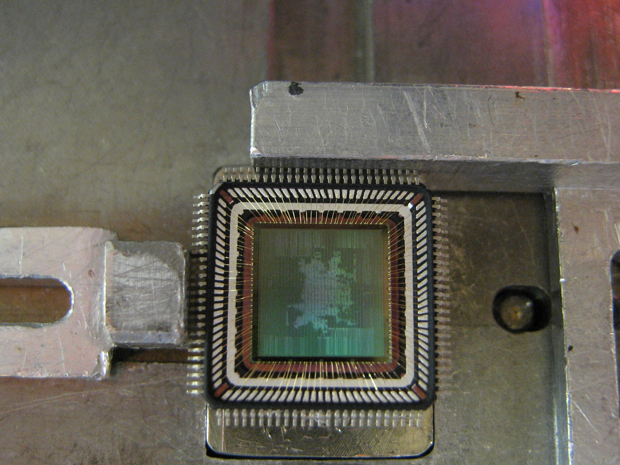
A trivia: The creamy coloured area, the bulk of the die, is the synthesised logic area - fabricated from Verilog code. The darker square ring around that is the custom pad-ring that was laid out by hand. Each transistor having dimensional and doping attributes to define it's desired characteristics. And things like track widths defining current carrying capacity.
I vaguely remember Chip saying there is four metal layers in the fabrication. Presumably that's a small number to keep cost down.
It just takes a little creativity :
(yes, face down, won't be able to see the P2 emblem because its face down on the board now) ;
QED
Instead of bending pins, what about routing out a hole in the board to drop the P2 through? Or use a socket that's extended enough to accept the P2 upsidedown.
Probably you thought of these things- curious what conclusions you came to
That is the original idea - look at the board - with the Routing Holes.
I was suggesting an easy alternative method.
-- My point to the upside-down method ,
is that the Bottom board space is now Untouched - for other parts .
And, you have the full chip Gnd Plane open for soldering / mounting / etc ;
-easy direct access now to mount a Heatsink.
: Engineer's motto - 'To always find a better way ...'
Well, I'd say find a way that works first and then improve on it only if it doesn't work good enough in the first place (for the intended purpose) . If it does then maybe it doesn't need improvements.
LOL - Thats why I am so successful ...
I'm sure the production engineering department would be smiling too...

They might even suggest a heatsink you could use - these are surprisingly low cost on aliexpress.
The P2 die and plastic are large enough, and the package thin enough, that a top mounted heatsink can work quite well, without package gymnastics
Especially if you have added moving air.
Here is one example of a top-of-P2 candidate (normal mounting) 17mm square at the base. ( at 400 LFM=4.2°C/W )