

P2DIP1 Board Design
 System
Posts: 46
System
Posts: 46
This discussion was created from comments split from: P2D2 - An open hardware reference design for the P2 CPU.
Edit: 2023.12.06. Thread renamed at request of OP.
Edit: 2023.12.06. Thread renamed at request of OP.
Comments
Not using USB or RTC :
X - USB
X - EFM8UB3
X - TPS22919
? - MPM38111GR
X - Si5351A
X - RV3028
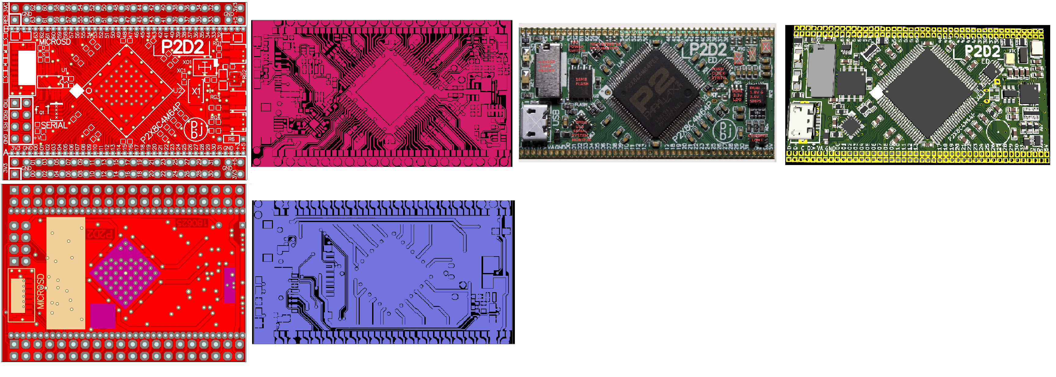
Left Brd is old Brd with Serial Hdr Dip , Right is PCB , PCB populated :
DipTrace is good , except that it is not displaying the DrillHoles.
GerbView does not import the DRL/DRR files either.
Try KiCAD's Gerber editor.
I am confused here.
I am comparing the Gerbers with the P2 pinout and the Schematic.
They don't seem to match.
Gerbers have the Vdd , VA , VB linked to Port pins.
I am using the board photo, and the Xtal p50 & p51 Xtal pins as verify.
No matter how you rotae the chip , the gerbers do not match the pinout.
And NO Gnd pins - just the Base ? ... GMAB
So, now I had to Drill through the Bottom of my Breakout Board (with the already soldered down P2 chip) to get to the Gnd ,
because I did not know this.
-- I felt like Matt Damon in The Martian drilling through the Mars buggy roof ...
Just base is ground.
Every four io pins has own 1.8v and 3.3v supply…
They don't seem to match.
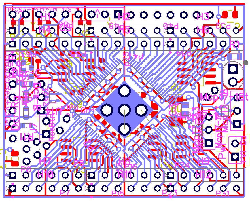
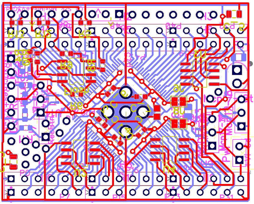
This is my start from scratch design :
This is the Pinout from one of the Parallax Schematics :
That ring around the ground pad is probably 1.8 v bus and all the vias next to it are probably 3.3 v (or reverse of that)
Oh, this is your design. I get it now. This doesn't look like later p2d2.
One thing that was learned is that need a lot of vias under ground pad if want to get above 300 MHz...
I got that , but compare the first multi image, the pins don't corelate.
I followed the P2 chip pinout (my print is Cyana now Reveresed).
Red Print is the Gerbers from here p26.
Look , I matched RxTx on Left anf XTal on the Right ,
but I need to Reverse the Image to match the Vdd , V3.3 , V1.8 pins - ???
Count the Vdd , V3.3 , V1.8 , the Gerber has them mounted backwards (Red).
My print is Cyana , I needed to drop it in Reverse, but now the RxTx and XTal pins are on the Wrong side.
It looks like the Gerbers are mounted backwards compared to RxTx and Xtal Pins sides.
P2 Pinout :
100 - ResN
99 - Rx
98 - Tx
97 - +V6063
96 - p61
95 - p60
94 - +Vdd
I guess you could look at the Gerbers that I posted here to see if that helps:
https://forums.parallax.com/discussion/175353/next-attempt-at-a-board-that-can-hit-340-mhz-it-works/p1
I don't really use Gerbers other that for getting boards made, so don't know if it's a mirror image or something...
But, I did post screenshots of my boards layers in latest posts in above thread...
I'm not sure where the confusion is, the red gerbers above look OK to me. That fat ring around the ground pad is Vdd (1v8).
I think the RX and TX (physical pins 99 and 98) go out to the top left of the board where the breakout header is, before winding their way back to the USB chip at lower left.
I have an early P2D2 board that we did a lot of testing with, so can confirm it did indeed work successfully. I'm happy to check anything on it if that would help
If red is your top layer in your start-from-scratch design, then its definitely not correct.
When looking at the P2 chip from above (with ground pad underneath and not visible), the pin count increases in a counterclockwise direction
Is this upsidedown then ? :
Are you kidding me ??
Okay, I flipped my Print , I need to check parts pinouts though :
Interesting Board, thx.
Cool, you used the Aps6404 - wow 8 of them - 64MB.
You put a Cap on every Port pin ?
May try the VGA -else HDMI as an Expansion board.
There’s also a place on bottom for extra cap on each pin .. didn’t seem to help anything so far though
Yeah unfortunately that is indeed upside down, as if looking at the bottom of the chip.
Don't forget the pullup resistor on the RESn line - the P1 doesn't need it but the P2 does. You might already have it there on your new design, I couldn't be sure
I think you meant power pin ?
If you make a 4 layer design, you may be ok with fewer caps on underside.
Very small caps can fit more in, but are harder to manually assemble.
My finalized first board version for the P2 chip.
Ports busses 64bits : P0-31 on bottom bus , P32-P63 on top bus - on 2nd & 3rd rows,
-- including +3V & Gnd pins on corners (except Lower Right which is +VIn).
SD Card pins - for attaching a Micro SD Card board (Extending Out from Board from Top -and/or- Toward Center underneath)
-- on the top bus , next to spare pins on upper right side.
Serial Bus including +3V In , and 2n3904 Res on left side.
-- Does it look correct , usable ?
-- Did I forget anything ?
Top print visible :
Bottom print visible :
These 2 Prints are the TopView Overlays of Top and Bottom - Not Flipped.
-- Excuse any mistakes - its just a quick job.
-- No Audio or Video circuits - sorry.
-
And, the Gerbers :
Not really, no. See below.
There are built in caps. Many designs allow for xtal package options, including 4 pin Oscillator modules, that then allow TCXO choices.
As P2 designs go, that is seriously under-provided !!.
Those look like feeble TO-92 Linear regulators ?
I only see 2 caps on the 1v8 ?
Any inner planes ?
No copper pour ?
The annular rings look quite modest.
I think the 1.8V is fully bussed internally, it is the 3v3 IO rails that are separated.
99% of P2 designs use Switching regulators for the 1.8V, because anything else is seriously power constraining.
Even with a low loss 1.8V switching regulator, the P2 heat is a challenge.
3v3 regulators vary a bit more - Switching is good for wide-supply options like P2Edge, and multiple linear are also common.
Low noise choices here help the analog performance.
Some designs use both switching and linear LDO - switching to get within half a volt of final supply and then a LDO for lowest noise.
Maybe this thread can be split, perhaps from ~ #1118 ?
It is no longer P2D2 related, but a whole new P2-minima, first pass design.
Yes, that is a necessity.
done!
ps. If the OP would prefer the thread title be changed, no problem- just PM me or post here.
Something compact that has already been proven tough is this - https://forums.parallax.com/discussion/174317/new-p2-module/p1
It can be assembled sans the memory chips if desired, those I/O are on the outer contacts as well. knivd hasn't posted the PCB files but he might be open to it. He's not wanting to sell them himself.
Also @jlsilicon, you may or may not have seen this if you're new here, but something a bit like your board has been done before and this may be helpful to peruse in case there's anything useful you might learn from this design and/or problems I encountered etc. It's all covered from design phase to assembly and bringup (links below) and I had helpful feedback from people here in the design process. Giving up waiting for a real P2D2 I did this work over lockdown to keep myself amused and have basically forgotten it all by now and that whole time period is just a nasty blur in my mind anyway. In general I found it's certainly non trivial to do a simple two layer board with the P2 with good thermal performance and high current capacity unless you are already a true expert in this field or willing to do multiple iterations or move to multi-layers etc. But only with time and effort things are possible so definitely keep working on what you are doing. The more P2 options people have the better.
Design/bringup thread:
https://forums.parallax.com/discussion/173492/p2me2-was-bypass-capacitors-needed-for-p2/p1
Final application:
https://forums.parallax.com/discussion/comment/1528690/#Comment_1528690
And the DIP version of the Board (not finished yet) :
Replaced with VRegs : Lm2940 / Lm3947-3.3 / Lm1117-1.8V
How much current are you planning to draw from the P2 @jlsilicon ? What frequency of operation are you targeting?
I do not intend to use more than 50mA output.
High speed would be nice - say 300MHz.
50mA from the linear power supply regulators? Ok that's not gonna heat it very much but with lots of COGs active at 300MHz I think a P2 might draw quite a bit more than 50mA from the supply unfortunately. At high frequencies the P2 can draw several watts itself when all COGs are fully loaded. A single COG could draw a small amount like 50mA or so, especially at low clock rates - I know a while back @evanh did quite a lot of load testing and might be able to provide real world numbers.
I probably should have asked how much current you are planning to draw from the regulators by the P2.
I do not know until I program it.
I was aiming to use it for AI and Vision Recognition processing ...
I moved over to Lm1117-3.3 , Lm1117-1.8 - seem to provide 800mA each.
-
Previosly ...
Cute board articles, but no Gerbers ... ?