Any 1 bit PSRAM mode is going to be really slow as the address needs to be single bit serially clocked as well as the data. We're already talking 80 P2 clocks for transferring a single byte, and 16 P2 clocks for each additional byte after that. Not sure what it gains apart from a 4 pin minimum count vs 6 pins, which provides ~4x the performance with those 2 extra pins. A really pin constrained environment might find some use I guess. Not for emulators or much video (though 4bpp VGA resolution could possibly use it). Maybe you could share some of its pins with SPI SD or other flash devices...
Got the delay test working with sysclk/2 writes and sysclk/3 reads with Rayman's 24MB board in 4 bit mode. The acceptable delay range widens with this change which is good.
Will try the 96MB board next.
Here's one of the previously worst performing devices on the 96MB board running with sysclk/3 reads (in 4 bit mode -still need to test with 8 bits using both devices). Run up to 350MHz.
Enter the base pin number for your PSRAM (0,4,8...52) [32]: 32
Enter the chip enable pin number for your PSRAM [42]: 45
Enter the clock pin number for your PSRAM [40]: 40
Enter an additional CE/CLK P2 pin to drive high (0-55), or a higher value to exit [56]: 42
Enter an additional CE/CLK P2 pin to drive high (0-55), or a higher value to exit [56]: 43
Enter an additional CE/CLK P2 pin to drive high (0-55), or a higher value to exit [56]: 44
Enter an additional CE/CLK P2 pin to drive high (0-55), or a higher value to exit [56]: 46
Enter an additional CE/CLK P2 pin to drive high (0-55), or a higher value to exit [56]: 47
Enter an additional CE/CLK P2 pin to drive high (0-55), or a higher value to exit [56]: 56
Enter a starting frequency to test in MHz (100-350) : [300] 320
Enter the ending frequency to test in MHz (320-350) : [350] 350
Enter 1 to use the automatic delay value only, or 0 to test over the delay range : [0] 0
Enter 1 to display the first error encountered, or 0 to not display error details : [0] 0
Testing P2 from 320000000 - 350000000 Hz
Successful data reads from 100 block transfers of 8192 random bytes
Frequency Delay 3 4 5 6 7 8 9 10 11 12 13 14
320000000 (11) 0% 0% 0% 0% 0% 0% 0% 100% 100% 100% 100% 0%
321000000 (11) 0% 0% 0% 0% 0% 0% 0% 100% 100% 100% 100% 0%
322000000 (11) 0% 0% 0% 0% 0% 0% 0% 100% 100% 100% 100% 0%
323000000 (11) 0% 0% 0% 0% 0% 0% 0% 96% 100% 100% 100% 0%
324000000 (11) 0% 0% 0% 0% 0% 0% 0% 78% 100% 100% 100% 0%
325000000 (11) 0% 0% 0% 0% 0% 0% 0% 41% 100% 100% 100% 0%
326000000 (11) 0% 0% 0% 0% 0% 0% 0% 1% 100% 100% 100% 0%
327000000 (11) 0% 0% 0% 0% 0% 0% 0% 0% 100% 100% 100% 0%
328000000 (11) 0% 0% 0% 0% 0% 0% 0% 0% 100% 100% 100% 0%
329000000 (11) 0% 0% 0% 0% 0% 0% 0% 0% 100% 100% 100% 0%
330000000 (11) 0% 0% 0% 0% 0% 0% 0% 0% 100% 100% 100% 0%
331000000 (11) 0% 0% 0% 0% 0% 0% 0% 0% 100% 100% 100% 0%
332000000 (11) 0% 0% 0% 0% 0% 0% 0% 0% 100% 100% 100% 0%
333000000 (11) 0% 0% 0% 0% 0% 0% 0% 0% 100% 100% 100% 0%
334000000 (11) 0% 0% 0% 0% 0% 0% 0% 0% 100% 100% 100% 0%
335000000 (11) 0% 0% 0% 0% 0% 0% 0% 0% 100% 100% 100% 0%
336000000 (11) 0% 0% 0% 0% 0% 0% 0% 0% 100% 100% 100% 0%
337000000 (11) 0% 0% 0% 0% 0% 0% 0% 0% 100% 100% 100% 0%
338000000 (11) 0% 0% 0% 0% 0% 0% 0% 0% 95% 100% 100% 0%
339000000 (11) 0% 0% 0% 0% 0% 0% 0% 0% 84% 100% 100% 0%
340000000 (12) 0% 0% 0% 0% 0% 0% 0% 0% 60% 100% 100% 0%
341000000 (12) 0% 0% 0% 0% 0% 0% 0% 0% 7% 100% 100% 0%
342000000 (12) 0% 0% 0% 0% 0% 0% 0% 0% 0% 100% 100% 0%
343000000 (12) 0% 0% 0% 0% 0% 0% 0% 0% 0% 100% 100% 0%
344000000 (12) 0% 0% 0% 0% 0% 0% 0% 0% 0% 100% 100% 0%
345000000 (12) 0% 0% 0% 0% 0% 0% 0% 0% 0% 100% 100% 0%
346000000 (12) 0% 0% 0% 0% 0% 0% 0% 0% 0% 100% 100% 0%
347000000 (12) 0% 0% 0% 0% 0% 0% 0% 0% 0% 100% 100% 0%
348000000 (12) 0% 0% 0% 0% 0% 0% 0% 0% 0% 99% 100% 0%
349000000 (12) 0% 0% 0% 0% 0% 0% 0% 0% 0% 34% 100% 0%
350000000 (12) 0% 0% 0% 0% 0% 0% 0% 0% 0% 0% 100% 0%
And here's its pair that makes up the 8 bits:
PSRAM 4 bit memory read delay test over frequency, ESC exits
Enter the base pin number for your PSRAM (0,4,8...52) [40]: 36
Enter the chip enable pin number for your PSRAM [57]: 45
Enter the clock pin number for your PSRAM [56]: 41
Enter an additional CE/CLK P2 pin to drive high (0-55), or a higher value to exit [56]: 42
Enter an additional CE/CLK P2 pin to drive high (0-55), or a higher value to exit [56]: 43
Enter an additional CE/CLK P2 pin to drive high (0-55), or a higher value to exit [56]: 44
Enter an additional CE/CLK P2 pin to drive high (0-55), or a higher value to exit [56]: 46
Enter an additional CE/CLK P2 pin to drive high (0-55), or a higher value to exit [56]: 47
Enter an additional CE/CLK P2 pin to drive high (0-55), or a higher value to exit [56]: 56
Enter a starting frequency to test in MHz (100-350) : [100] 320
Enter the ending frequency to test in MHz (320-350) : [320] 350
Enter 1 to use the automatic delay value only, or 0 to test over the delay range : [0] 0
Enter 1 to display the first error encountered, or 0 to not display error details : [0] 0
Testing P2 from 320000000 - 350000000 Hz
Successful data reads from 100 block transfers of 8192 random bytes
Frequency Delay 3 4 5 6 7 8 9 10 11 12 13 14
320000000 (11) 0% 0% 0% 0% 0% 0% 0% 0% 100% 100% 100% 0%
321000000 (11) 0% 0% 0% 0% 0% 0% 0% 0% 100% 100% 100% 0%
322000000 (11) 0% 0% 0% 0% 0% 0% 0% 0% 100% 100% 100% 0%
323000000 (11) 0% 0% 0% 0% 0% 0% 0% 0% 100% 100% 100% 0%
324000000 (11) 0% 0% 0% 0% 0% 0% 0% 0% 100% 100% 100% 0%
325000000 (11) 0% 0% 0% 0% 0% 0% 0% 0% 100% 100% 100% 0%
326000000 (11) 0% 0% 0% 0% 0% 0% 0% 0% 100% 100% 100% 0%
327000000 (11) 0% 0% 0% 0% 0% 0% 0% 0% 100% 100% 100% 0%
328000000 (11) 0% 0% 0% 0% 0% 0% 0% 0% 100% 100% 100% 0%
329000000 (11) 0% 0% 0% 0% 0% 0% 0% 0% 99% 100% 100% 0%
330000000 (11) 0% 0% 0% 0% 0% 0% 0% 0% 99% 100% 100% 0%
331000000 (11) 0% 0% 0% 0% 0% 0% 0% 0% 76% 100% 100% 0%
332000000 (11) 0% 0% 0% 0% 0% 0% 0% 0% 21% 100% 100% 0%
333000000 (11) 0% 0% 0% 0% 0% 0% 0% 0% 0% 100% 100% 0%
334000000 (11) 0% 0% 0% 0% 0% 0% 0% 0% 0% 100% 100% 0%
335000000 (11) 0% 0% 0% 0% 0% 0% 0% 0% 0% 100% 100% 0%
336000000 (11) 0% 0% 0% 0% 0% 0% 0% 0% 0% 100% 100% 0%
337000000 (11) 0% 0% 0% 0% 0% 0% 0% 0% 0% 100% 100% 0%
338000000 (11) 0% 0% 0% 0% 0% 0% 0% 0% 0% 100% 100% 0%
339000000 (11) 0% 0% 0% 0% 0% 0% 0% 0% 0% 100% 100% 0%
340000000 (12) 0% 0% 0% 0% 0% 0% 0% 0% 0% 100% 100% 0%
341000000 (12) 0% 0% 0% 0% 0% 0% 0% 0% 0% 100% 100% 0%
342000000 (12) 0% 0% 0% 0% 0% 0% 0% 0% 0% 100% 100% 0%
343000000 (12) 0% 0% 0% 0% 0% 0% 0% 0% 0% 100% 100% 0%
344000000 (12) 0% 0% 0% 0% 0% 0% 0% 0% 0% 100% 100% 0%
345000000 (12) 0% 0% 0% 0% 0% 0% 0% 0% 0% 100% 100% 0%
346000000 (12) 0% 0% 0% 0% 0% 0% 0% 0% 0% 100% 100% 0%
347000000 (12) 0% 0% 0% 0% 0% 0% 0% 0% 0% 100% 100% 0%
348000000 (12) 0% 0% 0% 0% 0% 0% 0% 0% 0% 100% 100% 0%
349000000 (12) 0% 0% 0% 0% 0% 0% 0% 0% 0% 100% 100% 0%
350000000 (12) 0% 0% 0% 0% 0% 0% 0% 0% 0% 100% 100% 0%
This is what it got before at sysclk/2 read rate (in a combined 8 bit mode, so not a perfect comparison, but still)
So based on the above results @Wuerfel_21 , there may now be some scope to get NeoYume running faster with the 96MB board with sysclk/3 read rates instead of sysclk/4. You can keep my driver as is writing at sysclk/2 and just need to change your own read code a little. I think you can theoretically shave 13+n P2 clocks off the read latency for each burst transfer of n bytes this way in an 8 bit PSRAM setup with sysclk/3 reads vs sysclk/4 which should help. It does cost two more instructions though (if you can do something in the waitx time like a mergeb) so I guess it's 9+n in reality.
The key is to use clock pulse mode instead of transition mode, and you need to setup the clock phase correctly at the beginning of the read request. My code does this, yours will be slightly different due to how you do your tri-state waits and delays but the two wxpins and the waitx delay at the beginning are needed and the clock count is now half of what it was before. You might be able to do something useful instead of the waitx perhaps but you'll probably need two instructions between both wxpins to be sure it transitions by 1 clock before resetting the duty cycle. divideby3 = $20003, nco_slower = $2aaaaaab
wxpin #1, #PSRAM_CLK_PIN ' adjust timing to one P2 clock per update for precise adjustment
drvl #PSRAM_CE_PIN
drvl #PSRAM_DATA_PINS
wxpin divideby3, #PSRAM_CLK_PIN
waitx #0
xinit ximm8, pattern
wypin #15, #PSRAM_CLK_PIN ' enough clocks for address phase, delay and 1 byte transfer
xcont #0, #0
xcont #6, #0
fltl #PSRAM_DATA_PINS
wrpin registered, #PSRAM_DATA_PINS
setq nco_fast
xcont #DELAY, #0
xcont #6, #0
setq nco_slower
xcont xread2, #0 ' read data
waitxfi ' wait until streamer is done
wrpin registered, #PSRAM_DATA_PINS
drvh #PSRAM_CE_PIN
Here were the changes I made...based on my (older) version of this emulator. Run a diff between the two files to see what I did so you can update your own code for the 96MB board, Ada.
Also the magic required numbers in config.spin2 with this change were PSRAM_WAIT = 5, PSRAM_DELAY = 14, although other nearby DELAY values might also work too at sysclk/3 rates. PSRAM_WAIT=5 makes more sense to me because there are 5 actual PSRAM clock cycles needed after the 8 nibble address transfer before the read data begins. It's multiplied by either 2 or 3 for sysclk/2 or sysclk/3 rates because the streamer has switched back to nco_fast (sysclk/1) at this point so you need to scale it back to real P2 clocks. Then a delay of 14 P2 clock cycles is added before reading begins to account for the total pipeline and board delays encounted by the read operation. It all works out.
UPDATE: PSRAM_DELAY = 15 and PSRAM_DELAY=16 also work, so you might pick the middle one of 15. The values of 13 and 17 didn't work for me.
UPDATE2: not sure if I am just imagining it but a couple of times the input control felt a tad laggy perhaps in a couple of places with lots of screen activity when running sysclk/3. Nothing visibly noticeable though.
@rogloh said:
Right now I'm looking at adding support for sysclk/4 reads and writes in my driver. I think its probably doable for the 4 bit and hopefully might also still fit the 8 bit PSRAM driver, but the 16 bit driver is a worry as there is very little space left for the extra instructions (just 2 LUTRAM longs which I think I wanted for pik33's locked video read list feature IIRC). So that driver might end up having different capabilities which isn't ideal.
Looks like it fits in the 16 bit driver as well, and even leaving me with one LUTRAM long to spare. Luxury! I initially had two LUTRAM longs free, and if I used the optimization I found previously for pik33 locked request list feature, that actually frees another 2. The sysclk/3 change itself takes 4 instructions but also saves one elsewhere in the clock calculation. So it looks like we are good to put this feature into all PSRAM drivers. It also needs one more COGRAM long for the duty cycle storage but we had three spare anyway. The other driver variants have more space free and are okay.
This new feature is useful because it allows people to not overclock the PSRAM, or choose to operate at a slower but working speed if the PSRAM output drive's slew rate is not fast enough due to too much load with multiple banks for example. I'm expecting some good things with Rayman's 96MB board now at very high P2 clock speeds allowing it to continue to operate in those situations with only a moderate performance hit.
I think I will keep sysclk/2 the default for PSRAM unless overridden, in which case operating at sysclk/3 or sysclk/4 can be selected at startup. Even though it violates the duty cycle requirement I sort of expect sysclk/3 to be safe to use. I imagine this 50% duty cycle restriction mainly applies when you are clocking at sysclk/2, so there is enough high and low time on the clock signal for sample/hold purposes. Because we are essentially just doubling the low time, and keeping the high time the same, I'm thinking we should be good. If there was some type of PLL or something like that inside the device that was timed off each edge to generate some internal clock signal, I'd be more worried about changing the duty cycle to 33:66%, but in this case it appears to work. But people can always fall back to sysclk/4 if they have to, at the expense of some additional performance loss.
I think I will keep sysclk/2 the default for PSRAM unless overridden, in which case operating at sysclk/3 or sysclk/4 can be selected at startup. Even though it violates the duty cycle requirement I sort of expect sysclk/3 to be safe to use. I imagine this 50% duty cycle restriction mainly applies when you are clocking at sysclk/2, so there is enough high and low time on the clock signal for sample/hold purposes. Because we are essentially just doubling the low time, and keeping the high time the same, I'm thinking we should be good. If there was some type of PLL or something like that inside the device that was timed off each edge to generate some internal clock signal, I'd be more worried about changing the duty cycle to 33:66%, but in this case it appears to work. But people can always fall back to sysclk/4 if they have to, at the expense of some additional performance loss.
PLLs can be "picky" as of reference input duty cycles when they differ too much from the ideal 50/50, but only when the input clock is used as is (without prescalling), because it tends to "foul" their phase comparators.
Also it would be very hard (in the sense of needed hardware structures) to keep with input references whose periods could be otherwise schrunked, stretched or totally stopped.
There are no PLLs at PSRams that deppends-on their clock input pin(s), whichever bit-"flavours" they can have (4, 8, 16...). This includes all the Xccela-Consortium-tagged versions, and all HyperBus derivative devices.
In relation to their input clock waveforms, for each kind of working cycle (read or write), there is an active border to be followed/observed. The internal state machine relies on an interlocking process, in order to deal with all aspects of defined/required data-transfer operations.
The absence of any externally-accessible DQS/DM or RWDS signals doesn't mean they don't exist; they're just embodied, and used as an integral part of the request/acknowledge mechanism.
When present (Hypers and Xccelas), their "data mask" function is just a "free reward"; kind off a "useful remanent" from the time when "protecting" some part of the data-words against overwriting was of utmost importance.
I've been bashing away at doing an educational version of this, ie: Using the streamer for performance databus ops. And doing it in a way that shows any desired setting is possible. But damn, it ain't easy. The dance of aligning the timings of multiple pins at different clock ratios and speeds and specific alignments forces hand coded numbers all over the place. There is such a thing as too tight.
PS: I did find a simpler solution that eliminates the hand coded lead-in timing by swapping out the SPI clock's Pulse Mode smartpin for PWM Mode and instead rely on CE going low for start of the SPI transaction. But, because of timing limitations around when CE can go low, sysclock/2 becomes inflexible. (Data pins have to stay registered for perfect timing).
At any rate, it takes advantage of the fact that extraneous clock pulses are ignored prior to CE low and also ignored after the command is completed.
...
dirh #PSRAM_CLK_PIN ' start SPI clock pulses, PWM smartpin
waitx #1 + CLK_REGD - DAT_REGD
xinit ##M_CA4, paddr ' tx Command and Address (byte granular address)
drvl #PSRAM_CE_PIN ' tightly follows streamer to signal CA start
...
Ain't there any risks for command termination to be misinterpreted by PSram, in the sense one must ensure CE# going high well within CLK = "Low"-period?
I've managed to come up with a sequence that mostly now works for sysclk/2 sysclk/3 and sysclk/4 and have now added it to my 4,8,16 bit PSRAM drivers. The only downside is that (only) in the sysclk/4 case the clock is not fully centered in the middle of the sent bit (it's at 3/4 I think) but given that is running much slower and we have more headroom there on writes, I'm not too concerned about that limitation. For the reads you can center the clock with the optimal delay setting.
Here's the main sequence (including my skipf stuff for bytes/words/long/bursts and optional registered data pin controls). I've also used a method from Ada's code now to wait for tri-stating, doesn't save any cycles but it's probably a little neater to read/understand than my old way. You do need a 2 clock delay slot after the second wxpin before the xinit, which I've used for one of the address setup instructions (in this case a movbyts). You do get a few spots in the sequence where you can run other instructions while the streamer is being operated. I've used them to compute / restore the clock delays. The value of clkdelay is different for sysclk/2, /3 and /4, but can be determined in advance and remains fixed at a given clock divisor for the streamer. I also have my own fine delay on top of this which is a per bank setting.
wxpin #1, clkpin 'increase clock update rate
drvl cspin 'activate chip select
drvl datapins 'enable data bus
wxpin clkduty, clkpin 'resync clock output
movbyts cmdaddr, #%%0123 'reverse bytes in address to match bus order
xinit ximm8, cmdaddr 'stream out command+address
wypin clks, clkpin 'start clock output
add clkdelay, delay 'add configurable fine input delay
setq xfreq1 'reconfigure with single cycle xfreq (sysclk/1)
xcont clkdelay, #0 'streamer transfers during bus turnaround delay and read latency
sub clkdelay, delay 'restore for next time
waitxmt 'wait until first command has completed before tri-stating
fltl datapins 'safe to float the data bus, address has been sent by now
wrpin regdatabus, datapins 'setup data bus inputs as registered or not for read timing control
if_z skipf #%0100100 'special skip case for read-modify-write(RWM)
'Bursts Bytes Words Longs RMW
setq xfreq2 ' a b c d e
xcont xrecvdata, #0 ' a b c d e transfer data as nibbles
call resume ' a b c d |
waitxfi ' a b c d e wait for streaming to finish
wrpin registered, datapins ' a b c d e restore data pins for next transfer
_ret_ drvh cspin ' a b c d | de-assert chip select and return
Ain't there any risks for command termination to be misinterpreted by PSram, in the sense one must ensure CE# going high well within CLK = "Low"-period?
No problem there. Commands are finished long before CE rises again.
wxpin #1, clkpin 'increase clock update rate
drvl cspin 'activate chip select
drvl datapins 'enable data bus
wxpin clkduty, clkpin 'resync clock output
movbyts cmdaddr, #%%0123 'reverse bytes in address to match bus order
xinit ximm8, cmdaddr 'stream out command+address
wypin clks, clkpin 'start clock output
...
You're missing a needed lead-in timing alignment. A WAITX (with handcrafted delay) should be placed just in front of the XINIT. I have different values for each sysclock ratio.
Here's what I was using for a while:
dirh #PSRAM_CLK_PIN ' start smartpin cycling
waitx #(DELAY_SMART + CLK_REGD - DAT_REGD) +// CLK_RATIO ' smartpin cycle alignment - clock ratio dependent
xinit ##M_CA1, paddr ' tx Command and Address (byte granular)
wypin len, #PSRAM_CLK_PIN ' SPI clocks for CA phase, and data phase
With these hand crafted values:
' DELAY_SMART = 0 ' tuned for sysclock/2 SPI clock
DELAY_SMART = 0 ' tuned for sysclock/3 SPI clock
' DELAY_SMART = 3 ' tuned for sysclock/4 SPI clock
However, I gave up on that approach because it proved problematic, not dissimilar to the PWM approach above, where one of the four sysclock/2 combinations could not be aligned. EDIT: The combination with data pins unregistered, clock pin registered.
PS: I'm back to pursuing the wordier approach of using XINIT then SETQ+XCONT for initiating CA phase in place of the lead-in WAITX. It still needs the handcrafted alignment encoded in the first XINIT but it's not timing limited like the other approaches.
xinit ##M_LEADIN, #0 ' lead-in timing, at sysclock/1, includes smartpin cycle alignment
setq ##($8000_0000 +/ CLK_RATIO) ' streamer transfer ratio
xcont ##M_CA1, paddr ' tx Command and Address (byte granular address)
dirh #PSRAM_CLK_PIN ' start smartpin cycling
wypin len, #PSRAM_CLK_PIN ' SPI clocks for CA phase, and data phase
No problem there. Commands are finished long before CE rises again.
Strange, mainly because PSRams do rely on the raising edge of CLK, in order to properlly identify the command termination itself, but the timing diagrams seen to be a little misleading, to say the least;
(data from APS6404L-3SQR devices datasheet, page 10)
As for Write to be considered as properlly terminated, CE# "Can Be" de-asserted (High-going) as short as 3nS after the "Rising Edge" of the Last CLK, which effectivelly "clocks" (sic) the last data item, towards PSRam inner "guts";
As for Read to be considered as properlly terminated, CE# "Can Be" de-asserted (High-going) as short as 3nS after the "Rising Edge" of the Last CLK, which effectivelly "signs" the completion of the Read operation, but the data transfer of the last nibble towards the I/O buffers. will depend on the forthcoming "Low-going Edge" of that same CLK pulse, so there's an observation/warning at the same item/page: "For a memory controller to correctly latch the last piece of data prior to read termination, it is recommended to provide a longer CE# hold time (tCHD > tACLK+tCLK) for a sufficient data window".
Its kind of a "Brain Salad Surgery", perpetraded by some drunk surgeon, and lacking all "nice sound effects"...
To be "Crystal Clear" (and in the sake of any minor sanity, still resting inside my own brain): Command Termination not only means the end of current operation (in progress), but also means PSRam's internal state machine will not try to continue the ongoing operation, "internally", e.g., understanding a burst as crossing actual row address limits.
As for Write to be considered as properlly terminated, CE# "Can Be" de-asserted (High-going) as short as 3nS after the "Rising Edge" of the Last CLK, which effectivelly "clocks" (sic) the last data item, towards PSRam inner "guts";
"as short as 3nS" is the operative words there. You can happily make it much longer and not care about the end-of-command timing.
"as short as 3nS" is the operative words there. You can happily make it much longer and not care about the end-of-command timing.
You're absolutely right, provided the last CLK-signal "completely-stops" after its forthcoming "Low Going" edge.
Any reasonable "rebound" (in the sense of total voltage excursion), either due to an undamppened reflexion (or even excessive ground bounce) would put such "command termination"-interpretation at risk, which could, in turn, cause some malfunction, be it due to "incomplete (or even totally skipped) self-refresh cycles, or beyound "normal" inter-command "minimum innactivity" (CE# tCPH >= 18nS) limits.
The clock doesn't actually need to stop (at any time). It is ignored once the command is completed. No further commands will be accepted until CE cycles high and back low. One command per CE cycle.
If the actual drivers are currently lefting "Page Boundary Crossing" enabled, that statement does not apply, since the PSRam will be ever prepared for a "possible and eventual" RBX-event (that means it'll do each and every "internal housekeeping" needed), as if the commands would really continue.
Sure, it'll only affects Read ad Write operations at the main memory array. but that's enough to cause havoc.
Oh, you might have a point, I'd not thought about writing data to the RAM. I've mostly been concerned with the fixed length commands in my testing.
Yes, using PWM as clock would then need precise CE timing for command termination on RAM block writes. That might be possible given that writes are currently pretty uncomplicated.
I've been "eating" those datasheets, without any good spice (for them to taste any better) almost since the first 4-bitters appeared, too long ago (SRAMSUN, et al.)...
(my connection went "weird", so I'm complementing, based on your latest edition)
Reads would also kind of "need" them, because those tiny monsters seem to have two fifos; that's the reason for needing a CLK "slow-down" (84MHz, at the datasheet, which would translate to ~12nS of "extra" low-time between the last CLK full-cycle from the first "block", and the first High-going CLK pulse of the next one, but them, up to 2048 consecutive bytes can be I/O'lled (sic) with only one Command/Address sequence (and, sure, would need propper calculations, so as to don't causing havoc with self-refresh timing).
O.S. the "extra" ~12nS would be the time needed to MUX the secondary Fifo, as it could be the primary-one, then the primary would became the secondary, and so on...
wxpin #1, clkpin 'increase clock update rate
drvl cspin 'activate chip select
drvl datapins 'enable data bus
wxpin clkduty, clkpin 'resync clock output
movbyts cmdaddr, #%%0123 'reverse bytes in address to match bus order
xinit ximm8, cmdaddr 'stream out command+address
wypin clks, clkpin 'start clock output
...
You're missing a needed lead-in timing alignment. A WAITX (with handcrafted delay) should be placed just in front of the XINIT. I have different values for each sysclock ratio.
No need, because my movbyts performs the 2 clock cycle wait function. It would be a wasted WAIT #0 otherwise, which is what I started with, so I can put a useful instruction there to save a couple of clocks. This works for sysclk/2 and sysclk/3 with both registered data and clock pins (which is what I'm using in my driver at this point in the address phase). Sysclk/4 does slightly offset the clock phase by an extra P2 clock though as I mentioned, and I'm unconcerned about that. You can select unregistered data in the lsb of my provisioned bank delay, but that occurs after tri-stating. There is no unregistered clock selection for this driver (like we had for the experimental sysclk/1 HyperRAM stuff). That can fix the sysclk/4 but introduces more selection logic and cycles to switch on/off dynamically.
@evanh said:
Yes, using PWM as clock would then need precise CE timing for command termination on RAM block writes. That might be possible given that writes are currently pretty uncomplicated.
Hmm, not looking simple. WAITXFI is ~4..6 sysclocks too late to use for bashing CE on time.
@rogloh said:
No need, because my movbyts performs the 2 clock cycle wait function. It would be a wasted WAIT #0 otherwise, which is what I started with, so I can put a useful instruction there to save a couple of clocks. This works for sysclk/2 and sysclk/3 with both registered data and clock pins (which is what I'm using in my driver at this point in the address phase). Sysclk/4 does slightly offset the clock phase by an extra P2 clock though as I mentioned, and I'm unconcerned about that.
Pure luck - that those fell that way. EDIT: I guess at sysclock/4 it's leaning to your advantage because 3 of the 4 alignments will work.
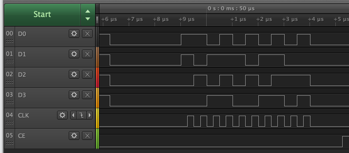
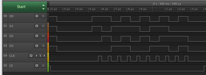
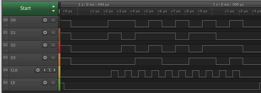
Here is my write timing at 4MHz so my logic analyzer can capture it. It's showing address + data phase to write a byte in nibble mode PSRAM. Reads start out the same and then switch to input mode later. Turns out the rising clock actually is 1/4 into the bit, not 3/4 in sysclk/4 mode as I had initially thought.
Sysclk/2 (clock is centered)
Sysclk/3 (rising clock is 2/3 into bit)
Sysclk/4 (rising clock is 1/4 into bit).


Comments
Any 1 bit PSRAM mode is going to be really slow as the address needs to be single bit serially clocked as well as the data. We're already talking 80 P2 clocks for transferring a single byte, and 16 P2 clocks for each additional byte after that. Not sure what it gains apart from a 4 pin minimum count vs 6 pins, which provides ~4x the performance with those 2 extra pins. A really pin constrained environment might find some use I guess. Not for emulators or much video (though 4bpp VGA resolution could possibly use it). Maybe you could share some of its pins with SPI SD or other flash devices...
No, never got around to that.
Got the delay test working with sysclk/2 writes and sysclk/3 reads with Rayman's 24MB board in 4 bit mode. The acceptable delay range widens with this change which is good.
Will try the 96MB board next.
PSRAM 4 bit memory read delay test over frequency, ESC exits Enter the base pin number for your PSRAM (0,4,8...52) [40]: 48 Enter the chip enable pin number for your PSRAM [57]: 53 Enter the clock pin number for your PSRAM [56]: 52 Enter an additional CE/CLK P2 pin to drive high (0-55), or a higher value to exit [56]: 54 Enter an additional CE/CLK P2 pin to drive high (0-55), or a higher value to exit [56]: 55 Enter an additional CE/CLK P2 pin to drive high (0-55), or a higher value to exit [56]: 56 Enter a starting frequency to test in MHz (100-350) : [100] 300 Enter the ending frequency to test in MHz (300-350) : [300] 350 Enter 1 to use the automatic delay value only, or 0 to test over the delay range : [0] 0 Enter 1 to display the first error encountered, or 0 to not display error details : [0] 0 Testing P2 from 300000000 - 350000000 Hz Successful data reads from 100 block transfers of 8192 random bytes Frequency Delay 3 4 5 6 7 8 9 10 11 12 13 14 300000000 (11) 0% 0% 0% 0% 0% 100% 100% 100% 100% 100% 0% 0% 301000000 (11) 0% 0% 0% 0% 0% 100% 100% 100% 100% 100% 0% 0% 302000000 (11) 0% 0% 0% 0% 0% 100% 100% 100% 100% 100% 0% 0% 303000000 (11) 0% 0% 0% 0% 0% 100% 100% 100% 100% 100% 0% 0% 304000000 (11) 0% 0% 0% 0% 0% 100% 100% 100% 100% 100% 0% 0% 305000000 (11) 0% 0% 0% 0% 0% 100% 100% 100% 100% 100% 0% 0% 306000000 (11) 0% 0% 0% 0% 0% 100% 100% 100% 100% 100% 0% 0% 307000000 (11) 0% 0% 0% 0% 0% 100% 100% 100% 100% 100% 0% 0% 308000000 (11) 0% 0% 0% 0% 0% 100% 100% 100% 100% 100% 0% 0% 309000000 (11) 0% 0% 0% 0% 0% 100% 100% 100% 100% 100% 0% 0% 310000000 (11) 0% 0% 0% 0% 0% 100% 100% 100% 100% 100% 0% 0% 311000000 (11) 0% 0% 0% 0% 0% 100% 100% 100% 100% 100% 0% 0% 312000000 (11) 0% 0% 0% 0% 0% 100% 100% 100% 100% 100% 0% 0% 313000000 (11) 0% 0% 0% 0% 0% 100% 100% 100% 100% 100% 0% 0% 314000000 (11) 0% 0% 0% 0% 0% 100% 100% 100% 100% 100% 0% 0% 315000000 (11) 0% 0% 0% 0% 0% 100% 100% 100% 100% 100% 0% 0% 316000000 (11) 0% 0% 0% 0% 0% 100% 100% 100% 100% 100% 0% 0% 317000000 (11) 0% 0% 0% 0% 0% 100% 100% 100% 100% 100% 0% 0% 318000000 (11) 0% 0% 0% 0% 0% 100% 100% 100% 100% 100% 0% 0% 319000000 (11) 0% 0% 0% 0% 0% 100% 100% 100% 100% 100% 0% 0% 320000000 (11) 0% 0% 0% 0% 0% 100% 100% 100% 100% 100% 0% 0% 321000000 (11) 0% 0% 0% 0% 0% 100% 100% 100% 100% 100% 0% 0% 322000000 (11) 0% 0% 0% 0% 0% 100% 100% 100% 100% 100% 99% 0% 323000000 (11) 0% 0% 0% 0% 0% 99% 100% 100% 100% 100% 100% 0% 324000000 (11) 0% 0% 0% 0% 0% 74% 100% 100% 100% 100% 100% 0% 325000000 (11) 0% 0% 0% 0% 0% 16% 100% 100% 100% 100% 100% 0% 326000000 (11) 0% 0% 0% 0% 0% 0% 100% 100% 100% 100% 100% 0% 327000000 (11) 0% 0% 0% 0% 0% 0% 100% 100% 100% 100% 100% 0% 328000000 (11) 0% 0% 0% 0% 0% 0% 100% 100% 100% 100% 100% 0% 329000000 (11) 0% 0% 0% 0% 0% 0% 100% 100% 100% 100% 100% 0% 330000000 (11) 0% 0% 0% 0% 0% 0% 100% 100% 100% 100% 100% 0% 331000000 (11) 0% 0% 0% 0% 0% 0% 100% 100% 100% 100% 100% 0% 332000000 (11) 0% 0% 0% 0% 0% 0% 100% 100% 100% 100% 100% 0% 333000000 (11) 0% 0% 0% 0% 0% 0% 100% 100% 100% 100% 100% 0% 334000000 (11) 0% 0% 0% 0% 0% 0% 100% 100% 100% 100% 100% 0% 335000000 (11) 0% 0% 0% 0% 0% 0% 100% 100% 100% 100% 100% 0% 336000000 (11) 0% 0% 0% 0% 0% 0% 100% 100% 100% 100% 100% 0% 337000000 (11) 0% 0% 0% 0% 0% 0% 100% 100% 100% 100% 100% 0% 338000000 (11) 0% 0% 0% 0% 0% 0% 100% 100% 100% 100% 100% 0% 339000000 (11) 0% 0% 0% 0% 0% 0% 100% 100% 100% 100% 100% 0% 340000000 (12) 0% 0% 0% 0% 0% 0% 100% 100% 100% 100% 100% 0% 341000000 (12) 0% 0% 0% 0% 0% 0% 100% 100% 100% 100% 100% 0% 342000000 (12) 0% 0% 0% 0% 0% 0% 100% 100% 100% 100% 100% 0% 343000000 (12) 0% 0% 0% 0% 0% 0% 100% 100% 100% 100% 100% 0% 344000000 (12) 0% 0% 0% 0% 0% 0% 100% 100% 100% 100% 100% 0% 345000000 (12) 0% 0% 0% 0% 0% 0% 97% 100% 100% 100% 100% 0% 346000000 (12) 0% 0% 0% 0% 0% 0% 93% 100% 100% 100% 100% 0% 347000000 (12) 0% 0% 0% 0% 0% 0% 59% 100% 100% 100% 100% 0% 348000000 (12) 0% 0% 0% 0% 0% 0% 1% 100% 100% 100% 100% 0% 349000000 (12) 0% 0% 0% 0% 0% 0% 0% 100% 100% 100% 100% 0% 350000000 (12) 0% 0% 0% 0% 0% 0% 0% 100% 100% 100% 100% 0%Here's one of the previously worst performing devices on the 96MB board running with sysclk/3 reads (in 4 bit mode -still need to test with 8 bits using both devices). Run up to 350MHz.
Enter the base pin number for your PSRAM (0,4,8...52) [32]: 32
Enter the chip enable pin number for your PSRAM [42]: 45
Enter the clock pin number for your PSRAM [40]: 40
Enter an additional CE/CLK P2 pin to drive high (0-55), or a higher value to exit [56]: 42
Enter an additional CE/CLK P2 pin to drive high (0-55), or a higher value to exit [56]: 43
Enter an additional CE/CLK P2 pin to drive high (0-55), or a higher value to exit [56]: 44
Enter an additional CE/CLK P2 pin to drive high (0-55), or a higher value to exit [56]: 46
Enter an additional CE/CLK P2 pin to drive high (0-55), or a higher value to exit [56]: 47
Enter an additional CE/CLK P2 pin to drive high (0-55), or a higher value to exit [56]: 56
Enter a starting frequency to test in MHz (100-350) : [300] 320
Enter the ending frequency to test in MHz (320-350) : [350] 350
Enter 1 to use the automatic delay value only, or 0 to test over the delay range : [0] 0
Enter 1 to display the first error encountered, or 0 to not display error details : [0] 0
Testing P2 from 320000000 - 350000000 Hz

                        Successful data reads from 100 block transfers of 8192 random bytes
Frequency      Delay    3       4       5       6       7       8       9       10      11      12      13      14
320000000        (11)   0%      0%      0%      0%      0%      0%      0%      100%    100%    100%    100%    0%
321000000        (11)   0%      0%      0%      0%      0%      0%      0%      100%    100%    100%    100%    0%
322000000        (11)   0%      0%      0%      0%      0%      0%      0%      100%    100%    100%    100%    0%
323000000        (11)   0%      0%      0%      0%      0%      0%      0%      96%     100%    100%    100%    0%
324000000        (11)   0%      0%      0%      0%      0%      0%      0%      78%     100%    100%    100%    0%
325000000        (11)   0%      0%      0%      0%      0%      0%      0%      41%     100%    100%    100%    0%
326000000        (11)   0%      0%      0%      0%      0%      0%      0%      1%      100%    100%    100%    0%
327000000        (11)   0%      0%      0%      0%      0%      0%      0%      0%      100%    100%    100%    0%
328000000        (11)   0%      0%      0%      0%      0%      0%      0%      0%      100%    100%    100%    0%
329000000        (11)   0%      0%      0%      0%      0%      0%      0%      0%      100%    100%    100%    0%
330000000        (11)   0%      0%      0%      0%      0%      0%      0%      0%      100%    100%    100%    0%
331000000        (11)   0%      0%      0%      0%      0%      0%      0%      0%      100%    100%    100%    0%
332000000        (11)   0%      0%      0%      0%      0%      0%      0%      0%      100%    100%    100%    0%
333000000        (11)   0%      0%      0%      0%      0%      0%      0%      0%      100%    100%    100%    0%
334000000        (11)   0%      0%      0%      0%      0%      0%      0%      0%      100%    100%    100%    0%
335000000        (11)   0%      0%      0%      0%      0%      0%      0%      0%      100%    100%    100%    0%
336000000        (11)   0%      0%      0%      0%      0%      0%      0%      0%      100%    100%    100%    0%
337000000        (11)   0%      0%      0%      0%      0%      0%      0%      0%      100%    100%    100%    0%
338000000        (11)   0%      0%      0%      0%      0%      0%      0%      0%      95%     100%    100%    0%
339000000        (11)   0%      0%      0%      0%      0%      0%      0%      0%      84%     100%    100%    0%
340000000        (12)   0%      0%      0%      0%      0%      0%      0%      0%      60%     100%    100%    0%
341000000        (12)   0%      0%      0%      0%      0%      0%      0%      0%      7%      100%    100%    0%
342000000        (12)   0%      0%      0%      0%      0%      0%      0%      0%      0%      100%    100%    0%
343000000        (12)   0%      0%      0%      0%      0%      0%      0%      0%      0%      100%    100%    0%
344000000        (12)   0%      0%      0%      0%      0%      0%      0%      0%      0%      100%    100%    0%
345000000        (12)   0%      0%      0%      0%      0%      0%      0%      0%      0%      100%    100%    0%
346000000        (12)   0%      0%      0%      0%      0%      0%      0%      0%      0%      100%    100%    0%
347000000        (12)   0%      0%      0%      0%      0%      0%      0%      0%      0%      100%    100%    0%
348000000        (12)   0%      0%      0%      0%      0%      0%      0%      0%      0%      99%     100%    0%
349000000        (12)   0%      0%      0%      0%      0%      0%      0%      0%      0%      34%     100%    0%
350000000        (12)   0%      0%      0%      0%      0%      0%      0%      0%      0%      0%      100%    0%
And here's its pair that makes up the 8 bits:
PSRAM 4 bit memory read delay test over frequency, ESC exits
Enter the base pin number for your PSRAM (0,4,8...52) [40]: 36
Enter the chip enable pin number for your PSRAM [57]: 45
Enter the clock pin number for your PSRAM [56]: 41
Enter an additional CE/CLK P2 pin to drive high (0-55), or a higher value to exit [56]: 42
Enter an additional CE/CLK P2 pin to drive high (0-55), or a higher value to exit [56]: 43
Enter an additional CE/CLK P2 pin to drive high (0-55), or a higher value to exit [56]: 44
Enter an additional CE/CLK P2 pin to drive high (0-55), or a higher value to exit [56]: 46
Enter an additional CE/CLK P2 pin to drive high (0-55), or a higher value to exit [56]: 47
Enter an additional CE/CLK P2 pin to drive high (0-55), or a higher value to exit [56]: 56
Enter a starting frequency to test in MHz (100-350) : [100] 320
Enter the ending frequency to test in MHz (320-350) : [320] 350
Enter 1 to use the automatic delay value only, or 0 to test over the delay range : [0] 0
Enter 1 to display the first error encountered, or 0 to not display error details : [0] 0
Testing P2 from 320000000 - 350000000 Hz

                        Successful data reads from 100 block transfers of 8192 random bytes
Frequency      Delay    3       4       5       6       7       8       9       10      11      12      13      14
320000000        (11)   0%      0%      0%      0%      0%      0%      0%      0%      100%    100%    100%    0%
321000000        (11)   0%      0%      0%      0%      0%      0%      0%      0%      100%    100%    100%    0%
322000000        (11)   0%      0%      0%      0%      0%      0%      0%      0%      100%    100%    100%    0%
323000000        (11)   0%      0%      0%      0%      0%      0%      0%      0%      100%    100%    100%    0%
324000000        (11)   0%      0%      0%      0%      0%      0%      0%      0%      100%    100%    100%    0%
325000000        (11)   0%      0%      0%      0%      0%      0%      0%      0%      100%    100%    100%    0%
326000000        (11)   0%      0%      0%      0%      0%      0%      0%      0%      100%    100%    100%    0%
327000000        (11)   0%      0%      0%      0%      0%      0%      0%      0%      100%    100%    100%    0%
328000000        (11)   0%      0%      0%      0%      0%      0%      0%      0%      100%    100%    100%    0%
329000000        (11)   0%      0%      0%      0%      0%      0%      0%      0%      99%     100%    100%    0%
330000000        (11)   0%      0%      0%      0%      0%      0%      0%      0%      99%     100%    100%    0%
331000000        (11)   0%      0%      0%      0%      0%      0%      0%      0%      76%     100%    100%    0%
332000000        (11)   0%      0%      0%      0%      0%      0%      0%      0%      21%     100%    100%    0%
333000000        (11)   0%      0%      0%      0%      0%      0%      0%      0%      0%      100%    100%    0%
334000000        (11)   0%      0%      0%      0%      0%      0%      0%      0%      0%      100%    100%    0%
335000000        (11)   0%      0%      0%      0%      0%      0%      0%      0%      0%      100%    100%    0%
336000000        (11)   0%      0%      0%      0%      0%      0%      0%      0%      0%      100%    100%    0%
337000000        (11)   0%      0%      0%      0%      0%      0%      0%      0%      0%      100%    100%    0%
338000000        (11)   0%      0%      0%      0%      0%      0%      0%      0%      0%      100%    100%    0%
339000000        (11)   0%      0%      0%      0%      0%      0%      0%      0%      0%      100%    100%    0%
340000000        (12)   0%      0%      0%      0%      0%      0%      0%      0%      0%      100%    100%    0%
341000000        (12)   0%      0%      0%      0%      0%      0%      0%      0%      0%      100%    100%    0%
342000000        (12)   0%      0%      0%      0%      0%      0%      0%      0%      0%      100%    100%    0%
343000000        (12)   0%      0%      0%      0%      0%      0%      0%      0%      0%      100%    100%    0%
344000000        (12)   0%      0%      0%      0%      0%      0%      0%      0%      0%      100%    100%    0%
345000000        (12)   0%      0%      0%      0%      0%      0%      0%      0%      0%      100%    100%    0%
346000000        (12)   0%      0%      0%      0%      0%      0%      0%      0%      0%      100%    100%    0%
347000000        (12)   0%      0%      0%      0%      0%      0%      0%      0%      0%      100%    100%    0%
348000000        (12)   0%      0%      0%      0%      0%      0%      0%      0%      0%      100%    100%    0%
349000000        (12)   0%      0%      0%      0%      0%      0%      0%      0%      0%      100%    100%    0%
350000000        (12)   0%      0%      0%      0%      0%      0%      0%      0%      0%      100%    100%    0%
This is what it got before at sysclk/2 read rate (in a combined 8 bit mode, so not a perfect comparison, but still)
So based on the above results @Wuerfel_21 , there may now be some scope to get NeoYume running faster with the 96MB board with sysclk/3 read rates instead of sysclk/4. You can keep my driver as is writing at sysclk/2 and just need to change your own read code a little. I think you can theoretically shave 13+n P2 clocks off the read latency for each burst transfer of n bytes this way in an 8 bit PSRAM setup with sysclk/3 reads vs sysclk/4 which should help. It does cost two more instructions though (if you can do something in the waitx time like a mergeb) so I guess it's 9+n in reality.
The key is to use clock pulse mode instead of transition mode, and you need to setup the clock phase correctly at the beginning of the read request. My code does this, yours will be slightly different due to how you do your tri-state waits and delays but the two wxpins and the waitx delay at the beginning are needed and the clock count is now half of what it was before. You might be able to do something useful instead of the waitx perhaps but you'll probably need two instructions between both wxpins to be sure it transitions by 1 clock before resetting the duty cycle. divideby3 = $20003, nco_slower = $2aaaaaab
wxpin #1, #PSRAM_CLK_PIN ' adjust timing to one P2 clock per update for precise adjustment drvl #PSRAM_CE_PIN drvl #PSRAM_DATA_PINS wxpin divideby3, #PSRAM_CLK_PIN waitx #0 xinit ximm8, pattern wypin #15, #PSRAM_CLK_PIN ' enough clocks for address phase, delay and 1 byte transfer xcont #0, #0 xcont #6, #0 fltl #PSRAM_DATA_PINS wrpin registered, #PSRAM_DATA_PINS setq nco_fast xcont #DELAY, #0 xcont #6, #0 setq nco_slower xcont xread2, #0 ' read data waitxfi ' wait until streamer is done wrpin registered, #PSRAM_DATA_PINS drvh #PSRAM_CE_PINGot NeoYume working with sysclk/3.
Here were the changes I made...based on my (older) version of this emulator. Run a diff between the two files to see what I did so you can update your own code for the 96MB board, Ada.
Also the magic required numbers in config.spin2 with this change were PSRAM_WAIT = 5, PSRAM_DELAY = 14, although other nearby DELAY values might also work too at sysclk/3 rates. PSRAM_WAIT=5 makes more sense to me because there are 5 actual PSRAM clock cycles needed after the 8 nibble address transfer before the read data begins. It's multiplied by either 2 or 3 for sysclk/2 or sysclk/3 rates because the streamer has switched back to nco_fast (sysclk/1) at this point so you need to scale it back to real P2 clocks. Then a delay of 14 P2 clock cycles is added before reading begins to account for the total pipeline and board delays encounted by the read operation. It all works out.
UPDATE: PSRAM_DELAY = 15 and PSRAM_DELAY=16 also work, so you might pick the middle one of 15. The values of 13 and 17 didn't work for me.
UPDATE2: not sure if I am just imagining it but a couple of times the input control felt a tad laggy perhaps in a couple of places with lots of screen activity when running sysclk/3. Nothing visibly noticeable though.
Sounds good, will have to look into it later
Looks like it fits in the 16 bit driver as well, and even leaving me with one LUTRAM long to spare. Luxury! I initially had two LUTRAM longs free, and if I used the optimization I found previously for pik33 locked request list feature, that actually frees another 2. The sysclk/3 change itself takes 4 instructions but also saves one elsewhere in the clock calculation. So it looks like we are good to put this feature into all PSRAM drivers. It also needs one more COGRAM long for the duty cycle storage but we had three spare anyway. The other driver variants have more space free and are okay.
This new feature is useful because it allows people to not overclock the PSRAM, or choose to operate at a slower but working speed if the PSRAM output drive's slew rate is not fast enough due to too much load with multiple banks for example. I'm expecting some good things with Rayman's 96MB board now at very high P2 clock speeds allowing it to continue to operate in those situations with only a moderate performance hit.
I think I will keep sysclk/2 the default for PSRAM unless overridden, in which case operating at sysclk/3 or sysclk/4 can be selected at startup. Even though it violates the duty cycle requirement I sort of expect sysclk/3 to be safe to use. I imagine this 50% duty cycle restriction mainly applies when you are clocking at sysclk/2, so there is enough high and low time on the clock signal for sample/hold purposes. Because we are essentially just doubling the low time, and keeping the high time the same, I'm thinking we should be good. If there was some type of PLL or something like that inside the device that was timed off each edge to generate some internal clock signal, I'd be more worried about changing the duty cycle to 33:66%, but in this case it appears to work. But people can always fall back to sysclk/4 if they have to, at the expense of some additional performance loss.
PLLs can be "picky" as of reference input duty cycles when they differ too much from the ideal 50/50, but only when the input clock is used as is (without prescalling), because it tends to "foul" their phase comparators.
Also it would be very hard (in the sense of needed hardware structures) to keep with input references whose periods could be otherwise schrunked, stretched or totally stopped.
There are no PLLs at PSRams that deppends-on their clock input pin(s), whichever bit-"flavours" they can have (4, 8, 16...). This includes all the Xccela-Consortium-tagged versions, and all HyperBus derivative devices.
In relation to their input clock waveforms, for each kind of working cycle (read or write), there is an active border to be followed/observed. The internal state machine relies on an interlocking process, in order to deal with all aspects of defined/required data-transfer operations.
The absence of any externally-accessible DQS/DM or RWDS signals doesn't mean they don't exist; they're just embodied, and used as an integral part of the request/acknowledge mechanism.
When present (Hypers and Xccelas), their "data mask" function is just a "free reward"; kind off a "useful remanent" from the time when "protecting" some part of the data-words against overwriting was of utmost importance.
I've been bashing away at doing an educational version of this, ie: Using the streamer for performance databus ops. And doing it in a way that shows any desired setting is possible. But damn, it ain't easy. The dance of aligning the timings of multiple pins at different clock ratios and speeds and specific alignments forces hand coded numbers all over the place. There is such a thing as too tight.
PS: I did find a simpler solution that eliminates the hand coded lead-in timing by swapping out the SPI clock's Pulse Mode smartpin for PWM Mode and instead rely on CE going low for start of the SPI transaction. But, because of timing limitations around when CE can go low, sysclock/2 becomes inflexible. (Data pins have to stay registered for perfect timing).
At any rate, it takes advantage of the fact that extraneous clock pulses are ignored prior to CE low and also ignored after the command is completed.
... dirh #PSRAM_CLK_PIN ' start SPI clock pulses, PWM smartpin waitx #1 + CLK_REGD - DAT_REGD xinit ##M_CA4, paddr ' tx Command and Address (byte granular address) drvl #PSRAM_CE_PIN ' tightly follows streamer to signal CA start ...Hi @evahn
Ain't there any risks for command termination to be misinterpreted by PSram, in the sense one must ensure CE# going high well within CLK = "Low"-period?
I've managed to come up with a sequence that mostly now works for sysclk/2 sysclk/3 and sysclk/4 and have now added it to my 4,8,16 bit PSRAM drivers. The only downside is that (only) in the sysclk/4 case the clock is not fully centered in the middle of the sent bit (it's at 3/4 I think) but given that is running much slower and we have more headroom there on writes, I'm not too concerned about that limitation. For the reads you can center the clock with the optimal delay setting.
Here's the main sequence (including my skipf stuff for bytes/words/long/bursts and optional registered data pin controls). I've also used a method from Ada's code now to wait for tri-stating, doesn't save any cycles but it's probably a little neater to read/understand than my old way. You do need a 2 clock delay slot after the second wxpin before the xinit, which I've used for one of the address setup instructions (in this case a movbyts). You do get a few spots in the sequence where you can run other instructions while the streamer is being operated. I've used them to compute / restore the clock delays. The value of clkdelay is different for sysclk/2, /3 and /4, but can be determined in advance and remains fixed at a given clock divisor for the streamer. I also have my own fine delay on top of this which is a per bank setting.
wxpin #1, clkpin 'increase clock update rate drvl cspin 'activate chip select drvl datapins 'enable data bus wxpin clkduty, clkpin 'resync clock output movbyts cmdaddr, #%%0123 'reverse bytes in address to match bus order xinit ximm8, cmdaddr 'stream out command+address wypin clks, clkpin 'start clock output add clkdelay, delay 'add configurable fine input delay setq xfreq1 'reconfigure with single cycle xfreq (sysclk/1) xcont clkdelay, #0 'streamer transfers during bus turnaround delay and read latency sub clkdelay, delay 'restore for next time waitxmt 'wait until first command has completed before tri-stating fltl datapins 'safe to float the data bus, address has been sent by now wrpin regdatabus, datapins 'setup data bus inputs as registered or not for read timing control if_z skipf #%0100100 'special skip case for read-modify-write(RWM) 'Bursts Bytes Words Longs RMW setq xfreq2 ' a b c d e xcont xrecvdata, #0 ' a b c d e transfer data as nibbles call resume ' a b c d | waitxfi ' a b c d e wait for streaming to finish wrpin registered, datapins ' a b c d e restore data pins for next transfer _ret_ drvh cspin ' a b c d | de-assert chip select and returnNo problem there. Commands are finished long before CE rises again.
You're missing a needed lead-in timing alignment. A WAITX (with handcrafted delay) should be placed just in front of the XINIT. I have different values for each sysclock ratio.
Here's what I was using for a while:
                dirh    #PSRAM_CLK_PIN      ' start smartpin cycling
                waitx   #(DELAY_SMART + CLK_REGD - DAT_REGD) +// CLK_RATIO  ' smartpin cycle alignment - clock ratio dependent
                xinit   ##M_CA1, paddr      ' tx Command and Address (byte granular)
                wypin   len, #PSRAM_CLK_PIN ' SPI clocks for CA phase, and data phase
With these hand crafted values:
' DELAY_SMART = 0 ' tuned for sysclock/2 SPI clock DELAY_SMART = 0 ' tuned for sysclock/3 SPI clock ' DELAY_SMART = 3 ' tuned for sysclock/4 SPI clockHowever, I gave up on that approach because it proved problematic, not dissimilar to the PWM approach above, where one of the four sysclock/2 combinations could not be aligned. EDIT: The combination with data pins unregistered, clock pin registered.
PS: I'm back to pursuing the wordier approach of using XINIT then SETQ+XCONT for initiating CA phase in place of the lead-in WAITX. It still needs the handcrafted alignment encoded in the first XINIT but it's not timing limited like the other approaches.
xinit ##M_LEADIN, #0 ' lead-in timing, at sysclock/1, includes smartpin cycle alignment setq ##($8000_0000 +/ CLK_RATIO) ' streamer transfer ratio xcont ##M_CA1, paddr ' tx Command and Address (byte granular address) dirh #PSRAM_CLK_PIN ' start smartpin cycling wypin len, #PSRAM_CLK_PIN ' SPI clocks for CA phase, and data phaseStrange, mainly because PSRams do rely on the raising edge of CLK, in order to properlly identify the command termination itself, but the timing diagrams seen to be a little misleading, to say the least;
(data from APS6404L-3SQR devices datasheet, page 10)
As for Write to be considered as properlly terminated, CE# "Can Be" de-asserted (High-going) as short as 3nS after the "Rising Edge" of the Last CLK, which effectivelly "clocks" (sic) the last data item, towards PSRam inner "guts";
As for Read to be considered as properlly terminated, CE# "Can Be" de-asserted (High-going) as short as 3nS after the "Rising Edge" of the Last CLK, which effectivelly "signs" the completion of the Read operation, but the data transfer of the last nibble towards the I/O buffers. will depend on the forthcoming "Low-going Edge" of that same CLK pulse, so there's an observation/warning at the same item/page: "For a memory controller to correctly latch the last piece of data prior to read termination, it is recommended to provide a longer CE# hold time (tCHD > tACLK+tCLK) for a sufficient data window".
Its kind of a "Brain Salad Surgery", perpetraded by some drunk surgeon, and lacking all "nice sound effects"...
To be "Crystal Clear" (and in the sake of any minor sanity, still resting inside my own brain): Command Termination not only means the end of current operation (in progress), but also means PSRam's internal state machine will not try to continue the ongoing operation, "internally", e.g., understanding a burst as crossing actual row address limits.
Ouch...
Huh, maybe combine both: Use the flexible streamer approach plus the PWM as clock approach to eliminate the hand crafted alignment ... something like:
xinit ##M_LEADIN, #0 ' lead-in timing, at sysclock/1 setq ##($8000_0000 +/ CLK_RATIO) ' streamer transfer ratio xcont ##M_CA4, paddr ' tx Command and Address (byte granular address) dirh #PSRAM_CLK_PIN ' start SPI clock pulses, PWM smartpin"as short as 3nS" is the operative words there. You can happily make it much longer and not care about the end-of-command timing.
You're absolutely right, provided the last CLK-signal "completely-stops" after its forthcoming "Low Going" edge.
Any reasonable "rebound" (in the sense of total voltage excursion), either due to an undamppened reflexion (or even excessive ground bounce) would put such "command termination"-interpretation at risk, which could, in turn, cause some malfunction, be it due to "incomplete (or even totally skipped) self-refresh cycles, or beyound "normal" inter-command "minimum innactivity" (CE# tCPH >= 18nS) limits.
The clock doesn't actually need to stop (at any time). It is ignored once the command is completed. No further commands will be accepted until CE cycles high and back low. One command per CE cycle.
If the actual drivers are currently lefting "Page Boundary Crossing" enabled, that statement does not apply, since the PSRam will be ever prepared for a "possible and eventual" RBX-event (that means it'll do each and every "internal housekeeping" needed), as if the commands would really continue.
Sure, it'll only affects Read ad Write operations at the main memory array. but that's enough to cause havoc.
Oh, you might have a point, I'd not thought about writing data to the RAM. I've mostly been concerned with the fixed length commands in my testing.
Yes, using PWM as clock would then need precise CE timing for command termination on RAM block writes. That might be possible given that writes are currently pretty uncomplicated.
I've been "eating" those datasheets, without any good spice (for them to taste any better) almost since the first 4-bitters appeared, too long ago (SRAMSUN, et al.)...
(my connection went "weird", so I'm complementing, based on your latest edition)
Reads would also kind of "need" them, because those tiny monsters seem to have two fifos; that's the reason for needing a CLK "slow-down" (84MHz, at the datasheet, which would translate to ~12nS of "extra" low-time between the last CLK full-cycle from the first "block", and the first High-going CLK pulse of the next one, but them, up to 2048 consecutive bytes can be I/O'lled (sic) with only one Command/Address sequence (and, sure, would need propper calculations, so as to don't causing havoc with self-refresh timing).
O.S. the "extra" ~12nS would be the time needed to MUX the secondary Fifo, as it could be the primary-one, then the primary would became the secondary, and so on...
This is kind of new territory too. Previous approaches were all using exact number of clock pulses so CE termination wasn't thought about at all.
No need, because my movbyts performs the 2 clock cycle wait function. It would be a wasted WAIT #0 otherwise, which is what I started with, so I can put a useful instruction there to save a couple of clocks. This works for sysclk/2 and sysclk/3 with both registered data and clock pins (which is what I'm using in my driver at this point in the address phase). Sysclk/4 does slightly offset the clock phase by an extra P2 clock though as I mentioned, and I'm unconcerned about that. You can select unregistered data in the lsb of my provisioned bank delay, but that occurs after tri-stating. There is no unregistered clock selection for this driver (like we had for the experimental sysclk/1 HyperRAM stuff). That can fix the sysclk/4 but introduces more selection logic and cycles to switch on/off dynamically.
Hmm, not looking simple. WAITXFI is ~4..6 sysclocks too late to use for bashing CE on time.
Pure luck - that those fell that way. EDIT: I guess at sysclock/4 it's leaning to your advantage because 3 of the 4 alignments will work.
Here is my write timing at 4MHz so my logic analyzer can capture it. It's showing address + data phase to write a byte in nibble mode PSRAM. Reads start out the same and then switch to input mode later. Turns out the rising clock actually is 1/4 into the bit, not 3/4 in sysclk/4 mode as I had initially thought.
Sysclk/2 (clock is centered)
Sysclk/3 (rising clock is 2/3 into bit)
Sysclk/4 (rising clock is 1/4 into bit).
Here's the test code I used for the above:
CON _clkfreq = 4000000 BAUD = 115200 PSRAM_DATA_PINS = 8 + (3<<6) PSRAM_CLK_PIN = 12 PSRAM_CE_PIN = 13 SYSCLK_DIV1 = $80000000 SYSCLK_DIV2 = $40000000 SYSCLK_DIV3 = $2AAAAAAB SYSCLK_DIV4 = $20000000 OBJ uart:"SmartSerial" f:"ers_fmt" PUB main() asm wrpin #0, #PSRAM_CE_PIN drvh #PSRAM_CE_PIN fltl #PSRAM_CLK_PIN wrpin ##%100_000_000_01_00100_0, #PSRAM_CLK_PIN ' pulse mode registered clock pin wxpin #1, #PSRAM_CLK_PIN drvl #PSRAM_CLK_PIN wrpin ##%100_000_000_00_00000_0, #PSRAM_DATA_PINS ' registered data bus pins endasm write_test(2) write_test(3) write_test(4) repeat PUB write_test(divisor) | divider, nco, wrclks, cmdaddr, ximm8, xsendimm, hubdata case divisor 2: divider := $10002 nco := SYSCLK_DIV2 3: divider := $20003 nco := SYSCLK_DIV3 4: divider := $20004 nco := SYSCLK_DIV4 other: return asm setxfrq nco endasm wrclks := 8+2 ' byte write as 2 nibbles after 8 nibble address phase cmdaddr := $af25af35 ' address+cmd pattern ximm8 := $6091_0008 ' 8 nibble immediate transfers xsendimm := $6090_0002 ' 2 nibble immediate transfers hubdata := $d4 ' data pattern repeat 1 asm wxpin #1, #PSRAM_CLK_PIN ' adjust timing to one P2 clock per update for fast adjustment drvl #PSRAM_CE_PIN ' activate chip select drvl #PSRAM_DATA_PINS ' enable the data bus wxpin divider, #PSRAM_CLK_PIN ' restart pulse mode divider waitx #0 ' delay xinit ximm8, cmdaddr ' send 8 nibbles of address and command via LUT translation wypin wrclks, #PSRAM_CLK_PIN ' start memory clock output xcont xsendimm, hubdata ' send immediate data as nibbles waitxfi ' wait for streamer to end fltl #PSRAM_DATA_PINS ' tri-state DATA bus drvh #PSRAM_CE_PIN ' de-assert chip select endasm waitms(500)Ah, that's only one of the four combinations of clock/data pin registration.