

Ethernet PHY Accessory board
 ManAtWork
Posts: 2,367
ManAtWork
Posts: 2,367
in Propeller 2
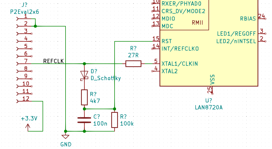
With great help from the community I make some good progess with the low-level Ethernet driver. So I think it's time to think about an accessory board with RMII interface. I'm starting a new thread about the hardware, here, so it doesn't get lost in the long discussion about software, timings etc.
The part count is so low that I think it doesn't make sense to make an adaptor board for the Waveshare eval board, instead. Maybe, Parallax is interested in producing and selling the board. If not I'll put it in the public domain or create a sharable project at some board house such as OSHPark.
I've attached my first draft for the schematic. The differences to my current prototyping setup with the Waveshare board are:
- low cost 25MHz crystal instead of 50MHz oscillator
- REF_CLK output mode (better margins for setup/hold times)
- correct polarity of the LEDs
- TXD0 and MDIO share the same pin so everything fits on a single 12-pin header
- RXER is not used
pdf
51K
Comments
Would it make sense to add a 24AA02E48 to have a unique MAC address onboard? I think it could be tied to the MDC and TXD1 pins. If we make sure that no start conditions are generated while talking to the PHY via SMI the I2C chip should keep quiet. MDIO is connected to TXD0 so that SMI and I2C communication can be handled separately. And MDC stays low during RMII packet transmission which uses TXEN to signal valid data.
I like the idea of a single 12 pin breakout for P2 once you've proven the clock will work. Having a proper unique MAC address available is the way to go.
Yeah I think MDC and TXD1 would be possible to use with MDC=I2C SCL and TXD1 as I2C SDA (and TXD0 for MDIO). You can hold potentially hold MDC low all the time while in normal Ethernet RMII mode, clock it with TXD0 changing for SMI, or clock it for I2C SCL with TXD0 high to keep SMI inactive, and transition TXD1 for the I2C data. You'd only need to use I2C once at the start anyway so it doesn't need to be continually accessed and doesn't ever really have to interleave with either SMI or RMII. I think this should work out with suitable driver pin control applied.
REFCLK as an input
I personally don't like the idea to generate the RMII REFCLK with the P2. I have some doubts that this would work reliably for any frequency other than 200MHz because that's the only one which is a multiple with a power of two factor in the valid range. Every odd NCO divider value will produce either non-50% duty cycle or a phase glitch once per wrap-around. Ethernet is quite sensitive about clock stability so I'd vote for a local crystal clock source. It also provides more margin for the data setup and hold times.
However, the idea to make the release of /RST dependant on the presence of the clock is cool. I don't think it's absolutely necessary, though. All standard features like changing the speed or full duplex ability and restarting auto-negotiation can also be done via the SMI interface. Only if the PHY is in an undefined state or lock-up then /RST is the only way out. But that shouldn't happen. With the accessory board we get rid of all the jumper wires, traces are really short and everything should work reliable.
Ok, I'll add the 24AA02E48. I'll make some boards and test them. If they work reliably and all signals look good I'll keep the crystal and REFCLK output mode. If we find any problem we can change it by adding some piggypack resistors and a diode like in Evanh's suggestion (and do a layout respin for the final production version, of course).
Is there a preferred form factor for accessory boards? The minimum size I could squeeze it should be around 45x20mm.
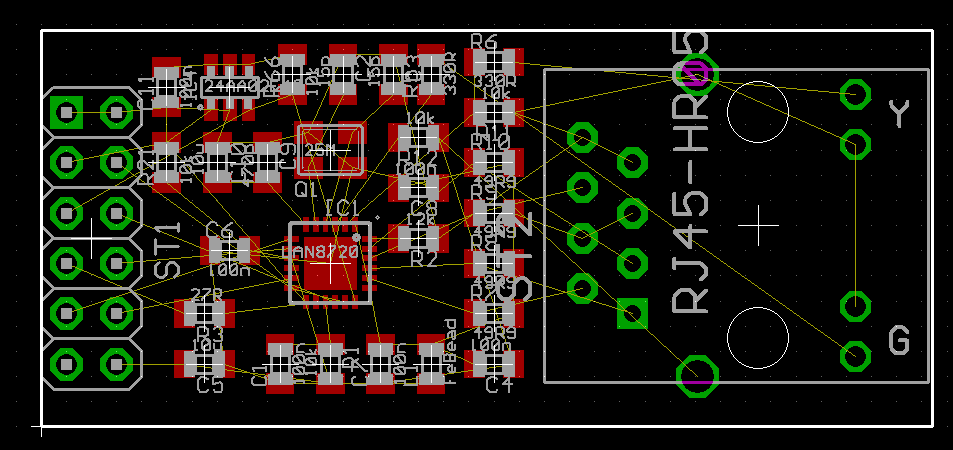
That's ideal. 20 mm wide is the narrow form single header. No limit on length. 33 mm wide is the wide form single header.
If you have the board space and with solder jumpers in appropriate positions, maybe you can have a board option to test the external clock out mode from the P2? Although if the streamer is to be also be used then you'd need to setup data pins on even+odd pairs I think, as your current mapping starts them off from an odd pin instead.
Many of the other Parallax P2 breakout boards are 40mm long. If you squeeze the LED resistors under the RJ45, maybe you could shave your board down to that size, to make the connectors of other breakout boards line up...(I know, that's probably going a bit OCD on it, but if it's ever inside a chassis it could be helpful to have them the same length to line up connectors on panel edges etc). Some of the 49 ohm ones might also fit there. Not sure about EMI/RF impacts of doing that though. LED stuff should be fine I suspect, no high speed signals there.
I guess 100 MHz would work also, when not using the full bandwidth. Maybe also 250 and 150. You would have to rewrite the software for streamer mode though and i don't see any reason for that. The idea was to be able to choose any P2 frequency freely.
If the Eval Board was to be targetted for a deployment solution you'd want to do it as a piggy back, with the expansion stacked on top and plugged into multiple headers.
Ok, you're right. I've rearranged the port pins so that RX0/1 and TX0/1 are on even/odd pin pairs. I also try to include Evanh's schottky diode trick for /RST and jumpers for REFCLK input vs output mode. But I try to avoid placing parts on the bottom side, at least those for the regular version (crystal + REFCLK out mode). That would require selective soldering or gluing+wave soldering. 40mm length could be possible when switching to 0604 or 0402 resistors ans caps. But I'll go for the 0805 sizes for now as I have them all in stock.
Edit: added updated schematic
An added pull-down resistor is needed on RST when using the diode.
Double check the individual polarities of that dual diode. They're often packaged nose-to-nose or tail-to-tail.
Thanks, Evanh. Updated schematic:
Yeah it's a pity the header connector is on the top side, otherwise all parts could probably be soldered on the same (bottom) side. The RJ45 connector is a through hole part so it needs to be mounted through the board and soldered underneath, unless you reverse mount from below and solder on the top layer? Which way around will it go?
Ah, the original Parallax accessory boards have top mounted but bottom insert pin sockets for the P2 ports. That needs even more space. Ok, I could mount RJ45 connector and pin header on the bottom side and all SMD parts on the top. But this would require hand soldering, even too hard for selective soldering if squeezed into 20x40mm.
Squashing it to 40 mm long is silly unless you are trying to save a few cents on PCB costs. Even if the Eval board goes in a box, it should never have the accessory connectors exposed to operators.
With 20x45mm, the RJ45 connector on top and the pin socket mounted on the bottom (hand soldered) everything fits nicely. All SMD components for the standard versions are on the top side and all jumpers and optional parts for the modified version are on the bottom.
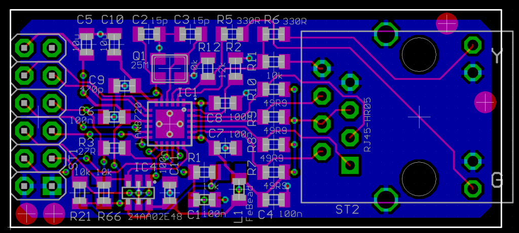
The fiducials hardly fit in but for the production version we have to make a panel with multiple boards and holding tabs, anyway.
A possible concern in mounting the pin socket on the bottom side, is the possibility of its SMT solder pads being subjected to extra flexural/torsional stresses during insertion/operation, since at the "normal position" (top side), the pcb unmetalized vias can provide some "guidance", while shortenning the "unguided-pin-lenghts", at the same time.
But this can be proved to be just a misconception of mine...
It is likely that someone might want to use the P2 dev board or some 3rd party board together with expansion modules, put them in a custom housing and sell it as a product. then if the Rj45 jack stood out a bit and there were mounting holes on the board, it could be made accessible easily. otherwise one would have to use some kind of patch cable/patch panel to bring out the ethernet connector.
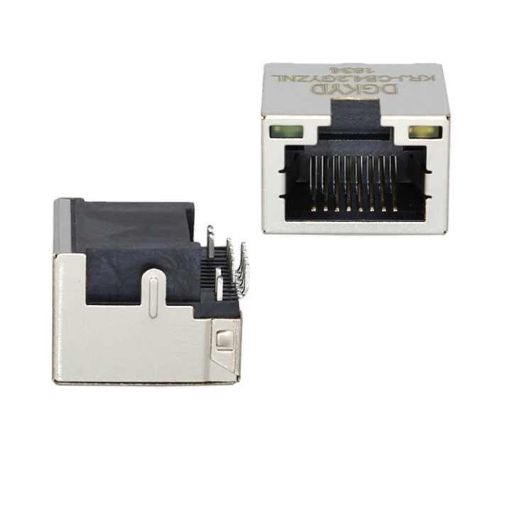
There exist Ethernet connectors with built-in LEDs. Might save a few parts there. S.
Yes, but that's only a concern with SMT headers. They would be mounted on top, anyway. My through-hole headers for the prototype boards are rock solid. If you brake them it's your fault.
If 0603 or 0402 Rs and Cs were used and the board had 5mm overhanging on the Eval board side maybe it would be possible to fit everything on the common 40x20 size.
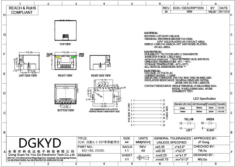
I know. Look at the picture in post #17. "Y" and "G" labels on the right side.")
Would that suggest you were going to actually produce these boards or am I making things up ?
I'll make 3 or 5 boards for testing but I won't do mass production. Hopefully, Parallax can make them if they want to. LCSC has all parts in stock so we could also order them readily assembled in China if not.
I found this connector on an ST Dev board. I'm not sure if it does help when this could be soldered from the same side as the socket header")
Not just only silly, the PCB layout need to meet requirements for proper isolation. Just one of the first google examples:
https://resources.altium.com/p/gigabit-ethernet-101-basics-implementation
"In addition to these specified restrictions, the discrete magnetics layout may also need special care. A separate ground plane should be created to provide improved ESD and EMI/EMC immunity, and it should be strictly separated from all other planes by at least 2 mm (See Figure 23)."
Ramon,
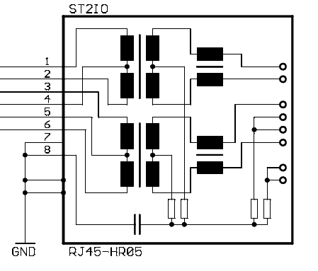
ManAtWork is using one of those RJ45 sockets that has the coupling transformers all built in:
My opinion is that two different grounds (signal ground plane and chassis ground plane) must exist, separated at least 2 mm. The signal ground plane should never enter the RJ45 connector area (as the picture above). And the chassis ground plane (or "shield GND" on the previous post picture) should just cover the connector front and solder pin area.
There could be other opinions: https://www.signalintegrityjournal.com/articles/1808-ethernet-connectors-and-routing-above-ground-planes
The explanation quoted above applies to RJ45 connectors with external magnetics (transformers). They have a primary side (labeled RX/TX) which belongs to the PHY and the system ground plane. The secondary side is connected to the cable side and belongs to the shield ground plane. No signal of each ground domain should overlap the ground plane of the opposite domain, of course. The two ground planes have to be isolated and coupled only via a high voltage capacitor or a surge supressor.
RJ45 sockets with integrated magnetics are a completely different story. Primary and secondary side of the transformers are shielded by one common sheet metal case. The high voltage capacitor is also integrated. You can't do much about it but have to trust that the manufacturer did everything right about isolation and shielding.
Connecting the cable/shield ground to the system ground in this case should theoretically be avoided but is common practice at least on many evaluation boards and consumer electronics. Even most "professional" PC equipment doesn't differentiate between cable ground and signal ground (of the motherboard). I do have seperate ground planes on my industrial boards. This improves EMI/noise immunity and ESD protection a bit. For prototyping and breadboard setups I wouldn't care much. You have so many "flying probes" and jumper wires that everything else will fail before the Ethernet connection does.
Good news: The driver software is basically working. At least I can receive from and transmit to my PC. There needs to be some cleanup and further testing but I think no major show-stoppers are to be expected. So I'm going to order five or ten PCBs on monday. I'd like to keep two so there will be 3 to 8 available for anyone who is interested in testing or software development. At this early stage the board is not yet usable for real applications because a protocol stack like TCP/IP is still to be implemented. It's also quite likely that we have to do changes to the schematics or a layout re-spin. So unless you are willing to contribute to the project please stay patient.
Underneath the connector is no ground plane at all")
Ok, nobody seems to be interested. Ken didn't even answer my mail. So there won't be an "official" Ethernet accessory board from Parallax. I stop this project and use the RMII based interface for my own applications, only.