Full-chip integration at On Semi
 cgracey
Posts: 14,300
in Propeller 2
I've been at ON Semiconductor in Pocatello all week to help get Prop2 through some hoops.
This is actually the same plant that built the chips for the Atari video game consoles in the late 1970s. Of course, the fab has gone through many renovations and expansions since then.
I brought the layout here after making many edits to it after Treehouse quit working on it.
Nathan, the layout guy here, had our layout into his tool on Monday morning and had that thing whipped into shape in a few minutes. He's like a shark with layout, pushing it through design-rule checks and netlist comparisons, fixing things, iterating again, and getting it clean. He is extremely fast and can buffer a whole slew of edits in his head, getting them done maybe 50x faster than I could. He could have been a vicious lawyer:

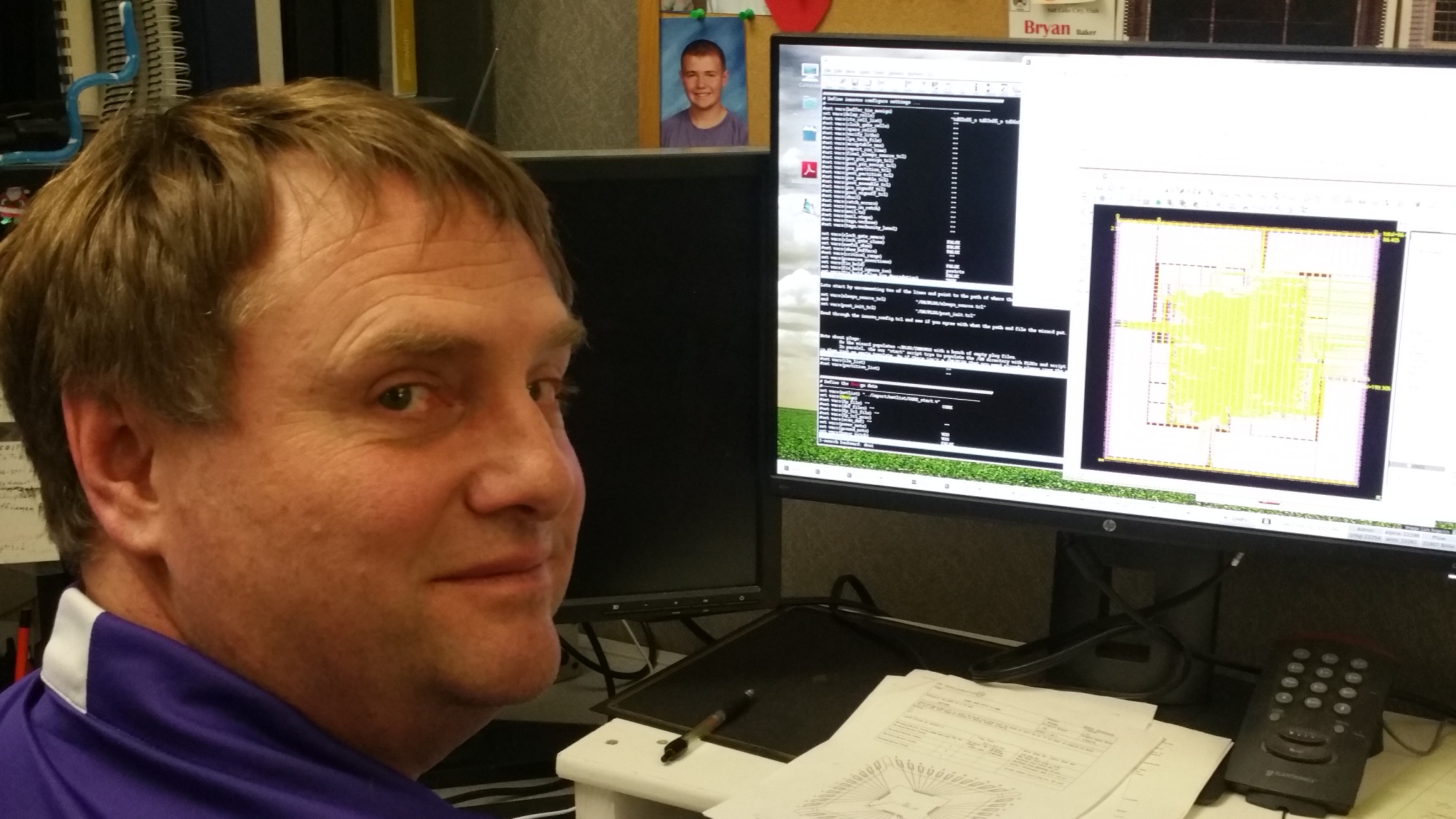
Bryan is the guy who is running the Innovus tool which places all the cell instances and routes them together, automatically moving them around, as needed. Nathan's work is done, so now Bryan is the critical path:
Here is a closer pic of a preliminary place-and-route run:
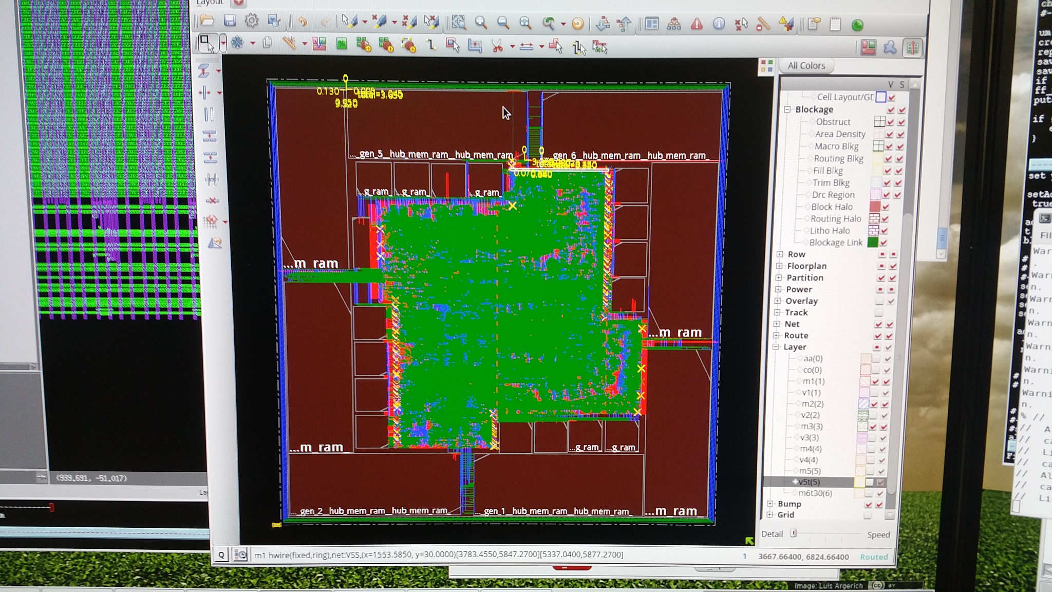
You can see the big hub RAMs laid against the interior of the cell area, while the cog register RAMs and lookup RAMs are nestled into the interior side of the hub RAMs. This process is iterative until the final metrics and scripts are established.
This is actually the same plant that built the chips for the Atari video game consoles in the late 1970s. Of course, the fab has gone through many renovations and expansions since then.
I brought the layout here after making many edits to it after Treehouse quit working on it.
Nathan, the layout guy here, had our layout into his tool on Monday morning and had that thing whipped into shape in a few minutes. He's like a shark with layout, pushing it through design-rule checks and netlist comparisons, fixing things, iterating again, and getting it clean. He is extremely fast and can buffer a whole slew of edits in his head, getting them done maybe 50x faster than I could. He could have been a vicious lawyer:

Bryan is the guy who is running the Innovus tool which places all the cell instances and routes them together, automatically moving them around, as needed. Nathan's work is done, so now Bryan is the critical path:

Here is a closer pic of a preliminary place-and-route run:

You can see the big hub RAMs laid against the interior of the cell area, while the cog register RAMs and lookup RAMs are nestled into the interior side of the hub RAMs. This process is iterative until the final metrics and scripts are established.


Comments
Thanks to Nathan the shark, and place'n'route Bryan! (n Bryan Baker junior egging Dad on)
Thanks for the update Chip!
This design looks a lot less scary than that more organic looking one did.
With the trial P & R, do you get any MHz values reported yet ? How does OnSemi expect those MHz to converge on the target ?
Way to go Nathan and Bryan!
Yes, cog RAM and LUT RAM instances are the same memory cell.
No timing, yet. We have a problem, though. That P&R run that Bryan was doing had only 334k cells in it. Before, we had been dealing with 724k cells. The trouble was that the last set of files I had sent to Wendy (who does the synthesis at ON in Texas) had the #define not commented out which gets rid of the CORDIC. I don't think the CORDIC takes half the logic, by a long shot, though. Wendy is recompiling now and doing a new synthesis run which should be back up to 724k cells. It's looking like it will NOT fit, though we knew that it would be okay, earlier. Something's amiss that we will figure out shortly.
Is the ROM at about 10 o'clock? What are the red blocks and spikes?
Ouch, that's quite a jump(drop) in cell count. Hopefully there are no other #defines lurking in there !
The trip went great. Things are on a super trajectory now. They just need fine-tune the place-and-route and meet timing.
Since they are letting the Innovus tool assemble the pad ring, with it inserting filler power-ring cells, as needed, between pads, they'll be able to let the overall die size float to whatever it can optimally be, considering the internal cell-area requirement. This also means that by making a Verilog change, which would, in turn, affect the Innovus scripts, we could make any of the following without repeating the base effort:
- 16 cogs, 1MB hub, 64 I/Os, TQFP-100
- 4 cogs, 256KB hub, 32 I/Os, TQFP-52
- 2 cogs, 128KB hub, 32 I/Os, TQFP-52
- 1 cog, 64KB hub, 16 I/Os, TQFP-28
It shouldn't cost much more to build any of those variants. We just need to prove the base design.
We've got really nice pads. I hope it all works properly. It should.
Interesting. I had expected the outer PAD Ring to be quite locked down dimensionally.
Wont that die be too large for the package ? - or did you mean not in 180nm ?
TQFP-28 does not really exit, but TQFP-32 is quite common popular, 7mm sq with 0,8mm pitch
TQFP-52 is not common in USA, but Renesas offer MCU's in this, 10mm sq body, 0.65mm pitch
I see one MCU in 52-VQFN (7x7), which looks to sneak 4 diagonal corner pins into a 48-QFN package. (0.5mm pitch)
More common is a TQFP48, (& QFN48) with 7mm body, but die size may dictate what fits inside that, next common step from that is 64 LQFP 10mm x 10mm, 0.5mm pitch
SiLabs QFN parts are cheaper than TQFP versions, so I guess that stems from a package price difference.
Thanks Chip
Pretty sure the P2 in layout is 512kB
A TQFP100 with 1MB and 16 cogs would be pure joy
A TQFP52 with 256KB and 4cogs would be a nice sibling Ng too.
BTW I have no problems with the TQFP52 package.
LQFP 100 + exposed pad = 101 pins at the land pattern
14mm x 20mm body profile, 16mm x 22mm tip-to-tip dimensions
1.4mm body thickness
0.65 pin-to-pin pitch (Attention please, easy hand-soldering fans!!)
2 x 21 pins (14mm sides) (my guesses only; can be 20 pins)
2 x 29 pins (20mm sides) (my guesses only; can be 30 pins)
I'm yet to find any info about the inward available dimensions, that will define maximum silicon area.
https://c44f5d406df450f4a66b-1b94a87d576253d9446df0a9ca62e142.ssl.cf2.rackcdn.com/2018/02/Amkor_LineCard.pdf
I really like the sound of 512K for the Propeller! 16 Cogs and 1MB hub sounds even better. I can't begin to imagine what people will concoct with that much room and/or 16 cogs.
So glad to see the Propeller 2 at this stage.
So... What's limiting you from starting with the 16 cog/1MB?
Surely the larger die wouldnt add much to the ultimate cost of the end chip, and would be a seriously better chip than a 512KB 8 Cog chip ???
The larger die area would bump the package size significantly ?
Is there a FPGA that can emulate such a design ?
Next stops after 14x14 package look to be 14x20 (128 pins) or 20x20 (144 pins) 24x24 (176 pins) 28x28 (208 pins)
Given P2 currently has only 64io, those pin counts are rather unbalanced ?
The reason we didn't start with 16 cogs was package size and even greater power dissipation.
Would 16 cogs and 1 MB of Hub be worth a speed reduction from 160 MHz to 120 MHz?
Mike