

Sunnyside the Pico compatible P2 module
 SaucySoliton
Posts: 587
SaucySoliton
Posts: 587
Note: This post contains info about the old FLiP compatible concept. Look down to see the current Pico compatible designs.
Great for breadboard use or as an upgrade for designs using FLiP or a DIP 40 P1. Will be slightly wider than a FLiP or DIP 40.
USB-C connector with data pins P62, P63. Reset signal on USB SBU pins. For now it would work with special prop plug with type C output. In the future we could have a native USB bootloader. I think an FTDI chip would fit on there if desired.
At the other end maybe a 4 pin JST for I2C. (QWIIC) If the PCB is 0.8 to 1mm thick then an edge connector for an HDMI cable is possible. Or another USB-C connector so the Sunnyside and Prop-Plug-C are the same board.
Power supply would generate the 1.8v from the 3.3v since the P1 only receives 3.3v. If used in place of a FLiP it would accept 5-9v from the appropriate pin.
Not routed yet, but I think it's possible with 4 layers.
Comments
Interesting idea. Wonder if all the Parallax style 0402 caps could fit on there. Maybe...
Nice!
A usb-serial chip will make it complete and a SD card slot will enhance it greatly.
Neat idea. If you have room somewhere eg. down near your potential HDMI connector (full size or micro?), a spare SOP8 footprint for devices with 6 free IO available could be useful for anyone interested in soldering in some optional additional flash or PSRAM device etc, as such spare memory is always useful for video, or for emulation applications. Certainly PCB real estate will start to get tight once you start routing and adding such features however.
Maybe the KISS board gives some inspiration
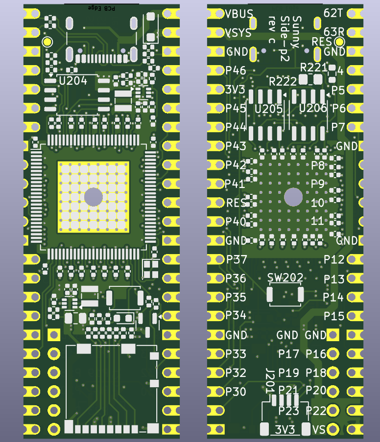
3 pins longer than a Pi Pico
16 MB PSRAM optional
2 EVAL connectors
USB-C upstream and downstream allows the same product to be used as a prog plug (with type C) or target board.
Interesting sacrifice of some through hole pins at the closest side to the P2 to keep the width in check.
How much total IO do you intend to bring out? Looks like it could do something similar to P2-EC32MB ~40 GPIO pins or so, maybe a few more.
This is my take at a low cost P2 board.
Mostly Pi Pico compatible pinout. It's a bit longer.
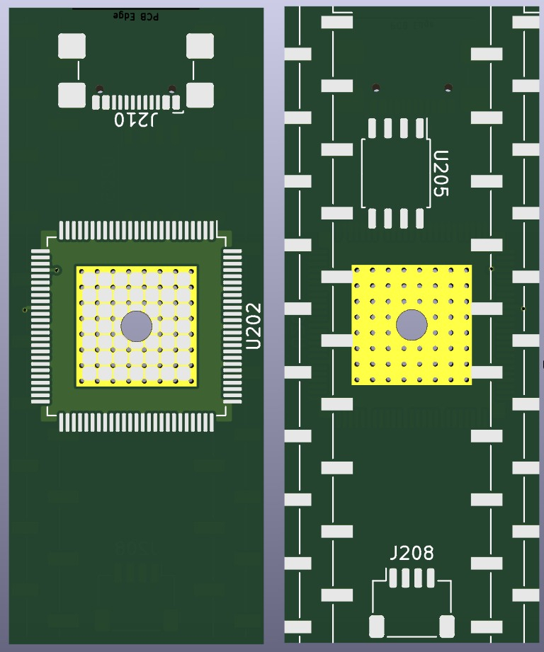
Single sided pick and place (except PSRAM. Although overclocking might not be great with capacitors on 2 edges only.)
Breadboard compatible .1" through hole headers. I think it would be possible to bend some of the top pins to connect to the castellated edge and get all of the pins.
Uses the P2 internal crystal oscillator to save a few cents and lower standby power.
USB-C connector for programming. I think a native USB bootloader is possible. Until that happens, those pins can be used for the usual serial programming.
A second USB-C connector to program another board or connect to USB devices.
4 layer board without via-in-pad.
7 pins lost due to lack of space to route them. (Pins 0-3, 38-39, 47)
10 pins PSRAM (48-57)
4 pins flash (58-61)
41 total GPIO, including P62-63. 29 on a breadboard, 33 castellated. (Pico has 26)
2 pins dedicated to QWIIC connector. (32-33)
2 EVAL connectors, 1 with 5v power
Pins starting with B are the inside columns.
I pivoted towards Pico compatible instead of FLiP compatible. But I still really like the Sunnyside name.
Hi
That looks good!
For my projects an SD card holder is much more useful than a second USB though....
Christof
Looks useful, nice that it's breadboard-able. Given the proximity you might be able to add extra PropPlug holes with tweaks along top edge in case you need some initial programming without custom USB-C cable availability and before USB capable bootloader is installed into the flash.
Still keep it simple, not every feature and /or pin out is needed on the P2 FLIP module. My concern / problem has been the fan out /_PCB real estate used for all the P2 i/o pins for my PCB layout application. In other words, use header connections on the "top side" of the P2 FLIP module for things like a Key pad, LCD display module, VGA or HDMI video, fitted with a ribbon cable arrangement. Consider 8 or 16 pin groupings for this.
Nice to have, but not necessary: uSD card socket, 16 MB SPI Flash, only one USB-C connection, no JST connectors, Internal VDD Power Supply(s)
Remember, it is up to the PCB layout and engineer /programmer, to make the best use of any uP and features, and adapt as necessary
Gave up one EVAL header to fit the micro SD card. 4 bit interface.
Prop plug header could be attached to the board with some creative soldering.
So can this already be bought somewhere?
No. I haven't even built a prototype. I'm willing to make commercially if there is demand and you can even help customize it.
Most importantly, are you looking for a flip compatible or pico compatible?
I like the pico one better because it has more pins. But compatibility with flip or pico isn’t needed in my case as this would replace a stm32 board, the dip form factor is the important thing for me.
Is .1" inch pitch important? The through hole pins on the pico style are .7" apart. The castellated edges are not on a .1" grid.
Do you want the one with 2 EVAL headers (more GPIO) or the one with the microSD?
Do you want 16MB PSRAM? With a smaller flash chip it's possible the PSRAM could fit on top. I designed it so it to be a usable basic board with the top side parts only. I chose the large PSRAM chips so they could be added later.
There are a few things I'm not quite sure about. The bypass capacitors on the top are only on 2 sides instead of all 4 like the Edge. I added additional capacitors on the back side in case they are needed. I won't know if they are really needed until I build some of these. In practice it will depend on the clock frequency. Even 2 layer boards are fine at 250MHz. 340MHz might need a well designed 6 layer board. The boards I've shown here are low cost 4 layer boards.
The 6 small castellated rings, they might be too small for reliable castellation.
It's a native USB interface which will need a USB bootloader that does not currently exist. There is code for a USB serial device. Or a prop plug that outputs to a USB-C connector. It will be possible to program it using the DIP pins.
How many of these do you want?
Any info you don't want post here, like the last one, send a PM.
Oops didn’t realise the pitch wasn’t 0.1”- I would absolutely need that. Breadboard friendliness is essential in my case.
A prop plug interface is needed ihmo, I don’t much like the custom usb loader. Optional 16 mb Psram is enough for me, good idea to use the larger ones so they can be added later. Personally, I don’t need usb connection or sdcard on board, I’d rather have a prop plug header and as much io ports as possible. I wouldn’t mind if the board was a little bit wider (or even longer) to accommodate more through hole pins. My ideal board would even have the prop plug header brought out to the dip headers, but I guess there wouldn’t be much interest in that)
I don't believe that RPi has a board that supports the extra I/O of the RP2350B.
This one can be ordered fully assembled from JLCPCB. Last I checked, they also showed availability of the P2.
Would be perfect if your board was available in a similar footprint.
Two separate breadboards side by side or slice one?
So basically "as many breadboard friendly pins as possible." The Pi Pico is fully breadboard compatible. The castellated edges are .1" pitch, but .826" center to center. Because the P2 is such a big chip I had to remove some of the through hole pins. I think I can get those 6 castellated pins to the breadboard with some creative bending and soldering of the pin headers.
I will assume you would like the P2 facing down so the silkscreen faces up.
Should I remove P4 to fit the prop plug connection on the dip pins? I already put a reset pad there so a prop plug header could be creatively soldered there.
I could extend it by 4 pins and break out the microSD pins. Would you like that?
Do you use any boards with the 12 pin EVAL headers?
Breadboard compatibility is very important for me too.
That red board looks like the spacing between rows is 1.0". Not really usable on small breadboards. Well, I guess you could use half the pins.
Found this limousine of a board. https://shop.pimoroni.com/products/pimoroni-pico-lipo-2-xl-w?variant=55447911006587 Not sure why it has castellated edges since it won't sit flat.
Guess you could make a cutout in the base PCB.")
or, maybe that it looks consistent within their range, or just pretty
Ok,
If the P2 faces downward fitting a heat sink would be difficult, don’t know how much of a problem that actually is and having a usable silk screen with pin numbers would be nice too - difficult one.
Extending the board to make room for extra pins sounds great to me, I mean anything up to 63 pins will fit on a full size breadboard;-) The “P2-stretch”.
I don’t have any eval boards, I just use breadboard breakout boards for everything, as those will work with other platforms as well.
Heat-sinking the back side is far more effective. That's where the thermal pad is located and soldered to the PCB. James has even provided a decent cavity to solder a thermocouple right on the Prop2 thermal pad.
PS: On that note, James, I'd recommend the PCB space inside the ring of backside ceramic capacitors be left without solder-mask so it can be a good thermal contact surface for a correctly sized heat-sink shoulder.
Then still need to solve best way of holding such a heat-sink to the PCB though. That, I don't have any good ideas about.
All the P2 boards I've built have the soldermask removed on the backside of the P2. I forgot why I added soldermask on this one. Anyway, back to the old footprint that I got from the forum.
It’s unfortunate that P0-P3 are not on the headers, is there no way to get those? Having P0-P31 on the headers and a way to plug in a prop plug (even with a tiny connector) would be great.
Cool.
I was going to say no way for P0-P3. But, I thought that even if I can't get more pins that P0-P7 would be more useful than P4-P11 since we use groups of 8.
Board will grow to 30 pins per side. The castellated edge on the left will become through holes and move out to be .8" on center from the right side through holes.
I did a test route for P0-P12 and it was necessary to interleave pins to make it work. Some other pins are interleaved because they are part of an EVAL header. The inside pins of the EVAL header are assigned wherever they can fit.
Excellent ideas, P0-P31 are there, and even an eval header - and good to have the through hole pins on the left now!
P31 is the SD power control. That is routed out because I thought it could be useful to have a switched power output. The MOSFET could be jumpered to use P31 as IO. Or if capacitance must be minimized it can be jumpered to P34.
The QWIIC connector uses P32-33 which are not routed to DIP headers. Pins 37-39 are tied together. 47 breadboard IO pins plus 2 on the QWIIC connector.