Hello @evanh , I have tried the changes you suggested but still i am not able to see data on pins.
I am using Below code. i can able to see clock pulses getting high low as per code(In 13.5 ns) but not able to see output on PC(Pin 16), PM(Pin 17), PY(Pin 18), AD(Pin 19).
send_mix_Data_asm(int index) { for(int i = 0;i<40;i++) { unsigned char d = hex_t[index][i]; __asm { // allowed to be optimised and hubexec inlined OUTL #6 //CLK = 1 setbyte outa, d, #2 // pins P16..P23 OUTH #6 //CLK = 0 } } }
And when i am using below code, with using loop in PASM2, still there is no output and also garbage data observed on F1(Pin 4) and F2(Pin 5).
I tried to run previous code to check hex_t data is proper or not with _pinwrite(). and i am getting proper output on pins but its taking more time. So can you please suggest what i am doing still wrong in PASM2 code?
void send_mix_Data(int index) { int i = 0; _pinw(ADATA, 0); for (i = 0; i < 40; i++) { _pinw(ADATA, 0); _pinwrite( 12|7<<6, hex_t[index][i]); // write to pins P16, P17, P18,P19
Hex data = 50 Hex data = 20 Hex data = 50 Hex data = 20 Hex data = 50 Hex data = A0 Hex data = 50 Hex data = 20 Hex data = 50 Hex data = 20 Hex data = 50 Hex data = 20 Hex data = 50 Hex data = 20 Hex data = 50 Hex data = 20 Hex data = 50 Hex data = 20 Hex data = 50 Hex data = 20 Hex data = 50 Hex data = 20 Hex data = 50 Hex data = 20 Hex data = 50 Hex data = 20 Hex data = 50 Hex data = 20 Hex data = D0 Hex data = 20 Hex data = 50 Hex data = 20 Hex data = 50 Hex data = 20 Hex data = 50 Hex data = 20 Hex data = 50 Hex data = 20 Hex data = 50 Hex data = 20 Hex data = 50 Hex data = 20 Hex data = 50 Hex data = 20 Hex data = 50 Hex data = 20 Hex data = D0 Hex data = 20 Hex data = 50 Hex data = 20 Hex data = 50 Hex data = 20 Hex data = 50 Hex data = 20 Hex data = 50 Hex data = 20 Hex data = 50 Hex data = 20 Hex data = 50 Hex data = 20 Hex data = 50 Hex data = 20 Hex data = 50 Hex data = 20 Hex data = 50 Hex data = 20 Hex data = 50 Hex data = 20 Hex data = 50 Hex data = 20 Hex data = 50 Hex data = 20 Hex data = 50 Hex data = 20 Hex data = 50 Hex data = 20 Hex data = 50 Hex data = 20 Hex data = 50 Hex data = 20 Hex data = 50 Hex data = 20 Hex data = 50 Hex data = 20 Hex data = 50 Hex data = A0 Hex data = D0 Hex data = 20 Hex data = 50 Hex data = 20 Hex data = 50
Oh, you also need the DIR bits set at some point earlier. All pins are bidirectional. It was in the original demo code but I didn't make the detail clear, sorry.
I used _pinl( GROUP<<3|7<<6 ); to drive the outputs in the demo. And then _pinf( GROUP<<3|7<<6 ); to release them after.
Hello @evanh i have already defined the pins as output on starting of the code.
Also i have used your suggested _pinl() and _pinf(). But issue was different.
I found the issue. i am using bits 7, 6, 5 and 4 (from 1 byte data) for pins 16, 17,18 and 19 and i have to use bits(0,1,2,3). I have changed my hex manipulation code. and now i am getting data. But still i am getting noise on other signal lines with this code.
send_mix_Data_asm2(int index) { for(int i = 0;i<40;i++) { data_hex[i] = hex_t[index][i]; } unsigned char* haddr = data_hex; int val; int len = 40; int pingroup = 2; __asm { .loop OUTH #6 //CLK = 1 rdbyte val, haddr // access hubRAM, intervals of 24 ticks add haddr, #1 setbyte outa, val, #2 // pins P16..P23 OUTL #6 //CLK = 0 djnz len, #.loop } }
Please check attached signals. Why i am getting noise on signal lines especially with above code?
Also, above code taking 81 ns , can i make it more fast?
@chintan_joshi said:
Also, above code taking 81 ns , can i make it more fast?
Well, there is the smartpins for single pin functions. We've been using them a lot as a clock pin for SPI, I2C, SD and the likes. Each physical pin has one associated smartpin. They are each a little state machine that can run various pulse gen, counter functions and simple serial, not to mention dithering for the internal DACs and sigma-delta ADC bitstream capture.
So, instead of bit-bashing the clock output, you can concurrently have a smartpin generating a simple square wave for the clock pin.
And such a smartpin can be matched with a streamer to provide impressive bandwidth. Memory is quickly used up. :O
.
EDIT: Working with what's there, the code can be placed in cogRAM instead leaving it in main memory (hubRAM). Add a volatile keyword as per earlier examples.
And, once sitting in cogRAM, replacing the DJNZ loop with a REP loop will knock four ticks off the loop time.
EDIT2: Another one is overclock the chip. The Prop2 can operate over 300 MHz relatively easily. 350 MHz if lightly loaded. My example code has the enums for setting the initial run time frequency. I've selected 4 MHz for diag purposes. Just edit as desired.
@chintan_joshi said:
Please check attached signals. Why i am getting noise on signal lines especially with above code?
Can't tell from the limited info. No idea which traces are which pins. And the source code is incomplete.
One possibility is those spurious traces are just floating pins creating an illusion in the logic capture. An oscilloscope would show the analogue waviness.
@chintan_joshi said:
Also, above code taking 81 ns , can i make it more fast?
Well, there is the smartpins for single pin functions. We've been using them a lot as a clock pin for SPI, I2C, SD and the likes. Each physical pin has one associated smartpin. They are each a little state machine that can run various pulse gen, counter functions and simple serial, not to mention dithering for the internal DACs and sigma-delta ADC bitstream capture.
So, instead of bit-bashing the clock output, you can concurrently have a smartpin generating a simple square wave for the clock pin.
And such a smartpin can be matched with a streamer to provide impressive bandwidth. Memory is quickly used up. :O
.
EDIT: Working with what's there, the code can be placed in cogRAM instead leaving it in main memory (hubRAM). Add a volatile keyword as per earlier examples.
And, once sitting in cogRAM, replacing the DJNZ loop with a REP loop will knock four ticks off the loop time.
EDIT2: Another one is overclock the chip. The Prop2 can operate over 300 MHz relatively easily. 350 MHz if lightly loaded. My example code has the enums for setting the initial run time frequency. I've selected 4 MHz for diag purposes. Just edit as desired.
Hey @evanh i have already changed Clock frequency to 297 MHZ. and logic signals i shared are from 297 MHZ clock frequency setup.
Sorry but can you please guide me about how can i use REP in place of DJNZ?
297 MHz? I've seen that number used around here before ... for video modes. There is a number of LCD panels already in operation by various forum members. You could try Googling for "site:forums.parallax.com" with the interface type or brand of LCD.
I've just verified (for the first time) my example program. The data is being driven onto the pins. The code you've listed from your program shouldn't be a problem.
@evanh said:
I've just verified (for the first time) my example program. The data is being driven onto the pins. The code you've listed from your program shouldn't be a problem.
Yes right, but when i changed djnz to rep then only i am not able to see data on pins. So is there anything we need to change for rep?
I am trying to use DMA example code. But i can see only clock signal lines on Pin 6, Sorry I am new to PASM2 language, how can i change this code to work for Pin 16,17,18,19 (Data pins 16,17,18,19)and 6(Clock pin)? I want to load 40 bit data on Pin 16,17,18,19 with 40 clock pulses, so i have changed len = 40, and changed pgroup to 2.
int len = 40; int pgroup = 2; uint32_t m_nco = M_NCO; uint32_t m_tx = X_RFBYTE_8P_1DAC8 | pgroup<<20 | X_PINS_ON | len; // byte wide transfers from hubRAM, via the FIFO uint32_t ticks = _cnt(); //printf("m_tx = %X RF = %X group = %X X_P = %X \n",m_tx,X_RFBYTE_8P_1DAC8 , pgroup<<20 , X_PINS_ON); //_waitms(1000); __asm volatile { // no optimising and enforces Fcache use - Needed to free up the FIFO rdfast #0, haddr // setup the FIFO to read from hubRAM setxfrq m_nco // set the transfer rate xinit m_tx, #0 // do it! OUTL #6 OUTH #6 waitxfi // wait for transfer to complete before returning back to hubexec, hubexec uses the FIFO }
It seems like DIR is not set in both cases. Might pay to add a pinl() into that just to be sure.
    for(int i = 0;i<40;i++)
    {
        data_hex[i] = hex_t[index][i];
    }
    unsigned char* haddr = data_hex;
    int len = 40;
    int pgroup = 2;
    uint32_t m_nco = M_NCO;
    uint32_t m_tx = X_RFBYTE_8P_1DAC8 | pgroup<<20 | X_PINS_ON | len; // byte wide transfers from hubRAM, via the FIFO
    uint32_t ticks = _cnt();

    //printf("m_tx = %X RF = %X group = %X X_P = %X \n",m_tx,X_RFBYTE_8P_1DAC8 , pgroup<<20 , X_PINS_ON);
    //_waitms(1000);
    pinl( pgroup<<3 | 7<<6 );
    __asm volatile { // no optimising and enforces Fcache use - Needed to free up the FIFO
        rdfast #0, haddr // setup the FIFO to read from hubRAM
        setxfrq m_nco // set the transfer rate
        xinit m_tx, #0 // do it!
        OUTL #6
        OUTH #6
        waitxfi // wait for transfer to complete before returning back to hubexec, hubexec uses the FIFO
    }
@evanh said:
It seems like DIR is not set in both cases. Might pay to add a pinl() into that just to be sure.
  for(int i = 0;i<40;i++)
  {
      data_hex[i] = hex_t[index][i];
  }
  unsigned char* haddr = data_hex;
  int len = 40;
  int pgroup = 2;
  uint32_t m_nco = M_NCO;
  uint32_t m_tx = X_RFBYTE_8P_1DAC8 | pgroup<<20 | X_PINS_ON | len; // byte wide transfers from hubRAM, via the FIFO
  uint32_t ticks = _cnt();

  //printf("m_tx = %X RF = %X group = %X X_P = %X \n",m_tx,X_RFBYTE_8P_1DAC8 , pgroup<<20 , X_PINS_ON);
  //_waitms(1000);
  pinl( pgroup<<3 | 7<<6 );
  __asm volatile { // no optimising and enforces Fcache use - Needed to free up the FIFO
      rdfast #0, haddr // setup the FIFO to read from hubRAM
      setxfrq m_nco // set the transfer rate
      xinit m_tx, #0 // do it!
      OUTL #6
      OUTH #6
      waitxfi // wait for transfer to complete before returning back to hubexec, hubexec uses the FIFO
  }
Yes you are right, _pinl worked. But for single clock pulse data pins are changed 40 times, i want to change each bit with each clock pulse. can you please guide me how can i do that?
Question: Are you wanting DDR or SDR? The fastest a simulated clock can toggle at is one cycle per two sysclocks. If the data is DDR then it can operate at sysclock frequency while the clock output is sysclock/2.
Whereas if SDR is needed then data rate must also be limited to sysclock/2 to match the simulated clock output.
@evanh said:
Question: Are you wanting DDR or SDR? The fastest a simulated clock can toggle at is one cycle per two sysclocks. If the data is DDR then it can operate at sysclock frequency while the clock output is sysclock/2.
Whereas if SDR is needed then data rate must also be limited to sysclock/2 to match the simulated clock output.
Yes i want data to be inserted on shift register on every falling edge of clock signal.
Use my source, as is, without trying to paste it into your code. It performs correctly at sysclock/2, which, if sysclock was to be raised to 297 MHz, would provide data period of 6.7 ns.
        xinit   leadin, #0    // lead-in timing, at sysclock/1
        setq    m_nco2    // streamer transfer rate
        xcont   m_tx, #0    // setup buffered command for tx data
        drvl    datp    // active data pins for tx data
        dirh    clkpin    // start smartpin internally cycling, at SPI clock rate
        wypin   len, clkpin    // produce clocks, starting on second internal cycle
How this block of code works:
Each instruction is two sysclock ticks to execute. No blocking, no hidden prefixes. Instructions are counted out for timing, the code must not be reordered/optimised.
XINIT starts the ball rolling. The length parameter within the M_LEADIN constant defines how many sysclock ticks the streamer will null-cycle for before engaging DMA. This is vital timing to align the start of DMA with the smartpin's simulated clock output.
SETQ is a semi-prefixing instruction. It loads the special Q register but also sets a special flag that modifies behaviour of certain other instructions that execute next. In this case XCONT. The purpose is for adjusting streamer cycle rate from lead-in's sysclock/1 to desired DMA rate, exactly when engaging DMA.
XCONT, in this case, is the streamer command for engaging the DMA'ing. And, as the comments say, XCONT is buffered into the command buffer until the XINIT has completed. The XCONT then seamlessly adjoins to the end of the XINIT.
DRVL is just activating the data pins ready for streamer output - Raising DIR control. It's partly placed here to add a couple sysclocks leeway - Which is helpful for SPI clock mode 0 where data precedes clock.
DIRH is important here for starting up the smartpin for simulated clock output. The smartpin is preconfigured for pulse gen output - P_PULSE mode. This mode internally cycles at its configured rate the moment DIR goes high. Pulses are only outputted on whole cycle boundaries. This means the subsequent WYPIN pulses are aligned with the cycle period starting from this DIRH, not from the WYPIN.
WYPIN does what it says. But everything else prior is all about aligning the data timing to match this simulated clock output.
PS: Extra instructions, eg: DRVL #CS_PIN, may be inserted where the DRVL is. For each extra, add +2 to the length parameter in M_LEADIN.
Avoid use of ##immediates in these instructions. Use register-direct via additional appended data LONGs, eg: leadin long M_LEADIN, instead.
As a C programmer and after looking through this conversation I would have thrown the P2 aside and found something else.
The P2 is not that complicated for just doing simple set 8 data lines and clocking the results without getting into assembly code.
You need to just get something simple to work, version 1 and then move on to making it work better.
Going after the final version and learning what the chip can do at the same time is a recipe for disaster.
I have written many library functions to use with flex prop that can be found here: Flex Prop Libraries
You don't have to use them but there are many examples of writing C code using the P2.
Well, Mike, he did push, repeatedly, for maximum throughput. I certainly didn't present the complex performant method first up. In fact, at times I was starting to think Chintan might lose interest because the options presented weren't fast enough for him.
So far, the application hasn't been revealed. But it's becoming clear it's for a databus of some type. So not unlike the PSRAMs. Which is why I pivoted to that very code. I'm thinking it could be an LCD interface.
Thanks for the link, btw.
PS: I am trying to make the idea of rolling your own DMA solutions more understandable generally. The exercise with the PSRAMs wasn't intended solely for that one application.
Let me add some details here. This is very interesting. I am making inkjet printer controller board. And these CLOCK, and 4 data pins are signal lines for Print Head.
I have to maintain timing(in nano seconds) to drive the print head.
And i am able to drive print head with Nucleo F746ZG micro controller(216 MHZ clock frequency) with required timing.
Only issue with Nucleo Board or any controller is its single core. So i am switching to Propeller 2 board as this board having capability of 8 core.
Basically i have to shift 40 bits data
PDATAC(CYAN color shift register 40 bits)
PDATAM(Magenta color shift register(40 bits))
PDATAY(Yellow color shift register(40 bits))
ADDRESSING Shift register(22 bits)
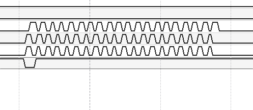
in 40 clock pulses. And all this 3 color bits and addressing bit should shift at a time. as per attached image.
So i made unsigned char HEX array. In which each byte contains each color single bit + Addressing register bits(Total 4 bits ).
In Nucleo board i can able to do this with ( GPIOE->ODR = hex_t[index][i];) instruction. This instruction will write byte on Port E at a time with very high speed(within 15 ns ).
So i am re-developing this code for Propeller 2.
Hope this can help to understand my problem better.
Cool. And only needs 40 transfers at a time? That seems small amount.
Ah, I see the slave is clocked on falling edge. So that's cmode's 1 & 2 rather that 0 and 3. I don't have those combinations in my demo code just yet ...
Okay here's the updated demo code with cmode = 2 (CPOL=1, CPHA=0). I've replaced the CMODE3 flag with the two CPOL/CPHA flags.
@evanh said:
Cool. And only needs 40 transfers at a time? That seems small amount.
Ah, I see the slave is clocked on falling edge. So that's cmode's 1 & 2 rather that 0 and 3. I don't have those combinations in my demo code just yet ...
Okay here's the updated demo code with cmode = 2 (CPOL=1, CPHA=0). I've replaced the CMODE3 flag with the two CPOL/CPHA flags.
I am able to merge your code into mine , Just a little issue.
This is the code i have added in my code. static uint32_t pinout8clk_dma( unsigned pgroup, unsigned clkpin, int index) { for(int i = 0;i<40;i++) { data_hex[i] = hex_t[index][i]; } unsigned char* haddr = data_hex; int val; int len = 40; uint32_t m_tx = X_RFBYTE_8P_1DAC8 | pgroup<<20 | X_PINS_ON | len; // byte wide transfers from hubRAM, via uint32_t datp = pgroup<<3 | 7<<6; uint32_t ticks = _cnt(); __asm volatile { // no optimising and enforces Fcache use - Needed to free up the FIFO rdfast #0, haddr // setup the FIFO to read from hubRAM, non-blocking setxfrq m_nco1 // set sysclock/1 for lead-in timing xinit leadin, #0 // lead-in timing, at sysclock/1 setq m_nco2 // streamer transfer rate xcont m_tx, #0 // setup buffered command for tx data drvl datp // active data pins for tx data dirh clkpin // start smartpin internally cycling, at SPI clock rate wypin len, clkpin // produce clocks, starting on second internal cycle // twiddle thumbs while DMA happens ... waitxfi // wait for transfer to complete before returning back to hubexec, hubexec uses the FIFO dirl clkpin // reset smartpin _ret_ dirl datp // tristate the data bus upon completion leadin long M_LEADIN m_nco2 long M_NCO m_nco1 long 0x8000_0000 } return _cnt() - ticks; }
And calling from Main() like this
_pinf( GROUP<<3 | 7<<6 ); _wrpin( GROUP<<3 | 7<<6, TX_REGD ? P_SYNC_IO : 0 ); // at sysclock/1, data pins should be registered to minimise relative skew _pinf( CLK_PIN ); _wrpin( CLK_PIN, P_PULSE | P_OE | (CLK_REGD ? P_SYNC_IO : 0) | (SPI_CLKMODE3 ? P_INVERT_OUTPUT : 0) ); // clock pins _wxpin( CLK_PIN, CLK_DIV | (CLK_DIV>>1 + (SPI_CLKMODE3 & CLK_DIV))<<16 ); // set period and duty for (int index = 0; index < 20; index++) { //send_mix_Data(index); //__builtin_cogstart(send_mix_Data_asm(index), &stack[1]); //send_mix_Data_asmrep(index); pinout8clk_dma(GROUP, CLK_PIN,index); //LoadFire_thread(); }
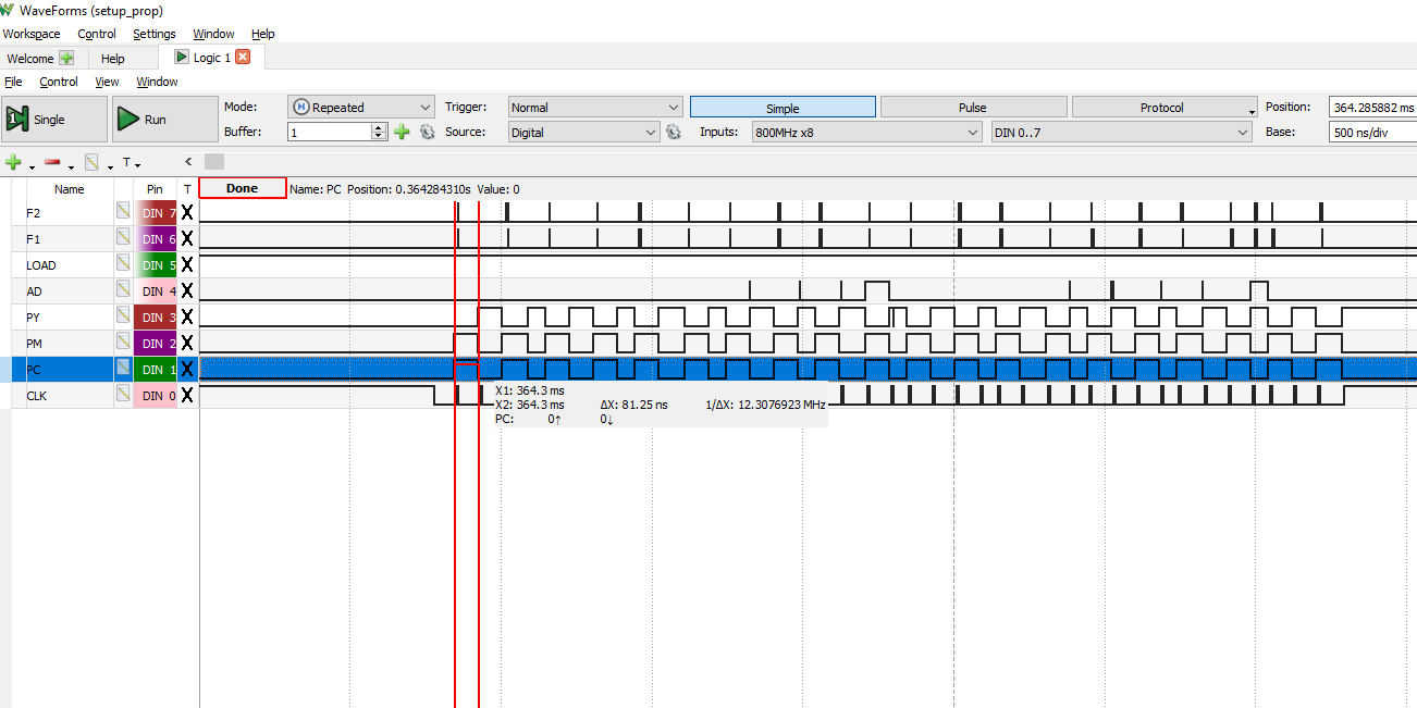
I can able to see CLOCK and other 4 datapins data, but somehow data on pin 19(Addressing shift register) is not as per original data. its changing same like other 3 data lines. Please check below signal trace , specifically AD line.
So do i need to add anything to include to make data available on pin 19 as per HEX data?
I see CLKMODE3 still present. When updated to the CPOL/CPHA code it'll match the printhead datasheet then.
Looking at that image, the captured clock high/low ratio is erratic, but in reality it is consistently even. I'd guess the analyser's sample rate is too low to see the data setup and hold times. Very important to verify such. So, you might want to use a slower sysclock frequency until you are seeing evenly spaced clock on the analyser. Data sequencing can be verified then.
I can't really speak for the data content. Have you tried putting the analyser on my demo code? The demo data content counts up from 1 to 1000.


Comments
Hello @evanh , I have tried the changes you suggested but still i am not able to see data on pins.
I am using Below code. i can able to see clock pulses getting high low as per code(In 13.5 ns) but not able to see output on PC(Pin 16), PM(Pin 17), PY(Pin 18), AD(Pin 19).
send_mix_Data_asm(int index){for(int i = 0;i<40;i++){unsigned char d = hex_t[index][i];__asm {// allowed to be optimised and hubexec inlinedOUTL #6 //CLK = 1setbyte outa, d, #2 // pins P16..P23OUTH #6 //CLK = 0}}}And when i am using below code, with using loop in PASM2, still there is no output and also garbage data observed on F1(Pin 4) and F2(Pin 5).
send_mix_Data_asm2(int index){for(int i = 0;i<40;i++){data_hex[i] = hex_t[index][i];}unsigned char* haddr = data_hex;int val;int len = 40;int pingroup = 2;__asm {.loopOUTH #6 //CLK = 1rdbyte val, haddr // access hubRAM, intervals of 24 ticksadd haddr, #1setbyte outa, val, #2 // pins P16..P23OUTL #6 //CLK = 0djnz len, #.loop}}I tried to run previous code to check hex_t data is proper or not with _pinwrite(). and i am getting proper output on pins but its taking more time. So can you please suggest what i am doing still wrong in PASM2 code?
void send_mix_Data(int index) {int i = 0;_pinw(ADATA, 0);for (i = 0; i < 40; i++) {_pinw(ADATA, 0);_pinwrite( 12|7<<6, hex_t[index][i]); // write to pins P16, P17, P18,P19// Delay_waitx(1);// ClOCk = 0_pinw(CLK, 0);// Delay_waitx(1);// CLOCK = 1_pinw(CLK, 1);_waitx(1);}}My HEX data is something like this
Hex data = 50 Hex data = 20 Hex data = 50 Hex data = 20 Hex data = 50 Hex data = A0 Hex data = 50 Hex data = 20 Hex data = 50 Hex data = 20 Hex data = 50 Hex data = 20 Hex data = 50 Hex data = 20 Hex data = 50 Hex data = 20 Hex data = 50 Hex data = 20 Hex data = 50 Hex data = 20 Hex data = 50 Hex data = 20 Hex data = 50 Hex data = 20 Hex data = 50 Hex data = 20 Hex data = 50 Hex data = 20 Hex data = D0 Hex data = 20 Hex data = 50 Hex data = 20 Hex data = 50 Hex data = 20 Hex data = 50 Hex data = 20 Hex data = 50 Hex data = 20 Hex data = 50 Hex data = 20 Hex data = 50 Hex data = 20 Hex data = 50 Hex data = 20 Hex data = 50 Hex data = 20 Hex data = D0 Hex data = 20 Hex data = 50 Hex data = 20 Hex data = 50 Hex data = 20 Hex data = 50 Hex data = 20 Hex data = 50 Hex data = 20 Hex data = 50 Hex data = 20 Hex data = 50 Hex data = 20 Hex data = 50 Hex data = 20 Hex data = 50 Hex data = 20 Hex data = 50 Hex data = 20 Hex data = 50 Hex data = 20 Hex data = 50 Hex data = 20 Hex data = 50 Hex data = 20 Hex data = 50 Hex data = 20 Hex data = 50 Hex data = 20 Hex data = 50 Hex data = 20 Hex data = 50 Hex data = 20 Hex data = 50 Hex data = 20 Hex data = 50 Hex data = 20 Hex data = 50 Hex data = A0 Hex data = D0 Hex data = 20 Hex data = 50 Hex data = 20 Hex data = 50Oh, you also need the DIR bits set at some point earlier. All pins are bidirectional. It was in the original demo code but I didn't make the detail clear, sorry.
I used
_pinl( GROUP<<3|7<<6 );to drive the outputs in the demo. And then_pinf( GROUP<<3|7<<6 );to release them after.Hello @evanh i have already defined the pins as output on starting of the code.
Also i have used your suggested _pinl() and _pinf(). But issue was different.
I found the issue. i am using bits 7, 6, 5 and 4 (from 1 byte data) for pins 16, 17,18 and 19 and i have to use bits(0,1,2,3). I have changed my hex manipulation code. and now i am getting data. But still i am getting noise on other signal lines with this code.
send_mix_Data_asm2(int index){for(int i = 0;i<40;i++){data_hex[i] = hex_t[index][i];}unsigned char* haddr = data_hex;int val;int len = 40;int pingroup = 2;__asm {.loopOUTH #6 //CLK = 1rdbyte val, haddr // access hubRAM, intervals of 24 ticksadd haddr, #1setbyte outa, val, #2 // pins P16..P23OUTL #6 //CLK = 0djnz len, #.loop}}Please check attached signals. Why i am getting noise on signal lines especially with above code?
Also, above code taking 81 ns , can i make it more fast?
Well, there is the smartpins for single pin functions. We've been using them a lot as a clock pin for SPI, I2C, SD and the likes. Each physical pin has one associated smartpin. They are each a little state machine that can run various pulse gen, counter functions and simple serial, not to mention dithering for the internal DACs and sigma-delta ADC bitstream capture.
So, instead of bit-bashing the clock output, you can concurrently have a smartpin generating a simple square wave for the clock pin.
And such a smartpin can be matched with a streamer to provide impressive bandwidth. Memory is quickly used up. :O
.
EDIT: Working with what's there, the code can be placed in cogRAM instead leaving it in main memory (hubRAM). Add a
volatilekeyword as per earlier examples.And, once sitting in cogRAM, replacing the DJNZ loop with a REP loop will knock four ticks off the loop time.
EDIT2: Another one is overclock the chip. The Prop2 can operate over 300 MHz relatively easily. 350 MHz if lightly loaded. My example code has the enums for setting the initial run time frequency. I've selected 4 MHz for diag purposes. Just edit as desired.
Can't tell from the limited info. No idea which traces are which pins. And the source code is incomplete.
One possibility is those spurious traces are just floating pins creating an illusion in the logic capture. An oscilloscope would show the analogue waviness.
Hey @evanh i have already changed Clock frequency to 297 MHZ. and logic signals i shared are from 297 MHZ clock frequency setup.
Sorry but can you please guide me about how can i use REP in place of DJNZ?
__asm {//.loopOUTL #6rdbyte val, haddr // access hubRAM, intervals of 24 ticksadd haddr, #1setbyte outa, val, #2 // pins P16..P23OUTH #6rep @.done, #40//djnz len, #.loop.done}i have seen in ({{17.48.1_Example_WRD_CRCBIT D,{#}S_131}} https://forums.parallax.com/discussion/173733/rep-seems-to-not-allow-debug-to-operate-as-an-instruction) REP is used like this but still not able to understand.
My earlier sample code has a REP in use already. Have a nosey.
297 MHz? I've seen that number used around here before ... for video modes. There is a number of LCD panels already in operation by various forum members. You could try Googling for "site:forums.parallax.com" with the interface type or brand of LCD.
@evanh Yes sorry, i missed that. But when i use rep instruction then its not setting up pins 16, 17,18 ,19 (40 times)for same code.
__asm {//.looprep @.rend, #40rdbyte val, haddr // access hubRAM, intervals of 24 ticksadd haddr, #1//altsb pgroup, #0x1fcsetbyte outa, val, #2 // pins P16..P23//setbyte valOUTH #6OUTL #6//djnz len, #.loop.rend}I've just verified (for the first time) my example program. The data is being driven onto the pins. The code you've listed from your program shouldn't be a problem.
Yes right, but when i changed djnz to rep then only i am not able to see data on pins. So is there anything we need to change for rep?
Hello @evanh
I am trying to use DMA example code. But i can see only clock signal lines on Pin 6, Sorry I am new to PASM2 language, how can i change this code to work for Pin 16,17,18,19 (Data pins 16,17,18,19)and 6(Clock pin)? I want to load 40 bit data on Pin 16,17,18,19 with 40 clock pulses, so i have changed len = 40, and changed pgroup to 2.
for(int i = 0;i<40;i++){data_hex[i] = hex_t[index][i];}unsigned char* haddr = data_hex;int len = 40;int pgroup = 2;uint32_t m_nco = M_NCO;uint32_t m_tx = X_RFBYTE_8P_1DAC8 | pgroup<<20 | X_PINS_ON | len; // byte wide transfers from hubRAM, via the FIFOuint32_t ticks = _cnt();//printf("m_tx = %X RF = %X group = %X X_P = %X \n",m_tx,X_RFBYTE_8P_1DAC8 , pgroup<<20 , X_PINS_ON);//_waitms(1000);__asm volatile { // no optimising and enforces Fcache use - Needed to free up the FIFOrdfast #0, haddr // setup the FIFO to read from hubRAMsetxfrq m_nco // set the transfer ratexinit m_tx, #0 // do it!OUTL #6OUTH #6waitxfi // wait for transfer to complete before returning back to hubexec, hubexec uses the FIFO}It seems like DIR is not set in both cases. Might pay to add a pinl() into that just to be sure.
for(int i = 0;i<40;i++) { data_hex[i] = hex_t[index][i]; } unsigned char* haddr = data_hex; int len = 40; int pgroup = 2; uint32_t m_nco = M_NCO; uint32_t m_tx = X_RFBYTE_8P_1DAC8 | pgroup<<20 | X_PINS_ON | len; // byte wide transfers from hubRAM, via the FIFO uint32_t ticks = _cnt(); //printf("m_tx = %X RF = %X group = %X X_P = %X \n",m_tx,X_RFBYTE_8P_1DAC8 , pgroup<<20 , X_PINS_ON); //_waitms(1000); pinl( pgroup<<3 | 7<<6 ); __asm volatile { // no optimising and enforces Fcache use - Needed to free up the FIFO rdfast #0, haddr // setup the FIFO to read from hubRAM setxfrq m_nco // set the transfer rate xinit m_tx, #0 // do it! OUTL #6 OUTH #6 waitxfi // wait for transfer to complete before returning back to hubexec, hubexec uses the FIFO }Yes you are right, _pinl worked. But for single clock pulse data pins are changed 40 times, i want to change each bit with each clock pulse. can you please guide me how can i do that?
That's more tricky. For that you have to craft the timing alignment of a smartpin. We've recently been nutting that very problem out in a more rigorous fashion - https://forums.parallax.com/discussion/174629/64-mb-psram-module-using-16-pins-96-mb-w-16-pins-or-24-mb-w-8-pins/p18
Question: Are you wanting DDR or SDR? The fastest a simulated clock can toggle at is one cycle per two sysclocks. If the data is DDR then it can operate at sysclock frequency while the clock output is sysclock/2.
Whereas if SDR is needed then data rate must also be limited to sysclock/2 to match the simulated clock output.
Yes i want data to be inserted on shift register on every falling edge of clock signal.
Okay, SDR then. Give this a try: (EDIT: You'll need to edit the clock pin number at the start from 15 to 6 for your setup.)
EDIT2: Updated again with some more of the Spin2 code ported over. Now includes SPI_CLKMODE3 and fixed up pin registration handling.
Still there is issue, first all data pins are changing and then its generating 40 CLOCK signals. so no data will going to load on shift register.
i want to load single bit for single clock pulse(Falling edge) and this should run for 40 Clock pulses so 40 bits will load on shift register..
Let me check with Your new update regarding SPI clock.
@evanh With SPI CLOCK update still same output. Also i observed timing increases to 175 ns(For single bit High/LOW on Data pins ).
Use my source, as is, without trying to paste it into your code. It performs correctly at sysclock/2, which, if sysclock was to be raised to 297 MHz, would provide data period of 6.7 ns.
xinit leadin, #0 // lead-in timing, at sysclock/1 setq m_nco2 // streamer transfer rate xcont m_tx, #0 // setup buffered command for tx data drvl datp // active data pins for tx data dirh clkpin // start smartpin internally cycling, at SPI clock rate wypin len, clkpin // produce clocks, starting on second internal cycleHow this block of code works:
PS: Extra instructions, eg: DRVL #CS_PIN, may be inserted where the DRVL is. For each extra, add +2 to the length parameter in M_LEADIN.
Avoid use of ##immediates in these instructions. Use register-direct via additional appended data LONGs, eg:
leadin long M_LEADIN, instead.As a C programmer and after looking through this conversation I would have thrown the P2 aside and found something else.
The P2 is not that complicated for just doing simple set 8 data lines and clocking the results without getting into assembly code.
You need to just get something simple to work, version 1 and then move on to making it work better.
Going after the final version and learning what the chip can do at the same time is a recipe for disaster.
I have written many library functions to use with flex prop that can be found here: Flex Prop Libraries
You don't have to use them but there are many examples of writing C code using the P2.
Mike
Well, Mike, he did push, repeatedly, for maximum throughput. I certainly didn't present the complex performant method first up. In fact, at times I was starting to think Chintan might lose interest because the options presented weren't fast enough for him.
So far, the application hasn't been revealed. But it's becoming clear it's for a databus of some type. So not unlike the PSRAMs. Which is why I pivoted to that very code. I'm thinking it could be an LCD interface.
Thanks for the link, btw.
PS: I am trying to make the idea of rolling your own DMA solutions more understandable generally. The exercise with the PSRAMs wasn't intended solely for that one application.
@iseries and @evanh
Let me add some details here. This is very interesting. I am making inkjet printer controller board. And these CLOCK, and 4 data pins are signal lines for Print Head.
I have to maintain timing(in nano seconds) to drive the print head.
And i am able to drive print head with Nucleo F746ZG micro controller(216 MHZ clock frequency) with required timing.
Only issue with Nucleo Board or any controller is its single core. So i am switching to Propeller 2 board as this board having capability of 8 core.
Basically i have to shift 40 bits data
PDATAC(CYAN color shift register 40 bits)
PDATAM(Magenta color shift register(40 bits))
PDATAY(Yellow color shift register(40 bits))
ADDRESSING Shift register(22 bits)
in 40 clock pulses. And all this 3 color bits and addressing bit should shift at a time. as per attached image.
So i made unsigned char HEX array. In which each byte contains each color single bit + Addressing register bits(Total 4 bits ).
In Nucleo board i can able to do this with ( GPIOE->ODR = hex_t[index][i];) instruction. This instruction will write byte on Port E at a time with very high speed(within 15 ns ).
So i am re-developing this code for Propeller 2.
Hope this can help to understand my problem better.
Cool. And only needs 40 transfers at a time? That seems small amount.
Ah, I see the slave is clocked on falling edge. So that's cmode's 1 & 2 rather that 0 and 3. I don't have those combinations in my demo code just yet ...
Okay here's the updated demo code with cmode = 2 (CPOL=1, CPHA=0). I've replaced the CMODE3 flag with the two CPOL/CPHA flags.
I am able to merge your code into mine , Just a little issue.
This is the code i have added in my code.
static uint32_t pinout8clk_dma( unsigned pgroup, unsigned clkpin, int index){for(int i = 0;i<40;i++){data_hex[i] = hex_t[index][i];}unsigned char* haddr = data_hex;int val;int len = 40;uint32_t m_tx = X_RFBYTE_8P_1DAC8 | pgroup<<20 | X_PINS_ON | len; // byte wide transfers from hubRAM, viauint32_t datp = pgroup<<3 | 7<<6;uint32_t ticks = _cnt();__asm volatile { // no optimising and enforces Fcache use - Needed to free up the FIFOrdfast #0, haddr // setup the FIFO to read from hubRAM, non-blockingsetxfrq m_nco1 // set sysclock/1 for lead-in timingxinit leadin, #0 // lead-in timing, at sysclock/1setq m_nco2 // streamer transfer ratexcont m_tx, #0 // setup buffered command for tx datadrvl datp // active data pins for tx datadirh clkpin // start smartpin internally cycling, at SPI clock ratewypin len, clkpin // produce clocks, starting on second internal cycle// twiddle thumbs while DMA happens ...waitxfi // wait for transfer to complete before returning back to hubexec, hubexec uses the FIFOdirl clkpin // reset smartpin_ret_ dirl datp // tristate the data bus upon completionleadin long M_LEADINm_nco2 long M_NCOm_nco1 long 0x8000_0000}return _cnt() - ticks;}And calling from Main() like this
_pinf( GROUP<<3 | 7<<6 );_wrpin( GROUP<<3 | 7<<6, TX_REGD ? P_SYNC_IO : 0 ); // at sysclock/1, data pins should be registered to minimise relative skew_pinf( CLK_PIN );_wrpin( CLK_PIN, P_PULSE | P_OE | (CLK_REGD ? P_SYNC_IO : 0) | (SPI_CLKMODE3 ? P_INVERT_OUTPUT : 0) ); // clock pins_wxpin( CLK_PIN, CLK_DIV | (CLK_DIV>>1 + (SPI_CLKMODE3 & CLK_DIV))<<16 ); // set period and dutyfor (int index = 0; index < 20; index++){//send_mix_Data(index);//__builtin_cogstart(send_mix_Data_asm(index), &stack[1]);//send_mix_Data_asmrep(index);pinout8clk_dma(GROUP, CLK_PIN,index);//LoadFire_thread();}I can able to see CLOCK and other 4 datapins data, but somehow data on pin 19(Addressing shift register) is not as per original data. its changing same like other 3 data lines. Please check below signal trace , specifically AD line.
So do i need to add anything to include to make data available on pin 19 as per HEX data?
I see CLKMODE3 still present. When updated to the CPOL/CPHA code it'll match the printhead datasheet then.
Looking at that image, the captured clock high/low ratio is erratic, but in reality it is consistently even. I'd guess the analyser's sample rate is too low to see the data setup and hold times. Very important to verify such. So, you might want to use a slower sysclock frequency until you are seeing evenly spaced clock on the analyser. Data sequencing can be verified then.
I can't really speak for the data content. Have you tried putting the analyser on my demo code? The demo data content counts up from 1 to 1000.
@evanh
Getting surprising result at Clock frequency 8MHZ.
All the noise on AD line goes away. and i can able to see clean data on data lines with clock signal. but 40 clock pulses taking 9 us.
and when i increase frequency to 297 MHZ below is the result with garbage data on AD line. This is taking 266ns for 40 clock pulses
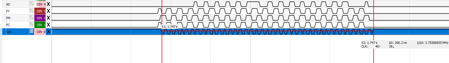
And regarding logic analyser, it can able to analyse at 800 MHZ.