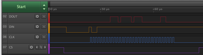
Another thing with the EEPROM (Flash), since it shares its pins with the SD card, it's wise to use SPI cmode 3 rather than cmode 0. This is because selecting SD or EEPROM is done by which pin, of CLK or CE, transitions low first. The standard practice is to setup the clock's smartpin before selecting the chip. In cmode 0, with CPOL=0, this setup lower's the CLK pin, which then selects the wrong chip. Whereas, in cmode 3, with CPOL=1, the CLK pin stays high until clock pulses are sent.
@rogloh said:
Also the trend for price is that PSRAM is cheaper. In low to medium quantities Digikey is selling 64Mbit HyperRAMs for ~$8 (1.8V), and 128Mbit parts for ~$11 but you can pickup the new octal 128Mbit PSRAMs for around $4.60 at Mouser (at 3V). That Digikey linked stuff is kinda moot though for the P2 use because they are 1.8V parts.
I doubt that's a difference in one manufacturer's pricing. You're really comparing two retailers there.
PS: The only difference I see between HyperRAM and OPI PSRAM is the command and address format. They are priced the same, same package, same pinout, and same electrical and timing interface.
HyperBus is suited to a hardware controller, while SPI like commands are suited to bit-bashing.
@evanh said:
Another thing with the EEPROM (Flash), since it shares its pins with the SD card, it's wise to use SPI cmode 3 rather than cmode 0. This is because selecting SD or EEPROM is done by which pin, of CLK or CE, transitions low first. The standard practice is to setup the clock's smartpin before selecting the chip. In cmode 0, with CPOL=0, this setup lower's the CLK pin, which then selects the wrong chip. Whereas, in cmode 3, with CPOL=1, the CLK pin stays high until clock pulses are sent.
Yeah I have been thinking the same, although without extra software controls a COG using the SD can corrupt another doing a FLASH access and vice versa. But it's nice to have the idle condition as both CLK & CE pins high. Also they could change the state of the smartpins/pinconfigs for data remap at any time as well.
I do already have the concept of a software lock for FLASH accesses which is typically used when programming it by a COG so other priority COGs making FLASH requests will return BUSY failure codes or will have their mailbox requests automatically deferred until the FLASH is free if they are round-robin polled. This prevents lockups.
To correctly co-exist with a COG desiring SD access, it may be possible to have the SD driver COG lock the FLASH each time it needs to access the SD by performing a mailbox operation or calling a SPIN2 API. This would be a reasonably fast operation to perform (~microseconds) if the SD COG is given decent priority and could be done before a bunch of SD sectors get read/written and released afterwards. This scheme would allow co-existence of FLASH readers, SD readers/writers and PSRAM readers/writers, with only the SD users and any FLASH writers needing to request the lock. All round-robin COG FLASH readers would get delayed when the SD is actively in use but not be affected otherwise, and not have to manage the pins themselves.
I look at it the other direction - Only a single integrated application, with all resources at its disposal. No OS layers. But SD card can be slotted alongside the EEPROM. Most likely only one of the two is in use. The hardware just has to be sequenced right to play nice.
These Winbond QPI flash chips are getting quite large now. 256MB chips can already be obtained which is the limit of my driver (per bus). You could put two devices in parallel (8 bit) and read them out at the same time from the same address to get up to 133MB/s without overclocking, although writing is more complicated as you'd need to poll both if they complete their writes at different times.
So it might be possible to put two smaller 512Mbit devices on a board (using 12 P2 pins) or a ROM cartridge to reach 128MB and run NeoYume directly from it in QPI mode (maybe using sysclk/3 too if these chips are not overclockable to 168MHz or so from 133MHz). Of course the price to do so is probably high. But it really saves on the load time....
@evanh said:
I look at it the other direction - Only a single integrated application, with all resources at its disposal. No OS layers. But SD card can be slotted alongside the EEPROM. Most likely only one of the two is in use. The hardware just has to be sequenced right to play nice.
With full software control yes it can be easily co-ordinated like that. It's just if you want to run independent COGs that access either device at will then it's a different situation and something needs to manage the access. I don't propose any real OS layers for this though, probably just a simple mailbox call to lock/unlock.
@rogloh said:
These Winbond QPI flash chips are getting quite large now.
Huh, they are 3v3 and SLC too! DRAM should achieve the same density then. Demand for them must be too low.
EDIT: Maybe they are multi-layer Flash ... ah, SLC NAND Flash is denser than NOR Flash, and seemingly by a big margin. I most definitely hadn't picked up on that and don't know why.
@rogloh said:
... It's just if you want to run independent COGs that access either device at will ...
I don't see that happening. About the only time both are needed together is for the special case of a firmware update when normally booting from EEPROM.
@evanh said:
... ah, SLC NAND Flash is denser than NOR Flash, and seemingly by a big margin.
The other detail to mention is read access time: NOR is may half the speed of DRAM whereas NAND is at least a couple hundred times slower. Even worse for MLC.
EDIT: And of course write endurance: DRAM is essentially unlimited, NOR is around 100,000 erases, SLC NAND is 10,000 and it just gets worse for MLC/TLC/QLC.
@rogloh said:
... It's just if you want to run independent COGs that access either device at will ...
I don't see that happening. About the only time both are needed together is for the special case of a firmware update when normally booting from EEPROM.
What about if we had a setup that had no external PSRAM, but wanted to run an emulator out of FLASH and occasionally needed to read/write files on an SD card? Soon it may become possible with my caching stuff to run non-native or even native P2 code from FLASH. I know some people really despise that idea, but whatever...
EDIT: Ideally for this type of thing you would run a different SPI bus to an SD card IMO, but the current P2 boards can/do share the SPI bus and it is convenient for people to still be able to use these setups.
@evanh said:
I saw your posting with WAITXMT so gave it a try but it made almost no difference. I think it was one sysclock tick difference from WAITXFI.
Just realized something here. Unlike DualSPI and QuadSPI/QPI modes, in SPI mode actually there is no need to tri-state the output before reading back DO data when reading a register from the FLASH. This reduces the timing complexity for reads and may allow alignment of input read data with full rate (gapless) clocking as it removes the need to wait for the transmission of the command phase to complete first. The only issue is switching the data pin from registered to unregistered if the neighboring pin remapping is being done at the same time as doing this may affect the output phase. To get around that I could probably try to remove the pin remapping before/after the register transfer. TBD.
Yeah, I separated the SPI routines from the QPI routines in that demo code partly because SPI is full-duplex whereas the others are all half-duplex.
Does register reading require SPI mode? Goes reads datasheet ... So it does! Yet Chip ID can still be read in Dual/Quad modes of the Winbond EEPROM. Go figure.
@rogloh said:
Just realized something here. Unlike DualSPI and QuadSPI/QPI modes, in SPI mode actually there is no need to tri-state the output before reading back DO data when reading a register from the FLASH. This reduces the timing complexity for reads and may allow alignment of input read data with full rate (gapless) clocking as it removes the need to wait for the transmission of the command phase to complete first. The only issue is switching the data pin from registered to unregistered if the neighboring pin remapping is being done at the same time as doing this may affect the output phase. To get around that I could probably try to remove the pin remapping before/after the register transfer. TBD.
Yep, sure enough I was able to get it to work without gapping the clock this way.
Enter command (?=HELP) : S
SPI FLASH SR1 = 00
SPI FLASH SR2 = 00
SPI FLASH SR3 = 60
Flash Device ID & SFDP data:
JEDEC ID          = $1870EF
Here's the code I tried. It works with a range of delay values which can be setup prior in the hub exec code, although it might also need to be adjusted based on sysclk/2, sysclk/3 and sysclk/4 operation.
                            call    #setuprw                'initialize from HUB exec to save space
            if_c            rdfast  bit31, hubdata          'data writes sourced from hub
            if_nc           wrfast  bit31, ptrb             'data reads go to mailbox
                            wxpin   clkdutyflash, #FLASH_CLK_PIN
                            skipf   pattern                 ' R W  (a) register read
                                                            ' E R  (b) register write
                                                            ' A I
                                                            ' D T
                                                            '   E
                                                            '
                            xinit   xcmd, cmdaddr           ' a b           send command byte
                            wypin   wrclks, #FLASH_CLK_PIN  ' a b           start clock output
                            xcont   xaddr1, count           ' ? ?           optionally send address/immediate data
                            xcont   xdata1, hubdata         ' ? ?           optionally send data from hub
        if_z                wrpin   #0, #FLASH_DO_PIN       ' a |           selected registered/unregistered data pins
        if_nz               wrpin   regdatabus,#FLASH_DO_PIN' a |           selected registered/unregistered data pins
                            setq    xfreq1                  ' a |
                            xcont   delay, #0               ' a |           delay
                            setq    xfreq2flash             ' a |
                            xcont   xrecvdata1, ptrb        ' a |           read back bytes to mailbox (up to 64 bits)
                            waitxfi                         ' a b
                            fltl    #FLASH_DATA_PINS        ' a b           tri-state data bus
                            jmp     #wait_to_complete+1     ' a b           save repeating some duplicated instructions
@evanh said:
Does register reading require SPI mode? Goes reads datasheet ... So it does! Yet Chip ID can still be read in Dual/Quad modes of the Winbond EEPROM. Go figure.
Yeah CHIP ID could be read in that mode, but no need, just keep it all SPI based to simplify the register reading code as most things need to be controlled in SPI mode anyway.
Excellent. BTW, those SETQ/XCONT combos would be simpler as just a single WAITX. eg:
                            xinit   xcmd, cmdaddr           ' a b           send command byte
                            wypin   wrclks, #FLASH_CLK_PIN  ' a b           start clock output
                            xcont   xaddr1, count           ' ? ?           optionally send address/immediate data
                            xcont   xdata1, hubdata         ' ? ?           optionally send data from hub
        if_z                wrpin   #0, #FLASH_DO_PIN       ' a |           selected registered/unregistered data pins
        if_nz               wrpin   regdatabus,#FLASH_DO_PIN' a |           selected registered/unregistered data pins
                            waitx   delay                   ' a |
                            xinit   xrecvdata1, ptrb        ' a |           read back bytes to mailbox (up to 64 bits)
                            waitxfi                         ' a b
                            fltl    #FLASH_DATA_PINS        ' a b           tri-state data bus
I've been reading through some of the SFDP stuff and man that gets nasty. By the looks of it this JEDEC agreement seems to try to rationalize/describe the different SPI FLASH device's functionality and has a bunch of different bit fields to identify all sorts of different vendor methods to reset the devices, perform read/writes in 1:1:1, 1:2:2, 1:4:4, 4:4:4, 0:4:4 modes etc, change in/out of QPI mode, enable 32 bit addressing instead of 24 bit, issue erase/program commands etc.
Ideally a general purpose SPI/QPI memory driver could be setup that would allow these different modes to be used/selected and work with a bunch of different vendor's chips. Doesn't make sense so much for the boot flash on the P2 with its restricted pinning and device support, but if there were different vendor's chips on a specific dedicated bus for FLASH with different IO pins then it would be good to have a driver that could do this based on the SFDP information. I started down this path initially but reduced the scope down to just the boot flash to at least get something going faster and have a way to make it fit in with PSRAM (which should be quite useful on the P2-EC32MB).
@evanh said:
Excellent. BTW, those SETQ/XCONT combos would be simpler as just a single WAITX. eg:
                            xinit   xcmd, cmdaddr           ' a b           send command byte
                            wypin   wrclks, #FLASH_CLK_PIN  ' a b           start clock output
                            xcont   xaddr1, count           ' ? ?           optionally send address/immediate data
                            xcont   xdata1, hubdata         ' ? ?           optionally send data from hub
        if_z                wrpin   #0, #FLASH_DO_PIN       ' a |           selected registered/unregistered data pins
        if_nz               wrpin   regdatabus,#FLASH_DO_PIN' a |           selected registered/unregistered data pins
                            waitx   delay                   ' a |
                            xinit   xrecvdata1, ptrb        ' a |           read back bytes to mailbox (up to 64 bits)
                            waitxfi                         ' a b
                            fltl    #FLASH_DATA_PINS        ' a b           tri-state data bus
Yeah perhaps. Also I realized can probably use a temp register and save another COG long with the selection of if_z and if_nz stuff moving to a single instruction using the temp register.
"Serial flash discoverable parameter (SFDP) standard". Oh, man, surely it has to be better than EDID!
My feeling is SD cards work. They are fast at writes and they do the wear levelling for you. That's rather important. I don't have a lot of interest in Flash beyond SD, to honest.
Ah, I just realised one advantage of stopping the clock at the end of CA phase. It allows reliable switching of the clock pin registration under all combinations. I've found I can, without stopping, get away with switching from unregistered to registered but not the reverse. Switching the clock pin from registered to unregistered, without stopping first, messes up every time.
It's not a combination I consider of great value though. So I'm not likely to try supporting that ability. Rather, if the clock is desired to be unregistered for the RX phase, then it can be unregistered for the CA phase too.
Having multiple combinations like this gets rather tricky to manage, and very difficult for an average user to figure it all out. For sysclk/2 or lower I think it's simplest to keep the CA phase registered (both clock and data), and only adjust the data phase for reads, leaving the clock intact throughout. I know we had to jump through hoops for the HyperRAM operation at sysclk/1 though and it became a bit of a nightmare to patch the code dynamically for that in all those combinations. It might be easy if you setup constants in your code but adjusting the code per bank is getting a lot more complicated...although we've both probably learned more since then, so maybe not as bad as HyperRAM. If Rayman's new OPI PSRAM is used with DDR, transferring at sysclk/1 rates, then this might have to be looked at again. Maybe I'll leave that one to you to figure out... I've don't have a board with that RAM anyway.
Actually, now I've got this tester all worked out, I can try that idea out right now on the EC32MB. It'll still be sysclock/2 but I can do all the alignment and reliability testing as if it were sysclock/1 ...
Ah, I bet SPI cmode3 is out of the question. It'll have to be cmode0 ... or not really either, since every edge is supposed to count in full DDR, but CPOL=0 is what's important.
Initial tests are a little suspiciously no change in results, maybe I'm not changing anything ...
Huh, I think it might be right, the tx data is still clocked into the RAM chip on the same rising edge, just that the tx data is only just setup a nanosecond ahead of the rising clock ... and the rx data is exactly as it was - still referenced the same instruction count from clock smartpin startup.
LOL, it's doing this for the SPI routines too.
The requirements are tx data pins to be registered to achieve best skew timing, and clock pin is to be unregistered to provide the clock lag for tx data setup time. And the testing involved just retarding the tx data (CLK_ADV=1) by one sysclock so that it (almost) aligns to the later rising clock edge.
I just gave this DDR-like config a spin using Rayman's 96 MB and 48 MB add-ons. Not a single bank worked at almost any speed. Almost because there were some tiny patches of good frequencies with the 48 MB add-on. Nothing to be happy about.
So, not surprisingly, this approach absolutely requires the correct layout to guarantee the data setup time ahead of every clock edge at sysclock/1.
To be honest, I'm not that confident with the add-on I've drawn up either. It would be nice to put ten variations on a single PCB order. But I'm not sure the contract manufacturers will let me do that without a large fee.
Yeah sysclk/1 DDR is a PITA to get the timing working right. We had some regions with HyperRAM that could do sysclk/1 transfers but from what I recall it wasn't fully overlapping like PSRAM is at sysclk/2 and was still a bit sensitive to temperature. In comparison PSRAM is really quite solid, despite being half speed (although the 16 bit width option sort of makes up for a lot of that).
The EC32MB is perfect, timing wise. It breezes through the sudo-DDR timing test. So that's a known good reference. One thing the EC32MB has is a common clock going to all four parts, so four loads on the clock pin, while only a single load on each of the 16 data pins.
A real advantage that won't easily be replicated with 8-bit parts. EDIT: But I suspect that's not a necessity as long as everything else is done to give the data pins the edge over the clock pin. Ie: The Hyperbus add-on board fell over badly on double loading the data pins but only a single load on the clocks.
You brought up the read-modify-write topic as I was finishing up my demo code - That's something that is new because of the EC32MB wiring isn't it. Because it can only be written 32-bit at a time, right?
Question: Is the RWDS signalling worth it on the 8-bit parts? If that was to be utilised as 2 x 8-bit = 16-bit bus width it would need two RWDS pins. A total of 20 compared to only 18 pins on the EC32MB.
@evanh said:
You brought up the read-modify-write topic as I was finishing up my demo code - That's something that is new because of the EC32MB wiring isn't it. Because it can only be written 32-bit at a time, right?
Yes. If it's wired as a 16 bit bus then with two cycles per write, only a complete 32 bit long should be written at a time. So to avoid data corruption in the memory both upper and lower 16 bits need to be written whenever a write is performed, and this necessitates a read first. You can't start writing half way into the long, you need to start from the beginning after CE is brought low, and there is no data qualifier brought out (unlike the OPI PSRAM).
Question: Is the RWDS signalling worth it on the 8-bit parts? If that was to be utilised as 2 x 8-bit = 16-bit bus width it would need two RWDS pins. A total of 20 compared to only 18 pins on the EC32MB.
RWDS as a write qualifier is worth it to avoid the extra RMW requirements for HyperRAM which is natively accessed as 16 bits internally. It is far less useful as a read strobe on the P2 however, especially if fixed latency is used.
The logic and timing to control a pair of RWDS pin is going to be tricky. I used a smartpin in a particular way to generate the RWDS and the timing was complicated. It's also a bidirectional signal making it even trickier to control.
@evanh said:
I guess that's my next objective: Nut out all the options for managing multiple write qualifiers to eliminate the need for read-modify-write.
Are you planning on a pair of OPI PSRAMs, or a pair of HyperRAMs?


Comments
Another thing with the EEPROM (Flash), since it shares its pins with the SD card, it's wise to use SPI cmode 3 rather than cmode 0. This is because selecting SD or EEPROM is done by which pin, of CLK or CE, transitions low first. The standard practice is to setup the clock's smartpin before selecting the chip. In cmode 0, with CPOL=0, this setup lower's the CLK pin, which then selects the wrong chip. Whereas, in cmode 3, with CPOL=1, the CLK pin stays high until clock pulses are sent.
I doubt that's a difference in one manufacturer's pricing. You're really comparing two retailers there.
PS: The only difference I see between HyperRAM and OPI PSRAM is the command and address format. They are priced the same, same package, same pinout, and same electrical and timing interface.
HyperBus is suited to a hardware controller, while SPI like commands are suited to bit-bashing.
Yeah I have been thinking the same, although without extra software controls a COG using the SD can corrupt another doing a FLASH access and vice versa. But it's nice to have the idle condition as both CLK & CE pins high. Also they could change the state of the smartpins/pinconfigs for data remap at any time as well.
Agree, it's not apples to apples there.
I do already have the concept of a software lock for FLASH accesses which is typically used when programming it by a COG so other priority COGs making FLASH requests will return BUSY failure codes or will have their mailbox requests automatically deferred until the FLASH is free if they are round-robin polled. This prevents lockups.
To correctly co-exist with a COG desiring SD access, it may be possible to have the SD driver COG lock the FLASH each time it needs to access the SD by performing a mailbox operation or calling a SPIN2 API. This would be a reasonably fast operation to perform (~microseconds) if the SD COG is given decent priority and could be done before a bunch of SD sectors get read/written and released afterwards. This scheme would allow co-existence of FLASH readers, SD readers/writers and PSRAM readers/writers, with only the SD users and any FLASH writers needing to request the lock. All round-robin COG FLASH readers would get delayed when the SD is actively in use but not be affected otherwise, and not have to manage the pins themselves.
This would probably be ideal.
I look at it the other direction - Only a single integrated application, with all resources at its disposal. No OS layers. But SD card can be slotted alongside the EEPROM. Most likely only one of the two is in use. The hardware just has to be sequenced right to play nice.
These Winbond QPI flash chips are getting quite large now. 256MB chips can already be obtained which is the limit of my driver (per bus). You could put two devices in parallel (8 bit) and read them out at the same time from the same address to get up to 133MB/s without overclocking, although writing is more complicated as you'd need to poll both if they complete their writes at different times.
So it might be possible to put two smaller 512Mbit devices on a board (using 12 P2 pins) or a ROM cartridge to reach 128MB and run NeoYume directly from it in QPI mode (maybe using sysclk/3 too if these chips are not overclockable to 168MHz or so from 133MHz). Of course the price to do so is probably high. But it really saves on the load time....
With full software control yes it can be easily co-ordinated like that. It's just if you want to run independent COGs that access either device at will then it's a different situation and something needs to manage the access. I don't propose any real OS layers for this though, probably just a simple mailbox call to lock/unlock.
Huh, they are 3v3 and SLC too! DRAM should achieve the same density then. Demand for them must be too low.
EDIT: Maybe they are multi-layer Flash ... ah, SLC NAND Flash is denser than NOR Flash, and seemingly by a big margin. I most definitely hadn't picked up on that and don't know why.
I don't see that happening. About the only time both are needed together is for the special case of a firmware update when normally booting from EEPROM.
The other detail to mention is read access time: NOR is may half the speed of DRAM whereas NAND is at least a couple hundred times slower. Even worse for MLC.
EDIT: And of course write endurance: DRAM is essentially unlimited, NOR is around 100,000 erases, SLC NAND is 10,000 and it just gets worse for MLC/TLC/QLC.
What about if we had a setup that had no external PSRAM, but wanted to run an emulator out of FLASH and occasionally needed to read/write files on an SD card? Soon it may become possible with my caching stuff to run non-native or even native P2 code from FLASH. I know some people really despise that idea, but whatever...
EDIT: Ideally for this type of thing you would run a different SPI bus to an SD card IMO, but the current P2 boards can/do share the SPI bus and it is convenient for people to still be able to use these setups.
Just realized something here. Unlike DualSPI and QuadSPI/QPI modes, in SPI mode actually there is no need to tri-state the output before reading back DO data when reading a register from the FLASH. This reduces the timing complexity for reads and may allow alignment of input read data with full rate (gapless) clocking as it removes the need to wait for the transmission of the command phase to complete first. The only issue is switching the data pin from registered to unregistered if the neighboring pin remapping is being done at the same time as doing this may affect the output phase. To get around that I could probably try to remove the pin remapping before/after the register transfer. TBD.
Yeah, I separated the SPI routines from the QPI routines in that demo code partly because SPI is full-duplex whereas the others are all half-duplex.
Does register reading require SPI mode? Goes reads datasheet ... So it does! Yet Chip ID can still be read in Dual/Quad modes of the Winbond EEPROM. Go figure.
Yep, sure enough I was able to get it to work without gapping the clock this way.
Here's the code I tried. It works with a range of delay values which can be setup prior in the hub exec code, although it might also need to be adjusted based on sysclk/2, sysclk/3 and sysclk/4 operation.
call #setuprw 'initialize from HUB exec to save space if_c rdfast bit31, hubdata 'data writes sourced from hub if_nc wrfast bit31, ptrb 'data reads go to mailbox wxpin clkdutyflash, #FLASH_CLK_PIN skipf pattern ' R W (a) register read ' E R (b) register write ' A I ' D T ' E ' xinit xcmd, cmdaddr ' a b send command byte wypin wrclks, #FLASH_CLK_PIN ' a b start clock output xcont xaddr1, count ' ? ? optionally send address/immediate data xcont xdata1, hubdata ' ? ? optionally send data from hub if_z wrpin #0, #FLASH_DO_PIN ' a | selected registered/unregistered data pins if_nz wrpin regdatabus,#FLASH_DO_PIN' a | selected registered/unregistered data pins setq xfreq1 ' a | xcont delay, #0 ' a | delay setq xfreq2flash ' a | xcont xrecvdata1, ptrb ' a | read back bytes to mailbox (up to 64 bits) waitxfi ' a b fltl #FLASH_DATA_PINS ' a b tri-state data bus jmp #wait_to_complete+1 ' a b save repeating some duplicated instructionsYeah CHIP ID could be read in that mode, but no need, just keep it all SPI based to simplify the register reading code as most things need to be controlled in SPI mode anyway.
Excellent. BTW, those SETQ/XCONT combos would be simpler as just a single WAITX. eg:
xinit xcmd, cmdaddr ' a b send command byte wypin wrclks, #FLASH_CLK_PIN ' a b start clock output xcont xaddr1, count ' ? ? optionally send address/immediate data xcont xdata1, hubdata ' ? ? optionally send data from hub if_z wrpin #0, #FLASH_DO_PIN ' a | selected registered/unregistered data pins if_nz wrpin regdatabus,#FLASH_DO_PIN' a | selected registered/unregistered data pins waitx delay ' a | xinit xrecvdata1, ptrb ' a | read back bytes to mailbox (up to 64 bits) waitxfi ' a b fltl #FLASH_DATA_PINS ' a b tri-state data busI've been reading through some of the SFDP stuff and man that gets nasty. By the looks of it this JEDEC agreement seems to try to rationalize/describe the different SPI FLASH device's functionality and has a bunch of different bit fields to identify all sorts of different vendor methods to reset the devices, perform read/writes in 1:1:1, 1:2:2, 1:4:4, 4:4:4, 0:4:4 modes etc, change in/out of QPI mode, enable 32 bit addressing instead of 24 bit, issue erase/program commands etc.
Ideally a general purpose SPI/QPI memory driver could be setup that would allow these different modes to be used/selected and work with a bunch of different vendor's chips. Doesn't make sense so much for the boot flash on the P2 with its restricted pinning and device support, but if there were different vendor's chips on a specific dedicated bus for FLASH with different IO pins then it would be good to have a driver that could do this based on the SFDP information. I started down this path initially but reduced the scope down to just the boot flash to at least get something going faster and have a way to make it fit in with PSRAM (which should be quite useful on the P2-EC32MB).
See this for SFDP details and you can see how the Winbond data works out from the logs above:
https://www.micron.com/-/media/client/global/documents/products/technical-note/nor-flash/tn2506_sfdp_for_mt25q.pdf
This driver header also gives some details...
https://git.furworks.de/coreboot-mirror/chrome-ec/commit/f8f0618ca4baf7bee03bebefe083c3911a77e52b
Yeah perhaps. Also I realized can probably use a temp register and save another COG long with the selection of if_z and if_nz stuff moving to a single instruction using the temp register.
"Serial flash discoverable parameter (SFDP) standard". Oh, man, surely it has to be better than EDID!
My feeling is SD cards work. They are fast at writes and they do the wear levelling for you. That's rather important. I don't have a lot of interest in Flash beyond SD, to honest.
On that note, be wary of NAND Flash's slow read access. It's measured in microseconds rather than nanoseconds.
EDIT: Found it, it's called tRD. I'm seeing 100 us in the ISSI datasheet, and 50 us in the Winbond datasheet.
Ah, I just realised one advantage of stopping the clock at the end of CA phase. It allows reliable switching of the clock pin registration under all combinations. I've found I can, without stopping, get away with switching from unregistered to registered but not the reverse. Switching the clock pin from registered to unregistered, without stopping first, messes up every time.
It's not a combination I consider of great value though. So I'm not likely to try supporting that ability. Rather, if the clock is desired to be unregistered for the RX phase, then it can be unregistered for the CA phase too.
Having multiple combinations like this gets rather tricky to manage, and very difficult for an average user to figure it all out. For sysclk/2 or lower I think it's simplest to keep the CA phase registered (both clock and data), and only adjust the data phase for reads, leaving the clock intact throughout. I know we had to jump through hoops for the HyperRAM operation at sysclk/1 though and it became a bit of a nightmare to patch the code dynamically for that in all those combinations. It might be easy if you setup constants in your code but adjusting the code per bank is getting a lot more complicated...although we've both probably learned more since then, so maybe not as bad as HyperRAM. If Rayman's new OPI PSRAM is used with DDR, transferring at sysclk/1 rates, then this might have to be looked at again. Maybe I'll leave that one to you to figure out... I've don't have a board with that RAM anyway.
Actually, now I've got this tester all worked out, I can try that idea out right now on the EC32MB. It'll still be sysclock/2 but I can do all the alignment and reliability testing as if it were sysclock/1 ...
Ah, I bet SPI cmode3 is out of the question. It'll have to be cmode0 ... or not really either, since every edge is supposed to count in full DDR, but CPOL=0 is what's important.
Initial tests are a little suspiciously no change in results, maybe I'm not changing anything ...
Huh, I think it might be right, the tx data is still clocked into the RAM chip on the same rising edge, just that the tx data is only just setup a nanosecond ahead of the rising clock ... and the rx data is exactly as it was - still referenced the same instruction count from clock smartpin startup.
LOL, it's doing this for the SPI routines too.
The requirements are tx data pins to be registered to achieve best skew timing, and clock pin is to be unregistered to provide the clock lag for tx data setup time. And the testing involved just retarding the tx data (CLK_ADV=1) by one sysclock so that it (almost) aligns to the later rising clock edge.
usb-Parallax_Inc_PropPlug_P7ehkogg-if00-port0 DATA_PIN = 40 addpins 15 CLK_PIN = 56 addpins 0 CE_PIN = 57 addpins 0 SPI cmode3 TX_REGD = 1 CLK_REGD = 0 CLK_ADV = 1 SPI clock ratio = 2 (sysclock/2) bus[15:12] Chip ID: 0d 5d 52 d5 b5 58 e2 7c bus[11:8] Chip ID: 0d 5d 52 d5 b5 58 b2 7c bus[7:4] Chip ID: 0d 5d 52 d5 b5 58 a8 c8 bus[3:0] Chip ID: 0d 5d 52 d5 b5 57 25 8b Test data length: 100 x 4096 = 409600 bytes Frequency dependent lag compensation Sysclock u0 r0 u1 r1 u2 r2 u3 r3 u4 r4 u5 r5 60 MHz 100% 100% 100% 100% 0% 0% 0% 0% 0% 0% 0% 0% 62 MHz 100% 100% 100% 100% 0% 0% 0% 0% 0% 0% 0% 0% 64 MHz 100% 100% 100% 100% 0% 0% 0% 0% 0% 0% 0% 0% 66 MHz 100% 100% 100% 100% 0% 0% 0% 0% 0% 0% 0% 0% 68 MHz 100% 100% 100% 100% 0% 0% 0% 0% 0% 0% 0% 0% 70 MHz 100% 100% 100% 100% 0% 0% 0% 0% 0% 0% 0% 0% 72 MHz 100% 100% 100% 100% 0% 0% 0% 0% 0% 0% 0% 0% 74 MHz 100% 100% 100% 100% 0% 0% 0% 0% 0% 0% 0% 0% 76 MHz 100% 100% 100% 100% 0% 0% 0% 0% 0% 0% 0% 0% 78 MHz 100% 100% 100% 100% 0% 0% 0% 0% 0% 0% 0% 0% 80 MHz 100% 100% 100% 100% 0% 0% 0% 0% 0% 0% 0% 0% 82 MHz 100% 100% 100% 100% 0% 0% 0% 0% 0% 0% 0% 0% 84 MHz 100% 100% 100% 100% 0% 0% 0% 0% 0% 0% 0% 0% 86 MHz 100% 100% 100% 100% 0% 0% 0% 0% 0% 0% 0% 0% 88 MHz 100% 100% 100% 100% 0% 0% 0% 0% 0% 0% 0% 0% 90 MHz 100% 100% 100% 100% 0% 0% 0% 0% 0% 0% 0% 0% 92 MHz 100% 100% 100% 100% 0% 0% 0% 0% 0% 0% 0% 0% 94 MHz 100% 100% 100% 100% 0% 0% 0% 0% 0% 0% 0% 0% 96 MHz 99% 100% 100% 100% 0% 0% 0% 0% 0% 0% 0% 0% 98 MHz 76% 100% 100% 100% 0% 0% 0% 0% 0% 0% 0% 0% 100 MHz 17% 100% 100% 100% 0% 0% 0% 0% 0% 0% 0% 0% 102 MHz 4% 100% 100% 100% 0% 0% 0% 0% 0% 0% 0% 0% 104 MHz 0% 100% 100% 100% 0% 0% 0% 0% 0% 0% 0% 0% 106 MHz 0% 100% 100% 100% 0% 0% 0% 0% 0% 0% 0% 0% 108 MHz 0% 100% 100% 100% 1% 0% 0% 0% 0% 0% 0% 0% 110 MHz 0% 100% 100% 100% 84% 0% 0% 0% 0% 0% 0% 0% 112 MHz 0% 100% 100% 100% 100% 0% 0% 0% 0% 0% 0% 0% 114 MHz 0% 100% 100% 100% 100% 0% 0% 0% 0% 0% 0% 0% 116 MHz 0% 100% 100% 100% 100% 0% 0% 0% 0% 0% 0% 0% 118 MHz 0% 100% 100% 100% 100% 0% 0% 0% 0% 0% 0% 0% 120 MHz 0% 99% 100% 100% 100% 0% 0% 0% 0% 0% 0% 0% 122 MHz 0% 99% 100% 100% 100% 0% 0% 0% 0% 0% 0% 0% 124 MHz 0% 98% 100% 100% 100% 0% 0% 0% 0% 0% 0% 0% 126 MHz 0% 80% 100% 100% 100% 0% 0% 0% 0% 0% 0% 0% 128 MHz 0% 39% 100% 100% 100% 0% 0% 0% 0% 0% 0% 0% 130 MHz 0% 15% 100% 100% 100% 0% 0% 0% 0% 0% 0% 0% 132 MHz 0% 5% 100% 100% 100% 0% 0% 0% 0% 0% 0% 0% 134 MHz 0% 1% 100% 100% 100% 0% 0% 0% 0% 0% 0% 0% 136 MHz 0% 0% 100% 100% 100% 0% 0% 0% 0% 0% 0% 0% 138 MHz 0% 0% 100% 100% 100% 0% 0% 0% 0% 0% 0% 0% 140 MHz 0% 0% 100% 100% 100% 0% 0% 0% 0% 0% 0% 0% 142 MHz 0% 0% 100% 100% 100% 0% 0% 0% 0% 0% 0% 0% 144 MHz 0% 0% 100% 100% 100% 7% 0% 0% 0% 0% 0% 0% 146 MHz 0% 0% 100% 100% 100% 68% 0% 0% 0% 0% 0% 0% 148 MHz 0% 0% 100% 100% 100% 99% 0% 0% 0% 0% 0% 0% 150 MHz 0% 0% 100% 100% 100% 100% 0% 0% 0% 0% 0% 0% 152 MHz 0% 0% 100% 100% 100% 100% 0% 0% 0% 0% 0% 0% 154 MHz 0% 0% 100% 100% 100% 100% 0% 0% 0% 0% 0% 0% 156 MHz 0% 0% 100% 100% 100% 100% 0% 0% 0% 0% 0% 0% 158 MHz 0% 0% 100% 100% 100% 100% 0% 0% 0% 0% 0% 0% 160 MHz 0% 0% 100% 100% 100% 100% 0% 0% 0% 0% 0% 0% 162 MHz 0% 0% 100% 100% 100% 100% 0% 0% 0% 0% 0% 0% 164 MHz 0% 0% 100% 100% 100% 100% 0% 0% 0% 0% 0% 0% 166 MHz 0% 0% 100% 100% 100% 100% 0% 0% 0% 0% 0% 0% 168 MHz 0% 0% 100% 100% 100% 100% 0% 0% 0% 0% 0% 0% 170 MHz 0% 0% 100% 100% 100% 100% 0% 0% 0% 0% 0% 0% 172 MHz 0% 0% 100% 100% 100% 100% 0% 0% 0% 0% 0% 0% 174 MHz 0% 0% 100% 100% 100% 100% 0% 0% 0% 0% 0% 0% 176 MHz 0% 0% 100% 100% 100% 100% 0% 0% 0% 0% 0% 0% 178 MHz 0% 0% 100% 100% 100% 100% 0% 0% 0% 0% 0% 0% 180 MHz 0% 0% 100% 100% 100% 100% 0% 0% 0% 0% 0% 0% 182 MHz 0% 0% 100% 100% 100% 100% 0% 0% 0% 0% 0% 0% 184 MHz 0% 0% 100% 100% 100% 100% 0% 0% 0% 0% 0% 0% 186 MHz 0% 0% 100% 100% 100% 100% 0% 0% 0% 0% 0% 0% 188 MHz 0% 0% 99% 100% 100% 100% 0% 0% 0% 0% 0% 0% 190 MHz 0% 0% 99% 100% 100% 100% 0% 0% 0% 0% 0% 0% 192 MHz 0% 0% 98% 100% 100% 100% 0% 0% 0% 0% 0% 0% 194 MHz 0% 0% 85% 100% 100% 100% 0% 0% 0% 0% 0% 0% 196 MHz 0% 0% 54% 100% 100% 100% 0% 0% 0% 0% 0% 0% 198 MHz 0% 0% 21% 100% 100% 100% 0% 0% 0% 0% 0% 0% 200 MHz 0% 0% 11% 100% 100% 100% 0% 0% 0% 0% 0% 0% 202 MHz 0% 0% 5% 100% 100% 100% 0% 0% 0% 0% 0% 0% 204 MHz 0% 0% 2% 100% 100% 100% 0% 0% 0% 0% 0% 0% 206 MHz 0% 0% 0% 100% 100% 100% 0% 0% 0% 0% 0% 0% 208 MHz 0% 0% 0% 100% 100% 100% 0% 0% 0% 0% 0% 0% 210 MHz 0% 0% 0% 100% 100% 100% 0% 0% 0% 0% 0% 0% 212 MHz 0% 0% 0% 100% 100% 100% 0% 0% 0% 0% 0% 0% 214 MHz 0% 0% 0% 100% 100% 100% 0% 0% 0% 0% 0% 0% 216 MHz 0% 0% 0% 100% 100% 100% 4% 0% 0% 0% 0% 0% 218 MHz 0% 0% 0% 100% 100% 100% 61% 0% 0% 0% 0% 0% 220 MHz 0% 0% 0% 100% 100% 100% 97% 0% 0% 0% 0% 0% 222 MHz 0% 0% 0% 100% 100% 100% 100% 0% 0% 0% 0% 0% 224 MHz 0% 0% 0% 100% 100% 100% 100% 0% 0% 0% 0% 0% 226 MHz 0% 0% 0% 100% 100% 100% 100% 0% 0% 0% 0% 0% 228 MHz 0% 0% 0% 100% 100% 100% 100% 0% 0% 0% 0% 0% 230 MHz 0% 0% 0% 100% 100% 100% 100% 0% 0% 0% 0% 0% 232 MHz 0% 0% 0% 100% 100% 100% 100% 0% 0% 0% 0% 0% 234 MHz 0% 0% 0% 100% 100% 100% 100% 0% 0% 0% 0% 0% 236 MHz 0% 0% 0% 100% 100% 100% 100% 0% 0% 0% 0% 0% 238 MHz 0% 0% 0% 100% 100% 100% 100% 0% 0% 0% 0% 0% 240 MHz 0% 0% 0% 99% 100% 100% 100% 0% 0% 0% 0% 0% 242 MHz 0% 0% 0% 99% 100% 100% 100% 0% 0% 0% 0% 0% 244 MHz 0% 0% 0% 99% 100% 100% 100% 0% 0% 0% 0% 0% 246 MHz 0% 0% 0% 99% 100% 100% 100% 0% 0% 0% 0% 0% 248 MHz 0% 0% 0% 96% 100% 100% 100% 0% 0% 0% 0% 0% 250 MHz 0% 0% 0% 84% 100% 100% 100% 0% 0% 0% 0% 0% 252 MHz 0% 0% 0% 65% 100% 100% 100% 0% 0% 0% 0% 0% 254 MHz 0% 0% 0% 43% 100% 100% 100% 0% 0% 0% 0% 0% 256 MHz 0% 0% 0% 24% 100% 100% 100% 0% 0% 0% 0% 0% 258 MHz 0% 0% 0% 17% 100% 100% 100% 0% 0% 0% 0% 0% 260 MHz 0% 0% 0% 11% 100% 100% 100% 0% 0% 0% 0% 0% 262 MHz 0% 0% 0% 6% 100% 100% 100% 0% 0% 0% 0% 0% 264 MHz 0% 0% 0% 3% 100% 100% 100% 0% 0% 0% 0% 0% 266 MHz 0% 0% 0% 2% 100% 100% 100% 0% 0% 0% 0% 0% 268 MHz 0% 0% 0% 1% 100% 100% 100% 0% 0% 0% 0% 0% 270 MHz 0% 0% 0% 0% 100% 100% 100% 0% 0% 0% 0% 0% 272 MHz 0% 0% 0% 0% 100% 100% 100% 0% 0% 0% 0% 0% 274 MHz 0% 0% 0% 0% 100% 100% 100% 0% 0% 0% 0% 0% 276 MHz 0% 0% 0% 0% 100% 100% 100% 0% 0% 0% 0% 0% 278 MHz 0% 0% 0% 0% 100% 100% 100% 0% 0% 0% 0% 0% 280 MHz 0% 0% 0% 0% 100% 100% 100% 0% 0% 0% 0% 0% 282 MHz 0% 0% 0% 0% 99% 100% 100% 0% 0% 0% 0% 0% 284 MHz 0% 0% 0% 0% 99% 100% 100% 0% 0% 0% 0% 0% 286 MHz 0% 0% 0% 0% 98% 100% 100% 2% 0% 0% 0% 0% 288 MHz 0% 0% 0% 0% 92% 100% 100% 19% 0% 0% 0% 0% 290 MHz 0% 0% 0% 0% 74% 100% 100% 56% 0% 0% 0% 0% 292 MHz 0% 0% 0% 0% 52% 100% 100% 90% 0% 0% 0% 0% 294 MHz 0% 0% 0% 0% 26% 100% 100% 99% 0% 0% 0% 0% 296 MHz 0% 0% 0% 0% 16% 100% 100% 100% 0% 0% 0% 0% 298 MHz 0% 0% 0% 0% 9% 100% 100% 100% 0% 0% 0% 0% 300 MHz 0% 0% 0% 0% 6% 100% 100% 100% 0% 0% 0% 0% 302 MHz 0% 0% 0% 0% 4% 100% 100% 100% 0% 0% 0% 0% 304 MHz 0% 0% 0% 0% 2% 100% 100% 100% 0% 0% 0% 0% 306 MHz 0% 0% 0% 0% 1% 100% 100% 100% 0% 0% 0% 0% 308 MHz 0% 0% 0% 0% 0% 100% 100% 100% 0% 0% 0% 0% 310 MHz 0% 0% 0% 0% 0% 100% 100% 100% 0% 0% 0% 0% 312 MHz 0% 0% 0% 0% 0% 100% 100% 100% 0% 0% 0% 0% 314 MHz 0% 0% 0% 0% 0% 100% 100% 100% 0% 0% 0% 0% 316 MHz 0% 0% 0% 0% 0% 100% 100% 100% 0% 0% 0% 0% 318 MHz 0% 0% 0% 0% 0% 100% 100% 100% 0% 0% 0% 0% 320 MHz 0% 0% 0% 0% 0% 100% 100% 100% 0% 0% 0% 0% 322 MHz 0% 0% 0% 0% 0% 100% 100% 100% 13% 0% 0% 0% 324 MHz 0% 0% 0% 0% 0% 100% 100% 100% 57% 0% 0% 0% 326 MHz 0% 0% 0% 0% 0% 100% 100% 100% 91% 0% 0% 0% 328 MHz 0% 0% 0% 0% 0% 100% 100% 100% 99% 0% 0% 0% 330 MHz 0% 0% 0% 0% 0% 100% 100% 100% 100% 0% 0% 0% 332 MHz 0% 0% 0% 0% 0% 100% 100% 100% 100% 0% 0% 0% 334 MHz 0% 0% 0% 0% 0% 100% 100% 100% 100% 0% 0% 0% 336 MHz 0% 0% 0% 0% 0% 100% 100% 100% 100% 0% 0% 0% 338 MHz 0% 0% 0% 0% 0% 100% 100% 100% 100% 0% 0% 0% 340 MHz 0% 0% 0% 0% 0% 100% 100% 100% 100% 0% 0% 0% 342 MHz 0% 0% 0% 0% 0% 100% 100% 100% 100% 0% 0% 0% 344 MHz 0% 0% 0% 0% 0% 100% 100% 100% 100% 0% 0% 0% 346 MHz 0% 0% 0% 0% 0% 100% 100% 100% 100% 0% 0% 0% 348 MHz 0% 0% 0% 0% 0% 100% 100% 100% 100% 0% 0% 0% 350 MHz 0% 0% 0% 0% 0% 99% 100% 100% 100% 0% 0% 0% 352 MHz 0% 0% 0% 0% 0% 91% 100% 100% 100% 0% 0% 0% 354 MHz 0% 0% 0% 0% 0% 24% 100% 100% 100% 0% 0% 0% 356 MHz 0% 0% 0% 0% 0% 0% 100% 99% 100% 0% 0% 0% 358 MHz 0% 0% 0% 0% 0% 0% 100% 99% 100% 0% 0% 0% 360 MHz 0% 0% 0% 0% 0% 0% 100% 99% 100% 0% 0% 0%I just gave this DDR-like config a spin using Rayman's 96 MB and 48 MB add-ons. Not a single bank worked at almost any speed. Almost because there were some tiny patches of good frequencies with the 48 MB add-on. Nothing to be happy about.
So, not surprisingly, this approach absolutely requires the correct layout to guarantee the data setup time ahead of every clock edge at sysclock/1.
To be honest, I'm not that confident with the add-on I've drawn up either. It would be nice to put ten variations on a single PCB order. But I'm not sure the contract manufacturers will let me do that without a large fee.
Yeah sysclk/1 DDR is a PITA to get the timing working right. We had some regions with HyperRAM that could do sysclk/1 transfers but from what I recall it wasn't fully overlapping like PSRAM is at sysclk/2 and was still a bit sensitive to temperature. In comparison PSRAM is really quite solid, despite being half speed (although the 16 bit width option sort of makes up for a lot of that).
The EC32MB is perfect, timing wise. It breezes through the sudo-DDR timing test. So that's a known good reference. One thing the EC32MB has is a common clock going to all four parts, so four loads on the clock pin, while only a single load on each of the 16 data pins.
A real advantage that won't easily be replicated with 8-bit parts. EDIT: But I suspect that's not a necessity as long as everything else is done to give the data pins the edge over the clock pin. Ie: The Hyperbus add-on board fell over badly on double loading the data pins but only a single load on the clocks.
You brought up the read-modify-write topic as I was finishing up my demo code - That's something that is new because of the EC32MB wiring isn't it. Because it can only be written 32-bit at a time, right?
Question: Is the RWDS signalling worth it on the 8-bit parts? If that was to be utilised as 2 x 8-bit = 16-bit bus width it would need two RWDS pins. A total of 20 compared to only 18 pins on the EC32MB.
Yes. If it's wired as a 16 bit bus then with two cycles per write, only a complete 32 bit long should be written at a time. So to avoid data corruption in the memory both upper and lower 16 bits need to be written whenever a write is performed, and this necessitates a read first. You can't start writing half way into the long, you need to start from the beginning after CE is brought low, and there is no data qualifier brought out (unlike the OPI PSRAM).
RWDS as a write qualifier is worth it to avoid the extra RMW requirements for HyperRAM which is natively accessed as 16 bits internally. It is far less useful as a read strobe on the P2 however, especially if fixed latency is used.
The logic and timing to control a pair of RWDS pin is going to be tricky. I used a smartpin in a particular way to generate the RWDS and the timing was complicated. It's also a bidirectional signal making it even trickier to control.
I guess that's my next objective: Nut out all the options for managing multiple write qualifiers to eliminate the need for read-modify-write.
Are you planning on a pair of OPI PSRAMs, or a pair of HyperRAMs?