Maybe just tie it to to the P2 reset pin? If the P2 reset pin is like the P1 reset pin, that'd reset on power-up, brownout and external reset. Software reset would have to reset the eMMC in software though (is that even possible?)
which is sampling the rx pin containing the old data byte. New data byte appears after the loop exits. Which in turn is picked up by your posted BlockByteLoop3 loop. And it continues picking up the old/prior bytes - same as my suggestion above - but it clocks one too many as a result.
Was just thinking about this again... Wondering if can share 8-bit bus with PSRAM...
Found some example code googling that says this:
#include "SdMmcPciHcDxe.h"
/**
Send command GO_IDLE_STATE (CMD0 with argument of 0x00000000) to the device to
make it go to Idle State.
Refer to EMMC Electrical Standard Spec 5.1 Section 6.4 for details.
Not sure I can get that electrical spec, but found a datasheet saying bus is in open drain mode in idle state.
So, thinking it should work...
Assuming similar interface protocol to SD cards, deselect (CMD7 with argument of 0x00000000) should be just as good. Any busy signalling on the data pins gets disabled until the card is selected (CMD7 with argument of RCA) again. CMD7 is a lot less hassle than having to re-init the card after each CMD0.
This kind is interesting too. Guessing works in 4-bit mode.
But @rogloh and @evanh have actual SD code coming soon, right?
So, don't really see the point of this...
@evanh said:
Assuming similar interface protocol to SD cards, deselect (CMD7 with argument of 0x00000000) should be just as good. Any busy signalling on the data pins gets disabled until the card is selected (CMD7 with argument of RCA) again. CMD7 is a lot less hassle than having to re-init the card after each CMD0.
But can you do that at any time (i.e. during transfer / wait)? Sharing eMMC/PSRAM bus would be pretty moot if the eMMC side could just hog it for 100s of µs
PS: I've worked out that command acknowledgements always return on the CMD pin and that data acknowledgements always return on the DAT0 pin. You never get the CMD pin suddenly trying to get your attention out of the blue.
@evanh said:
Assuming similar interface protocol to SD cards, deselect (CMD7 with argument of 0x00000000) should be just as good. Any busy signalling on the data pins gets disabled until the card is selected (CMD7 with argument of RCA) again. CMD7 is a lot less hassle than having to re-init the card after each CMD0.
But can you do that at any time (i.e. during transfer / wait)? Sharing eMMC/PSRAM bus would be pretty moot if the eMMC side could just hog it for 100s of µs
Yep, assuming the card is still busy, the busy indication will resume upon reselection. That's the Disconnect State when it's busy and deselected.
I haven't tried this but it looks like CMD7 acts like CMD12 in that it can cancel a data block transfer in mid flight too. No need to first stop a block transfer to deselect a card.
@evanh You got me wondering how close eMMC protocol is to SD protocol... Maybe very similar? Perhaps the only difference is when doing encrypted music and such?
The whole "encrypted ROM card pre-loaded with music" idea was dead-on-arrival anyways, in practice it doesn't exist and I think more recent versions of the spec just axe everything related to that
There's a lot more added to the SD interface and protocol when it gets to wrangling 1.8 Volt with UHS-I and even more for the differential pairs of UHS-II. I think UHS-I added a bunch of buffering extensions and UHS-II removed them again in favour of something else. I presume EMMC doesn't do any of that. Does it have 1.8 Volt switching?
Impressive. Intended for soldered parts obviously. And possibly not switchable, ie: You buy them at the voltage desired. Which will remove all the negotiations and extended command set that SD Cards have.
I note they talk about the 10,000 or 100,000 endurance of Flash, which suggests you also have to do your own wear levelling in the Prop.
Okay, good. And yes, I also consider built in wear levelling very desirable to have. I must have wandered into anther section of the website for simple Flash parts I guess.
There is much that is the same between SD and MMC. And certainly the basic operation is the same.
Modern SD Cards are very good at sustained fast writing. That's another area where basic Flash parts are troublesome. eMMC's close relationship with SD Cards suggests that newer eMMC parts are also good with sustained fast writes.


Comments
[ Moved from emulation topic - https://forums.parallax.com/discussion/comment/1539903/#Comment_1539903 ]
Maybe optimistic there Rayman. Inner loop is sysclock/14:
BlockByteLoop2
                rep     @.end_read,n1
                drvl    pinClk    '2
                nop               '4
                waitx   #2        '8
                drvh    pinClk    '10
                nop               '12
                wfbyte  inb       '14
.end_read
28 MBytes/s, without overheads, would need sysclock of 411 MHz.
BTW: It wouldn't take much to tighten that loop to sysclock/8. Something like:
BlockByteLoop2 drvl pinClk '2 nop '4 drvh pinClk '6 rep @.end_read,#511 drvl pinClk '10 nop '12 drvh pinClk '14 wfbyte inb '16 .end_read waitx #4 wfbyte inbHmm... Been a while, not sure how I messed that up...
Maybe I never posted the fast version...
Just looked and the inner assembly loop is like this:
BlockByteLoop3 rep @.end_read,n1 drvl pinClk drvh pinClk waitx #2 wfbyte inb .end_readAh, that's writing the flash, not reading. Err, no. But that won't work as is. Not enough lag compensation. Or it might just, at slowest sysclocks.
Oh, I see what's going on, you're clocking 513 bytes, which likely doesn't hurt. It starts with this:
WaitStartBit3
                drvl    pinClk
                drvh    pinClk
                nop
                testp   pinBase wc
        if_nc   jmp     #DoReadBlock3
                jmp     #WaitStartBit3
which is sampling the rx pin containing the old data byte. New data byte appears after the loop exits. Which in turn is picked up by your posted BlockByteLoop3 loop. And it continues picking up the old/prior bytes - same as my suggestion above - but it clocks one too many as a result.
A comment in the code says:
' 04JUN20: Multi-block read speed up to 28 MB/s with 300 MHz clock
Yep, sysclock/10 is close to best. You should be able to do this:
BlockByteLoop3 rep @.end_read,#511 drvl pinClk ' 8, low going clocks out from flash nop '2 10 drvh pinClk '4 12 wfbyte inb '6 14 .end_read waitx #4 wfbyte inbTo do any better than sysclock/8 requires frequency calibration. Like what gets done with the PSRAMs.
Was just thinking about this again... Wondering if can share 8-bit bus with PSRAM...
Found some example code googling that says this:
Not sure I can get that electrical spec, but found a datasheet saying bus is in open drain mode in idle state.
So, thinking it should work...
Assuming similar interface protocol to SD cards, deselect (CMD7 with argument of 0x00000000) should be just as good. Any busy signalling on the data pins gets disabled until the card is selected (CMD7 with argument of RCA) again. CMD7 is a lot less hassle than having to re-init the card after each CMD0.
Kind used before is still around:
https://www.friendlyelec.com/index.php?route=product/product&product_id=249
But, see some larger, cheaper ones on Amazon.
Kind of strange connector though. Still, might have to see what pinout looks like...
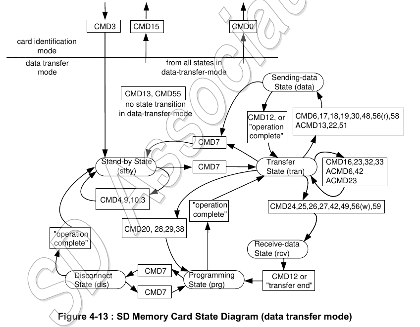
This datasheet seems to suggest that CMD7 (for standby state) should work:
Hopefully this is standard, as you suggest...
This kind is interesting too. Guessing works in 4-bit mode.
But @rogloh and @evanh have actual SD code coming soon, right?
So, don't really see the point of this...
That table is wrong. Stand-by State is part of Data Transfer Mode. But, yes, Stand-by/Disconnect State is what you want.
But can you do that at any time (i.e. during transfer / wait)? Sharing eMMC/PSRAM bus would be pretty moot if the eMMC side could just hog it for 100s of µs
PS: I've worked out that command acknowledgements always return on the CMD pin and that data acknowledgements always return on the DAT0 pin. You never get the CMD pin suddenly trying to get your attention out of the blue.
Yep, assuming the card is still busy, the busy indication will resume upon reselection. That's the Disconnect State when it's busy and deselected.
I haven't tried this but it looks like CMD7 acts like CMD12 in that it can cancel a data block transfer in mid flight too. No need to first stop a block transfer to deselect a card.
@evanh You got me wondering how close eMMC protocol is to SD protocol... Maybe very similar? Perhaps the only difference is when doing encrypted music and such?
The whole "encrypted ROM card pre-loaded with music" idea was dead-on-arrival anyways, in practice it doesn't exist and I think more recent versions of the spec just axe everything related to that
There's a lot more added to the SD interface and protocol when it gets to wrangling 1.8 Volt with UHS-I and even more for the differential pairs of UHS-II. I think UHS-I added a bunch of buffering extensions and UHS-II removed them again in favour of something else. I presume EMMC doesn't do any of that. Does it have 1.8 Volt switching?
Yes, and 1.2 V with HS400 and HS200 modes:
https://bpmmicro.com/hs400-programming-improves-emmc-performance/
Seem to recall using the DDR mode, good for 3 V (and apparently 3.3V).
Impressive. Intended for soldered parts obviously. And possibly not switchable, ie: You buy them at the voltage desired. Which will remove all the negotiations and extended command set that SD Cards have.
I note they talk about the 10,000 or 100,000 endurance of Flash, which suggests you also have to do your own wear levelling in the Prop.
Found this overview of mode changes - https://community.nxp.com/pwmxy87654/attachments/pwmxy87654/imx-solutions@tkb/267/1/eMMC5.0_vs_eMMC5.1_note.pdf
It's similar to SD but different. Doesn't have the voltage switching but does have the speed and strength selections in similar way.
Also, HS400 pinout is notably different to HS200. It's not like UHS-I vs UHS-II though. UHS-II has an extra bus altogether.
wear leveling is a concern. I think SD does this automatically, right? You think eMMC does not?
This suggests it does:
https://www.kingston.com/en/blog/embedded-and-industrial/emmc-lifecycle
Okay, good. And yes, I also consider built in wear levelling very desirable to have. I must have wandered into anther section of the website for simple Flash parts I guess.
There is much that is the same between SD and MMC. And certainly the basic operation is the same.
Modern SD Cards are very good at sustained fast writing. That's another area where basic Flash parts are troublesome. eMMC's close relationship with SD Cards suggests that newer eMMC parts are also good with sustained fast writes.
Just noticed industrial grade eMMC. Think these might be new, didn't notice before...