@Simonius said:
3.7.4.1 REF_CLK In Mode
In REF_CLK In Mode, the 50MHz REF_CLK is driven on the XTAL1/CLKIN pin. A 50MHz source for REF_CLK must
be available external to the device when using this mode. The clock is driven to both the MAC and PHY as shown in
Figure 3-7.
Ok, that solves the riddle of how this was supposed to work on the Waveshare eval board. But I don't use that mode. Instead, I've change it that way:
removed R9 (RXER pullup) and connected RXER to pin header #13
removed R12 and 50MHz oscillator
removed R6 (to LED1), leave REGOFF open/floating
removed R8 (to LED2), connected a pulldown to INTSEL
connected a 25MHz crystal between pin #4 and #5 (XTAL1/XTAL2)
That results in the following configuration:
MODE[2:0] = 111 (same as default)
INTSEL=0, REF_CLK out mode (different from original eval board)
PHYAD0=0 (default)
REGOFF=0 (default), 1.2V regulator enabled
The reason I've done that is because, first, it's the same configuration as on the Amiga board of my friend that has proven to work. Second, I want to get rid of the 50MHz oscillator. I have plenty of 25MHz crystals in stock and want to use a single source to clock both the PHY and the P2. I verified that this works as expected with the scope and by reading back the status registers. So this is not the problem. The LAN8720 outputs a stable 50MHz at REF_CLK and reports a working link.
3.1.2.7: Receive Data Valid Signal
Reception of either the End of Stream Delimiter (ESD) consisting of the /T/R/ symbols, or at least two /I/ symbols causes the transceiver to de-assert the carrier sense and receive data valid signals.
I understand this as CRS_DV should go low during idle phases. However, what I see on the scope is that it stays low during startup and auto-negotioation but is high almost all of the time afterwards. There are only very narrow low pulses taking two or four 50MHz clock periods. Is this normal or is there something wrong?
You'll be running the RMII link asynchronously now. That means needing over-sampling of the rx pins. Streamer use will need more post-processing to cull the excess samples.
The data sheet says that all signals are synchronous to the reference clock except for the rising edge of CRS which might be asynchronous (or synchronous to the remote transmitter clock). But this is not the problem. I'm not using the streamer or sample anything at the moment. I'm just looking at the scope. CRS_DV seems to be perfectly in sync with the rising clock edge of REF_CLK (PHY output to P2).
What's also strange: the auto-negotiation advertisement register and the link partner ability register both show all flags (10&100M full&half duplex). However, the Special status register reads $40 before and $1058 after auto-negotiation. This means it switches to half duplex although both partners support full duplex.
@evanh said:
You'll be running the RMII link asynchronously now.
I still don't understand that fully. The Waveshare board as configured originally has no clock output at all. nINT/REFCLK is configured as interrupt pin and there is no other clock pin to the MAC interface connector. The 50MHz clock, as I know now, is correctly configured for REF_CLK input mode but is only connected locally to XTAL1. So THAT is running asynchronously. If I used the board in that configuration I would have to guess the clock by a magic glass ball or an antenna.
No matter if I use REF_CLK input or output mode, the timing synchronous to the clock is always well defined: see figure 5-4 RMII timing (REF_CLK out mode) and figure 5-5 RMII timing (REF_CLK in mode).
My suggestion would be doable with an existing Prop2 board like the Edge or Eval.
Just setup a smartpin to drive the RXCLK of the LAN board. And obviously change the resistor jumpers to route that to the XI (pin 5) of the LAN8720 chip.
Ok, I think now I understand.
Originally, R12 and R14 were soldered in and R11 left open. In that way the external RXCLK at the pin header and OSCIN to the LAN8720 are both fed with the 50MHz oscillator signal. Pin #14 is configured as nINT but not used at all which makes sense.
I can change my setup to use the second waveshare board with the original configuration. But it shouldn't make much difference. The setup and hold times in figure 5-4 vs. 5-5 are slightly different but all positive and synchronous.
I understand this as CRS_DV should go low during idle phases. However, what I see on the scope is that it stays low during startup and auto-negotioation but is high almost all of the time afterwards. There are only very narrow low pulses taking two or four 50MHz clock periods. Is this normal or is there something wrong?
This is strange. DV / data valid is only high when a packet is received. you would at least see the preamble on the rx0/rx1 pins.
are you sure that tx_en is low? if you send on a half duplex line, CRS might also go up while the line is occupied by the transmitter. (i'm not sure if that really is so)
i would start afresh with the other module. you have done a lot of modding to the pcb which may have caused it to malfunction
@Simonius said:
are you sure that tx_en is low? if you send on a half duplex line, CRS might also go up while the line is occupied by the transmitter. (i'm not sure if that really is so)
That would be a possible explanation. I've checked that TX_EN is really low but that could also be masked by the 1Meg pulldown of the internal resistance of the scope probe. Yes, CRS is active both during transmit and receive when half duplex mode is selected.
basic control register is $3100 (100Mbps, auto-negotiation enabled, full duplex)
basic status register reads $782D (all modes except -T2 enabled, auto-negotiation completed, link up)
auto-negotiation advertisment register is $1E1 (all modes enabled, including 100M full duplex)
auto-negotiation partner ability is $CDE1 (all modes enabled, including 100M full duplex)
but special control register reads $1058 which indicates half duplex
This makes no sense as full duplex should have priority if both partners support it.
To be sure that there is no problem with the config straps (pullup/pulldowns) I've also checked the special mode register which contains $60E0. This is the default MODE[2..0] = %111 which enables 10+100M with full duplex and auto-negotiation.
I've also checked that TX_EN is really low with a 10k pullup.
Ok, good news first: with the other board in REF_CLK input mode CRS_DV seems to behave as expected. It is low most of the time and becomes active when packets arrive.
But I had some trouble until this worked. At the beginning the PHY didn't respond to anything and all registers gave $FFFF as read value. I first thought this was because of REGOFF being pulled high by LED1. But the core voltage of 1.2V was present normally. What is strange is that both LEDs are connected to AVDD with the anode (sink mode). The forward voltage of LED1 seems to be high enough to prevent REGOFF from being pulled above the threshold so the regulator is stilll active. But the polarity of the traffic indicator is reversed. The data sheet says it should be connected with the cathode towards ground (see figrure 3-10 right side).
The actual problem was that PHYAD0 was pulled high by R9. I removed R9 and the register were working normally, again.
The special control register still reads $1058 which indicates half duplex according to the data sheet. I'm starting to doubt if the data sheet is correct about that. Maybe they've just mixed up the polarity of bit 4 (full/half duplex) in the description of that register.
BTW, this is the schematic of the Amiga board which has proven to work.
It also pulls REGOFF high with the green LED which is a bad design IMHO but at least works on the eval board. INTSEL is pulled low with R87 which is also bad because the final voltage at LED2/INTSET depends on the forward voltage of the yellow LED which might be close to the threshold voltage of ~1.65V. It even depends on temperature and ambient light (turning it into a PV cell).
Anyway, a 25MHz crystal is connected to XTAL1/2 and REF_CLK is an output driving the clock input of the FPGA on that board. The designer of it told me that he is not writing anything to the configuration registers but fully relies on the configuration strap pins. So we can assume that there is no sprecial trick required to make the REF_CLK output mode work.
In your setup, I can't see any connection between P2 and nRST, while at the Amiga brd you're referencing, there is a connection to that signal, perhaps towards the FPGA.
Since there are two ways of "forcing" the LAN8720A to recognize the pull-down resistor at LED2/nINTSEL (10K, at the Amiga one) (during power up, or when nRST ends (raising edge)) , which then ensures the configuration of nINT/REFCLKO as a clock output pin, perhaps it's advisable to also control nRST by a P2 pin, as a "second-chance, non-power-cycling"-way of ensureing a sane REFCLKO your setup could rely upon.
The hardware config straps are only sampled on a power on reset. You can trigger a "soft" reset at any time later by writing a 1 to the soft reset bit of the control register but that doesn't re-sample the config strap pins. If you want to change the configuration after power up you have to write directly to all of the control registers that need changes.
Somonius said he had problems with the pullup/pulldown resistors not doing what was expected. But that problem was solved. I also have verified that the chip is in the correct state by reading the status and mode registers. Only the special control register (adr 31) reports conflicting status info. Now that the rest is working I think it's a typo in the data sheet or a bug.
I still have to find out why CRS_DV behaves differently in REF_CLK input and output mode. Maybe my crystal causes some sort of glitches so that received idle codes are not properly decoded as idle. Prototype setups with lots of jumper wires and no solid ground plane might be sensitive to this...
@ManAtWork said:
Ok, good news first: with the other board in REF_CLK input mode CRS_DV seems to behave as expected. It is low most of the time and becomes active when packets arrive.
A REF_CLK input mode is the way to go if we want to be able to clock the chip from a breakout board attached to the P2, which is ideal for experimenting with P2-EVAL and P2 EDGE etc, rather than having to try to sync both the P2 XTAL input and PHY devices off the same external clock. The latter approach might be better suited for a custom board design but it would be nice to have something that others could ultimately use with their P2 boards and cheap LAN8720 boards, like the Waveshare ones (potentially HW modified).
I'm somewhat interested in that 25MHz input mode you mentioned. I imagined you needed to output at 50MHz for RMII and 25MHz was for MII but if we can get by with feeding in 25MHz instead of 50MHz this could be handy too as it allows 50:50 duty cycle clocks with the P2 at 250MHz (a sweet spot for video). Obtaining 50MHz from the P2 is not possible at 50% duty cycle other than when at 100MHz, 200MHz, 300MHz P2 operation, in case a PHY needs its clock like that. I think it's right on the edge of its spec if a 40:60 REFCLK clock is used with the LAN8720A, but it should still be okay.
The streaming in of received data from the PHY to the P2 will be interesting to trigger off the CRS_DV if it is asynchronous to the data. I wonder if you'll need to somehow start the transfer and count the clocks until you see non zero on the RXD pin pair to generate some type of bit offset in memory where the real packet starts, or if there will be time to trigger the streamer once you see the pattern on the pins? At 250MHz operation you do get 5 P2 clocks per RMII bit-pair, but there is a delay inside the P2 before you recognize the pin data from code so I think it'll need to be started ahead of time.
We don't really want to end up with a packet in HUB RAM that is not byte aligned in memory and needs every byte bit shifted to fix. Or maybe instead of the streamer the sync smartpin receive mode for both RXD pins could be used and their bits merged? I think @evanh used something similar for the Winbond FLASH in dual SPI mode. This could get interesting to resolve.
@ManAtWork said:
The hardware config straps are only sampled on a power on reset. You can trigger a "soft" reset at any time later by writing a 1 to the soft reset bit of the control register but that doesn't re-sample the config strap pins. If you want to change the configuration after power up you have to write directly to all of the control registers that need changes.
Somonius said he had problems with the pullup/pulldown resistors not doing what was expected. But that problem was solved. I also have verified that the chip is in the correct state by reading the status and mode registers. Only the special control register (adr 31) reports conflicting status info. Now that the rest is working I think it's a typo in the data sheet or a bug.
I still have to find out why CRS_DV behaves differently in REF_CLK input and output mode. Maybe my crystal causes some sort of glitches so that received idle codes are not properly decoded as idle. Prototype setups with lots of jumper wires and no solid ground plane might be sensitive to this...
There's a whole chapter (3.7 Configuration Straps) at the LAN8720A/LAN8720AI datasheet/manual (Microchip document DS00002165B), where it clearly states that the configuration straps are sampled only during two scenarios:
Power On Reset;
nRST going high, at the end of a user-controlled reset cycle (see also Fig 5-3, at pg. 59).
Chapter 3.8.5 and subsequent ones also ellaborates about hardware and software Reset, including the following: "During a Hardware Reset, an external clock must be supplied to the XTAL1/CLKIN signal", so, if the clock oscillator circuit is someway a "slow-starting-one", then there is the chance for any/some POR to last less than enough, in order to ensure proper initialization of any internal state-machine.
Perhaps some of the aforementionned functions can also be controlled afterwards, by simple software setups, but the ones tagged as "NASR" (aka, Not Affected by Software Reset) explicitly claim they'll need a POR/Hardware-Reset to be correctly configured.
Bringing out the nRST line from LAN8720 pin 15, also C7 / R16, to pin 13 of the header would be ideal - removing R16. That would allow the Prop2 to control the power up conditions. Namely, have the Prop2 boot up first then start the LAN clock going before releasing nRST.
@ManAtWork said:
Anyway, a 25MHz crystal is connected to XTAL1/2 and REF_CLK is an output driving the clock input of the FPGA on that board.
And that's what makes his setup a synchronous RMII link. Either the Prop2 has to be clocked from the LAN's clock, or the LAN chip has to be clocked from the Prop2's clock.
If you have two clock sources then you're operating asynchronously. I'm assuming the Prop2 still has it's own crystal.
PS: There is ways to separate the clocks and still be synchronous, not unlike full blown DDR interfaces I believe, but neither chip has such.
@evanh said:
Bringing out the nRST line from LAN8720 pin 15, also C7 / R16, to pin 13 of the header would be ideal - removing R16. That would allow the Prop2 to control the power up conditions. Namely, have the Prop2 boot up first then start the LAN clock going before releasing nRST.
A double wide breakout would allow for some extra control pins as well as the MDC/MDIO pins, if you used a modded Waveshare board, or if a dedicated PHY breakout board was made to suit the P2 headers. Without MDC/MDIO (not sure if that is wise) you could possibly get by with a single wide breakout with 8 IO pins only if you are happy with fixing the link config with strapping resistors or not knowing the link speed if it gets auto-negotiated. (MODE[2:0]=%111). You also wouldn't be able to control PHY power up as easily without the reset or MDIO signals.
@rogloh said:
The streaming in of received data from the PHY to the P2 will be interesting to trigger off the CRS_DV if it is asynchronous to the data. I wonder if you'll need to somehow start the transfer and count the clocks until you see non zero on the RXD pin pair to generate some type of bit offset in memory where the real packet starts, or if there will be time to trigger the streamer once you see the pattern on the pins? At 250MHz operation you do get 5 P2 clocks per RMII bit-pair, but there is a delay inside the P2 before you recognize the pin data from code so I think it'll need to be started ahead of time.
yes, it would mean restarting the streamer mid-flight or repacking the whole packet after your received it (adding a large delay)
i bent my head around it and couldn't think of a way the streamer could do it..... but that doesn't mean it's impossible
We don't really want to end up with a packet in HUB RAM that is not byte aligned in memory and needs every byte bit shifted to fix. Or maybe instead of the streamer the sync smartpin receive mode for both RXD pins could be used and their bits merged? I think @evanh used something similar for the Winbond FLASH in dual SPI mode. This could get interesting to resolve.
yes, that's how i'm doing it. btw, have a look on page one of this thread where i shared my code... you might find it interesting
what i do is start the smartpin as soon as DATA_VALID goes up ... i then look in the bitstream for the first '1' bit which designates the start of frame.. while the smartpin is still running i change the bit-width to whatever value is needed to fill up the smartpin with 16 valid bits (since the smartpin just keeps shifting you can access up to 32 previous bits at any time)
.... as soon as that happens, we are in sync with the frame..... keep an eye on CRS/DV (on some phys you need to throw away every other bit because they mux 2 signals on one pin)
stop the smartpin after DV went low and you are done
since you need to access the smart-pin continuously and do the CRC, this occupies almost one complete COG. the benefit you get is such that you end up with the whole packet on the HUB, do whatever you like with it; and there is minimal delay to it
i am even fantasizing about doing packet processing while the packet is on the line, for high level protocol handling this might be of value..... but that all needs a lot of fine-tuning and writing/debugging tight PASM code that it might be just more convenient to do all the protocol handling on another COG in a SPIN context.... might end up having 1 COG for reception and another for transmission + protocol handling (not sure if i ever want to touch TCP but there are a some protocols you probably want to have on a network (ARP, UDP/IP (DHCP), ICMP (PING))
if you just want to network N propellers through a switch you probably get away with only raw ethernet which is quite trivial to implement when all ethernet addresses are pre-set and known to each node
For streamer start trigger, to pick up incoming data, a few sysclocks of forewarning would be enough I think. The I/O latencies have no impact when all signals are incoming, ie: the latencies are the same all round.
@Simonius said:
i bent my head around it and couldn't think of a way the streamer could do it..... but that doesn't mean it's impossible
One idea is that you'd only collect the first handful of bits with sync receive smartpin, leaving room for an extra first long in the HUB RAM address. Once you know you are synced up on a nice byte boundary, you fire off the streamer which works in parallel while you have the rest of the COG yourself to continue to compute the incoming CRC in parallel. You also write the first missing long to HUB RAM at some point as well during this process. At the end you'd probably indicate a good/bad packet arrival and packet length in some packet header FIFO structure and only advance the data buffer if the CRC was good.
yes, that's how i'm doing it. btw, have a look on page one of this thread where i shared my code... you might find it interesting
Yes I will have to take a look....
i am even fantasizing about doing packet processing while the packet is on the line, for high level protocol handling this might be of value..... but that all needs a lot of fine-tuning and writing/debugging tight PASM code that it might be just more convenient to do all the protocol handling on another COG in a SPIN context.... might end up having 1 COG for reception and another for transmission + protocol handling (not sure if i ever want to touch TCP but there are a some protocols you probably want to have on a network (ARP, UDP/IP (DHCP), ICMP (PING))
Possibly the IPChecksum could be accumulated and checked on the fly to offload a second P2 COG from doing this later, assuming there is time for this and different header options don't complicate things too much.
I'm somewhat interested in that 25MHz input mode you mentioned. I imagined you needed to output at 50MHz for RMII and 25MHz was for MII but if we can get by with feeding in 25MHz instead of 50MHz this could be handy too as it allows 50:50 duty cycle clocks with the P2 at 250MHz (a sweet spot for video). Obtaining 50MHz from the P2 is not possible at 50% duty cycle other than when at 100MHz, 200MHz, 300MHz P2 operation, in case a PHY needs its clock like that. I think it's right on the edge of its spec if a 40:60 REFCLK clock is used with the LAN8720A, but it should still be okay.
Good News (datasheet @ 5.5.4 and beyound; pgs. 60 thru 62):
Except for the crystal oscillator, wich indeed has a sinusoidal waveform, REF_CLK IN will accept a 35/65 waveform (or 65/35. whichever best fits), thus deriving this clock from a P2 running at 250 MHz (2 + 3) or 350 MHz (3 + 4) will represent no problem.
There are in fact two tables, as is:
Table 5-10 for the values the chip is keen to accept;
Table 5-11 for the values spec'd by the RMII standards (my guess!!!).
As for REF_CLK OUT, the limits are (40/60, or 60/40; wich better fits), but the P2 will not mind receiving it that way, so not any problem at that department either.
P.S. Only to clarify: one doesn't needs both; either P2 provides the REF_CLK IN for the LAN8720A, or it provides REF_CLK OUT for the P2.
P.S. II - Besides out of specs, perhaps that chip can also accept 33/66, under specific circumstances, so a test with 150 MHz (1+2) can led to surprising results...
Thanks for all the feedback and suggestions. Well before we make a final decision about which clocking method is best I first need to get it going somehow. Optimizations are lower priority at the moment. But we can talk about the available options.
There are typically 3 scenarios:
1. a full custom board design, you have all the options and can use a common crystal for PHY and P2
2. a P2 eval board combined with a Waveshare eval board with as little modifications as possible, here you need to live with the 50Mhz oscillator on the Waveshare board and the 20MHz crystal on the P2 board
3. a semi-custom design where the P2 provides the clock for the LAN8720
Although 3 seems to be the most straightforward option there are some pitfalls as Yanomani already mentioned. The P2 doesn't have multiple PLLs to produce a clean low-jitter and 50/50 duty cycle clock output. The restriction to use only multiples of 100MHz as sysclock would result in problems using video and LAN at the same time. So I think option 3 should be dropped.
I think the P2 should be able to synchronize serial bitstreams properly to an external clock even if it runs completely asynchronously. If the sysclock is well above 100MHz (or above 125MHz for a worst case of 40/60 duty at 50MHz) then it's guaranteed that high and low phases of the 50MHz clock will be reliably sampled. Of course, we can't use the streamer then.
I plan to make two versions of the driver. One universal verseion that uses two cogs, supports full duplex and clocking options 1 and 2. A "reduced resources" version could be implemented later which only uses one cog and only works with clock option 1 and half duplex. The streamer could be used to transmit packets and smart pin in synchronous serial receive mode to receive them. There is no plan to use the streamer for receiving as this would be really hard to implement (see Simonius' explanation about synchronizing the start-of-frame in post #53).
We don't really want to end up with a packet in HUB RAM that is not byte aligned in memory and needs every byte bit shifted to fix. ....
yes, that's how i'm doing it. btw, have a look on page one of this thread where i shared my code... you might find it interesting
what i do is start the smartpin as soon as DATA_VALID goes up ... i then look in the bitstream for the first '1' bit which designates the start of frame.. while the smartpin is still running i change the bit-width to whatever value is needed to fill up the smartpin with 16 valid bits (since the smartpin just keeps shifting you can access up to 32 previous bits at any time)
Thanks for the explanation. I also thought hard about how to synchronize to the start-of-frame. Unfortunatelly, the bit that distinguishes the SSD from the preamble ($D5 vs. $55) is the last one. So there won't be any time to adjust the shift register before the first bit pair of the header (destination address) comes in. But if it can be done during the preamble by looking for the first '1' then it should be easy. Interesting to know that the bit-width of the SYNC_RX smart pin can be changed on the fly. Very helpful hint. I already looked at your code but haven't fully understood what is going on there.
I do still like the idea of your third scenario, i.e. P2 outputting the clock to the LAN8720 despite the clock limitations because then you can potentially stream synchronously in and out with very low COG overheads, freeing it to do other useful things such as CRC on the fly. Even though it is tricky I think there would be a way to make it work, but I'd need to experiment too to prove this to myself. Ultimately I've had a lot of success with the streamer in similar complex timing situations with my different drivers so maybe I'm becoming too overconfident.... The P2 would need to run at 100, 200, 250, 300MHz, unless the 25MHz clocking via XTAL in on the PHY also works out and the chip's 50MHz clock output still remains synced to the P2, so this is a fairly significant operational constraint. Another downside is you do need to mod the cheap Waveshare board to get the clock path working this way (a simple mod), unless you build a dedicated P2 breakout board with the PHY directly populated on it and which also connects this clock signal directly from the P2. That would probably need to be done if MDC and MDIO are also desired anyway. But who would be making this board, and how high a cost would it be vs the very cheap Waveshare option?
If it is possible to get all wire speed functionality working with the second scenario with 2 COGs that could actually be good too, though I'm not sure if you'll have time for the CRC calculation on the fly at lower P2 clock speeds (hopefully I'm proven wrong there - I still have to read Simonius code to see). That could limit sustained transmit speeds if it has to be computed beforehand or may need additional COG resources to check afterwards. You'd want to be confident in the minimum clock speed requirements for this approach, but having the flexibility to run the P2 above some minimum rate and still keep Ethernet working is very handy, especially in situations where video is using various clock speeds.
 RDPIN rxb1, #pin_RX1 'let's finally fetch our data
 RDPIN rxb0, #pin_RX0

 'take upper half of each smartpin and mix them together
 GETWORD rxb1, rxb1, #1 '0000aaaa
 ROLWORD rxb1, rxb0, #1 'aaaabbbb<<<<
 MERGEW rxb1 'do the shuffle: D = a15, b15, a14, b14, .... a1,b1,a0,b0

 REV rxb1 ' if we found a way to do CRC without reversing, we saved 2 instructions
 SETQ rxb1 'for crc
 REV rxb1

 REP #1, #8 '32 bits == 8 nibbles
 CRCNIB CRC, CRC_Poly

 MOVBYTS rxb1, #%00_01_10_11 'reverse bytewise
 wflong rxb1 'write out word to ::: FIFO :::
If i counted correctly, these are the minimal sequence of 19 Instructions to deal with 32 bits worth of network data... there will be some more overhead that i didn't show but that's basically it!
Simonius's solution is fine. As long as sysclock is fast enough, the smartpin can track the clock and thereby identify where the data bits are. Needs maybe 5x the data rate. Streamer can't do that, it blindly samples the I/O. Don't even bother with any streamer code until there is a common sysclock for both chips.
As for all the other excuses about timings, like conflicting with video rates, every one of them is bogus. Monitors/TVs are very flexible with dot clocks. Prop2 can produce 50:50 square clock no problem.


Comments
Ok, that solves the riddle of how this was supposed to work on the Waveshare eval board. But I don't use that mode. Instead, I've change it that way:
That results in the following configuration:
The reason I've done that is because, first, it's the same configuration as on the Amiga board of my friend that has proven to work. Second, I want to get rid of the 50MHz oscillator. I have plenty of 25MHz crystals in stock and want to use a single source to clock both the PHY and the P2. I verified that this works as expected with the scope and by reading back the status registers. So this is not the problem. The LAN8720 outputs a stable 50MHz at REF_CLK and reports a working link.
My question refers to this:
I understand this as CRS_DV should go low during idle phases. However, what I see on the scope is that it stays low during startup and auto-negotioation but is high almost all of the time afterwards. There are only very narrow low pulses taking two or four 50MHz clock periods. Is this normal or is there something wrong?
You'll be running the RMII link asynchronously now. That means needing over-sampling of the rx pins. Streamer use will need more post-processing to cull the excess samples.
The data sheet says that all signals are synchronous to the reference clock except for the rising edge of CRS which might be asynchronous (or synchronous to the remote transmitter clock). But this is not the problem. I'm not using the streamer or sample anything at the moment. I'm just looking at the scope. CRS_DV seems to be perfectly in sync with the rising clock edge of REF_CLK (PHY output to P2).
What's also strange: the auto-negotiation advertisement register and the link partner ability register both show all flags (10&100M full&half duplex). However, the Special status register reads $40 before and $1058 after auto-negotiation. This means it switches to half duplex although both partners support full duplex.
I still don't understand that fully. The Waveshare board as configured originally has no clock output at all. nINT/REFCLK is configured as interrupt pin and there is no other clock pin to the MAC interface connector. The 50MHz clock, as I know now, is correctly configured for REF_CLK input mode but is only connected locally to XTAL1. So THAT is running asynchronously. If I used the board in that configuration I would have to guess the clock by a magic glass ball or an antenna.
No matter if I use REF_CLK input or output mode, the timing synchronous to the clock is always well defined: see figure 5-4 RMII timing (REF_CLK out mode) and figure 5-5 RMII timing (REF_CLK in mode).
True, I was posting advise on how to change it to have the Prop2 be the clock source. That would make it a synchronous RMII link.
The alternative is both chips, Prop2 and LAN, have the same master clock source on their XI pins. Which is how the RMII spec itself suggests.
My suggestion would be doable with an existing Prop2 board like the Edge or Eval.
Just setup a smartpin to drive the RXCLK of the LAN board. And obviously change the resistor jumpers to route that to the XI (pin 5) of the LAN8720 chip.
Ok, I think now I understand.
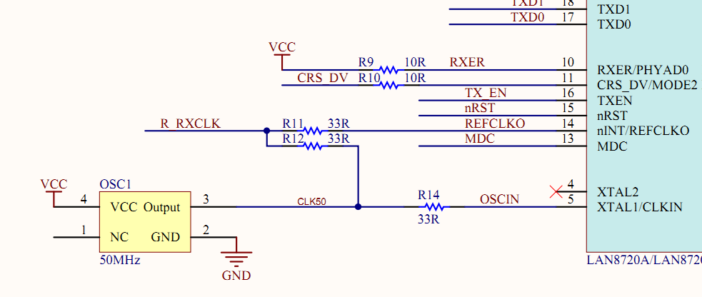
Originally, R12 and R14 were soldered in and R11 left open. In that way the external RXCLK at the pin header and OSCIN to the LAN8720 are both fed with the 50MHz oscillator signal. Pin #14 is configured as nINT but not used at all which makes sense.
I can change my setup to use the second waveshare board with the original configuration. But it shouldn't make much difference. The setup and hold times in figure 5-4 vs. 5-5 are slightly different but all positive and synchronous.
Sounds good. Just need to throw away the oscillator/crystal. The Prop2 will provide the clock.
This is strange. DV / data valid is only high when a packet is received. you would at least see the preamble on the rx0/rx1 pins.
are you sure that tx_en is low? if you send on a half duplex line, CRS might also go up while the line is occupied by the transmitter. (i'm not sure if that really is so)
i would start afresh with the other module. you have done a lot of modding to the pcb which may have caused it to malfunction
That would be a possible explanation. I've checked that TX_EN is really low but that could also be masked by the 1Meg pulldown of the internal resistance of the scope probe. Yes, CRS is active both during transmit and receive when half duplex mode is selected.
This makes no sense as full duplex should have priority if both partners support it.
To be sure that there is no problem with the config straps (pullup/pulldowns) I've also checked the special mode register which contains $60E0. This is the default MODE[2..0] = %111 which enables 10+100M with full duplex and auto-negotiation.
I've also checked that TX_EN is really low with a 10k pullup.
Ok, good news first: with the other board in REF_CLK input mode CRS_DV seems to behave as expected. It is low most of the time and becomes active when packets arrive.
But I had some trouble until this worked. At the beginning the PHY didn't respond to anything and all registers gave $FFFF as read value. I first thought this was because of REGOFF being pulled high by LED1. But the core voltage of 1.2V was present normally. What is strange is that both LEDs are connected to AVDD with the anode (sink mode). The forward voltage of LED1 seems to be high enough to prevent REGOFF from being pulled above the threshold so the regulator is stilll active. But the polarity of the traffic indicator is reversed. The data sheet says it should be connected with the cathode towards ground (see figrure 3-10 right side).
The actual problem was that PHYAD0 was pulled high by R9. I removed R9 and the register were working normally, again.
The special control register still reads $1058 which indicates half duplex according to the data sheet. I'm starting to doubt if the data sheet is correct about that. Maybe they've just mixed up the polarity of bit 4 (full/half duplex) in the description of that register.
BTW, this is the schematic of the Amiga board which has proven to work.
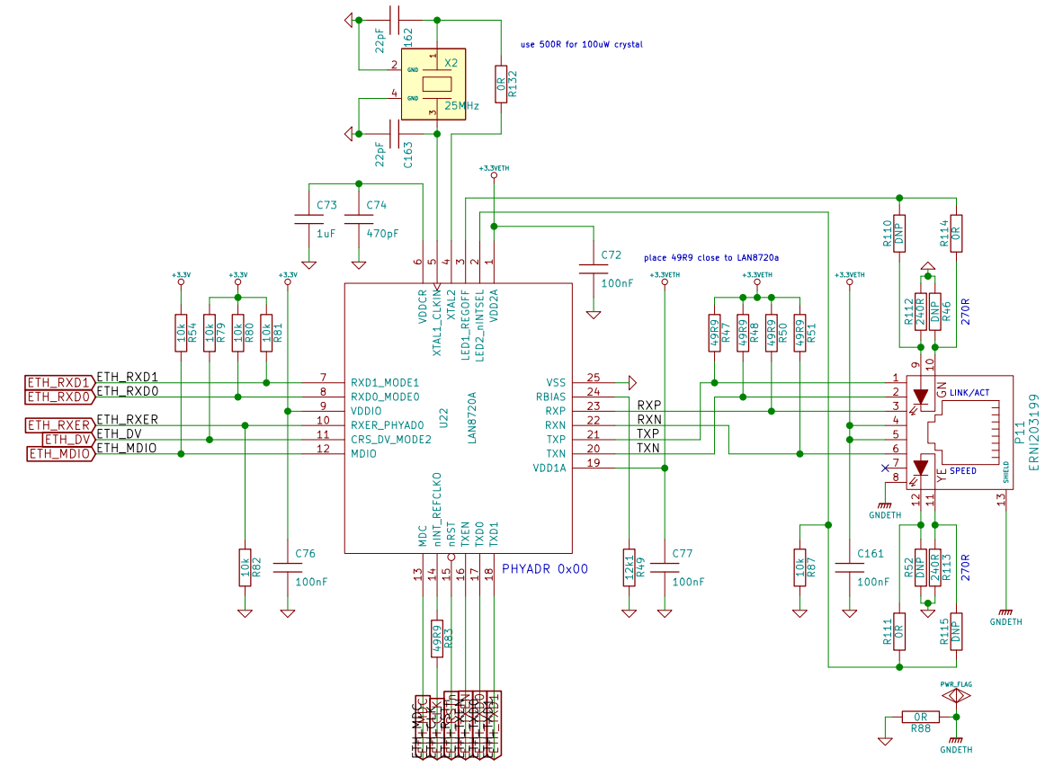
It also pulls REGOFF high with the green LED which is a bad design IMHO but at least works on the eval board. INTSEL is pulled low with R87 which is also bad because the final voltage at LED2/INTSET depends on the forward voltage of the yellow LED which might be close to the threshold voltage of ~1.65V. It even depends on temperature and ambient light (turning it into a PV cell).
Anyway, a 25MHz crystal is connected to XTAL1/2 and REF_CLK is an output driving the clock input of the FPGA on that board. The designer of it told me that he is not writing anything to the configuration registers but fully relies on the configuration strap pins. So we can assume that there is no sprecial trick required to make the REF_CLK output mode work.
Only a thought...
In your setup, I can't see any connection between P2 and nRST, while at the Amiga brd you're referencing, there is a connection to that signal, perhaps towards the FPGA.
Since there are two ways of "forcing" the LAN8720A to recognize the pull-down resistor at LED2/nINTSEL (10K, at the Amiga one) (during power up, or when nRST ends (raising edge)) , which then ensures the configuration of nINT/REFCLKO as a clock output pin, perhaps it's advisable to also control nRST by a P2 pin, as a "second-chance, non-power-cycling"-way of ensureing a sane REFCLKO your setup could rely upon.
The hardware config straps are only sampled on a power on reset. You can trigger a "soft" reset at any time later by writing a 1 to the soft reset bit of the control register but that doesn't re-sample the config strap pins. If you want to change the configuration after power up you have to write directly to all of the control registers that need changes.
Somonius said he had problems with the pullup/pulldown resistors not doing what was expected. But that problem was solved. I also have verified that the chip is in the correct state by reading the status and mode registers. Only the special control register (adr 31) reports conflicting status info. Now that the rest is working I think it's a typo in the data sheet or a bug.
I still have to find out why CRS_DV behaves differently in REF_CLK input and output mode. Maybe my crystal causes some sort of glitches so that received idle codes are not properly decoded as idle. Prototype setups with lots of jumper wires and no solid ground plane might be sensitive to this...
A REF_CLK input mode is the way to go if we want to be able to clock the chip from a breakout board attached to the P2, which is ideal for experimenting with P2-EVAL and P2 EDGE etc, rather than having to try to sync both the P2 XTAL input and PHY devices off the same external clock. The latter approach might be better suited for a custom board design but it would be nice to have something that others could ultimately use with their P2 boards and cheap LAN8720 boards, like the Waveshare ones (potentially HW modified).
I'm somewhat interested in that 25MHz input mode you mentioned. I imagined you needed to output at 50MHz for RMII and 25MHz was for MII but if we can get by with feeding in 25MHz instead of 50MHz this could be handy too as it allows 50:50 duty cycle clocks with the P2 at 250MHz (a sweet spot for video). Obtaining 50MHz from the P2 is not possible at 50% duty cycle other than when at 100MHz, 200MHz, 300MHz P2 operation, in case a PHY needs its clock like that. I think it's right on the edge of its spec if a 40:60 REFCLK clock is used with the LAN8720A, but it should still be okay.
The streaming in of received data from the PHY to the P2 will be interesting to trigger off the CRS_DV if it is asynchronous to the data. I wonder if you'll need to somehow start the transfer and count the clocks until you see non zero on the RXD pin pair to generate some type of bit offset in memory where the real packet starts, or if there will be time to trigger the streamer once you see the pattern on the pins? At 250MHz operation you do get 5 P2 clocks per RMII bit-pair, but there is a delay inside the P2 before you recognize the pin data from code so I think it'll need to be started ahead of time.
We don't really want to end up with a packet in HUB RAM that is not byte aligned in memory and needs every byte bit shifted to fix. Or maybe instead of the streamer the sync smartpin receive mode for both RXD pins could be used and their bits merged? I think @evanh used something similar for the Winbond FLASH in dual SPI mode. This could get interesting to resolve.
There's a whole chapter (3.7 Configuration Straps) at the LAN8720A/LAN8720AI datasheet/manual (Microchip document DS00002165B), where it clearly states that the configuration straps are sampled only during two scenarios:
Chapter 3.8.5 and subsequent ones also ellaborates about hardware and software Reset, including the following: "During a Hardware Reset, an external clock must be supplied to the XTAL1/CLKIN signal", so, if the clock oscillator circuit is someway a "slow-starting-one", then there is the chance for any/some POR to last less than enough, in order to ensure proper initialization of any internal state-machine.
Perhaps some of the aforementionned functions can also be controlled afterwards, by simple software setups, but the ones tagged as "NASR" (aka, Not Affected by Software Reset) explicitly claim they'll need a POR/Hardware-Reset to be correctly configured.
Bringing out the nRST line from LAN8720 pin 15, also C7 / R16, to pin 13 of the header would be ideal - removing R16. That would allow the Prop2 to control the power up conditions. Namely, have the Prop2 boot up first then start the LAN clock going before releasing nRST.
And that's what makes his setup a synchronous RMII link. Either the Prop2 has to be clocked from the LAN's clock, or the LAN chip has to be clocked from the Prop2's clock.
If you have two clock sources then you're operating asynchronously. I'm assuming the Prop2 still has it's own crystal.
PS: There is ways to separate the clocks and still be synchronous, not unlike full blown DDR interfaces I believe, but neither chip has such.
A double wide breakout would allow for some extra control pins as well as the MDC/MDIO pins, if you used a modded Waveshare board, or if a dedicated PHY breakout board was made to suit the P2 headers. Without MDC/MDIO (not sure if that is wise) you could possibly get by with a single wide breakout with 8 IO pins only if you are happy with fixing the link config with strapping resistors or not knowing the link speed if it gets auto-negotiated. (MODE[2:0]=%111). You also wouldn't be able to control PHY power up as easily without the reset or MDIO signals.
yes, it would mean restarting the streamer mid-flight or repacking the whole packet after your received it (adding a large delay)
i bent my head around it and couldn't think of a way the streamer could do it..... but that doesn't mean it's impossible
yes, that's how i'm doing it. btw, have a look on page one of this thread where i shared my code... you might find it interesting
what i do is start the smartpin as soon as DATA_VALID goes up ... i then look in the bitstream for the first '1' bit which designates the start of frame.. while the smartpin is still running i change the bit-width to whatever value is needed to fill up the smartpin with 16 valid bits (since the smartpin just keeps shifting you can access up to 32 previous bits at any time)
.... as soon as that happens, we are in sync with the frame..... keep an eye on CRS/DV (on some phys you need to throw away every other bit because they mux 2 signals on one pin)
stop the smartpin after DV went low and you are done
since you need to access the smart-pin continuously and do the CRC, this occupies almost one complete COG. the benefit you get is such that you end up with the whole packet on the HUB, do whatever you like with it; and there is minimal delay to it
i am even fantasizing about doing packet processing while the packet is on the line, for high level protocol handling this might be of value..... but that all needs a lot of fine-tuning and writing/debugging tight PASM code that it might be just more convenient to do all the protocol handling on another COG in a SPIN context.... might end up having 1 COG for reception and another for transmission + protocol handling (not sure if i ever want to touch TCP but there are a some protocols you probably want to have on a network (ARP, UDP/IP (DHCP), ICMP (PING))
if you just want to network N propellers through a switch you probably get away with only raw ethernet which is quite trivial to implement when all ethernet addresses are pre-set and known to each node
For streamer start trigger, to pick up incoming data, a few sysclocks of forewarning would be enough I think. The I/O latencies have no impact when all signals are incoming, ie: the latencies are the same all round.
One idea is that you'd only collect the first handful of bits with sync receive smartpin, leaving room for an extra first long in the HUB RAM address. Once you know you are synced up on a nice byte boundary, you fire off the streamer which works in parallel while you have the rest of the COG yourself to continue to compute the incoming CRC in parallel. You also write the first missing long to HUB RAM at some point as well during this process. At the end you'd probably indicate a good/bad packet arrival and packet length in some packet header FIFO structure and only advance the data buffer if the CRC was good.
Yes I will have to take a look....
Possibly the IPChecksum could be accumulated and checked on the fly to offload a second P2 COG from doing this later, assuming there is time for this and different header options don't complicate things too much.
Good News (datasheet @ 5.5.4 and beyound; pgs. 60 thru 62):
Except for the crystal oscillator, wich indeed has a sinusoidal waveform, REF_CLK IN will accept a 35/65 waveform (or 65/35. whichever best fits), thus deriving this clock from a P2 running at 250 MHz (2 + 3) or 350 MHz (3 + 4) will represent no problem.
There are in fact two tables, as is:
As for REF_CLK OUT, the limits are (40/60, or 60/40; wich better fits), but the P2 will not mind receiving it that way, so not any problem at that department either.
P.S. Only to clarify: one doesn't needs both; either P2 provides the REF_CLK IN for the LAN8720A, or it provides REF_CLK OUT for the P2.
P.S. II - Besides out of specs, perhaps that chip can also accept 33/66, under specific circumstances, so a test with 150 MHz (1+2) can led to surprising results...
Thanks for all the feedback and suggestions. Well before we make a final decision about which clocking method is best I first need to get it going somehow. Optimizations are lower priority at the moment. But we can talk about the available options.
There are typically 3 scenarios:
1. a full custom board design, you have all the options and can use a common crystal for PHY and P2
2. a P2 eval board combined with a Waveshare eval board with as little modifications as possible, here you need to live with the 50Mhz oscillator on the Waveshare board and the 20MHz crystal on the P2 board
3. a semi-custom design where the P2 provides the clock for the LAN8720
Although 3 seems to be the most straightforward option there are some pitfalls as Yanomani already mentioned. The P2 doesn't have multiple PLLs to produce a clean low-jitter and 50/50 duty cycle clock output. The restriction to use only multiples of 100MHz as sysclock would result in problems using video and LAN at the same time. So I think option 3 should be dropped.
I think the P2 should be able to synchronize serial bitstreams properly to an external clock even if it runs completely asynchronously. If the sysclock is well above 100MHz (or above 125MHz for a worst case of 40/60 duty at 50MHz) then it's guaranteed that high and low phases of the 50MHz clock will be reliably sampled. Of course, we can't use the streamer then.
I plan to make two versions of the driver. One universal verseion that uses two cogs, supports full duplex and clocking options 1 and 2. A "reduced resources" version could be implemented later which only uses one cog and only works with clock option 1 and half duplex. The streamer could be used to transmit packets and smart pin in synchronous serial receive mode to receive them. There is no plan to use the streamer for receiving as this would be really hard to implement (see Simonius' explanation about synchronizing the start-of-frame in post #53).
Thanks for the explanation. I also thought hard about how to synchronize to the start-of-frame. Unfortunatelly, the bit that distinguishes the SSD from the preamble ($D5 vs. $55) is the last one. So there won't be any time to adjust the shift register before the first bit pair of the header (destination address) comes in. But if it can be done during the preamble by looking for the first '1' then it should be easy. Interesting to know that the bit-width of the SYNC_RX smart pin can be changed on the fly. Very helpful hint. I already looked at your code but haven't fully understood what is going on there.

I do still like the idea of your third scenario, i.e. P2 outputting the clock to the LAN8720 despite the clock limitations because then you can potentially stream synchronously in and out with very low COG overheads, freeing it to do other useful things such as CRC on the fly. Even though it is tricky I think there would be a way to make it work, but I'd need to experiment too to prove this to myself. Ultimately I've had a lot of success with the streamer in similar complex timing situations with my different drivers so maybe I'm becoming too overconfident.... The P2 would need to run at 100, 200, 250, 300MHz, unless the 25MHz clocking via XTAL in on the PHY also works out and the chip's 50MHz clock output still remains synced to the P2, so this is a fairly significant operational constraint. Another downside is you do need to mod the cheap Waveshare board to get the clock path working this way (a simple mod), unless you build a dedicated P2 breakout board with the PHY directly populated on it and which also connects this clock signal directly from the P2. That would probably need to be done if MDC and MDIO are also desired anyway. But who would be making this board, and how high a cost would it be vs the very cheap Waveshare option?
If it is possible to get all wire speed functionality working with the second scenario with 2 COGs that could actually be good too, though I'm not sure if you'll have time for the CRC calculation on the fly at lower P2 clock speeds (hopefully I'm proven wrong there - I still have to read Simonius code to see). That could limit sustained transmit speeds if it has to be computed beforehand or may need additional COG resources to check afterwards. You'd want to be confident in the minimum clock speed requirements for this approach, but having the flexibility to run the P2 above some minimum rate and still keep Ethernet working is very handy, especially in situations where video is using various clock speeds.
Here is some code inside the spoiler section:
If i counted correctly, these are the minimal sequence of 19 Instructions to deal with 32 bits worth of network data... there will be some more overhead that i didn't show but that's basically it!
Simonius's solution is fine. As long as sysclock is fast enough, the smartpin can track the clock and thereby identify where the data bits are. Needs maybe 5x the data rate. Streamer can't do that, it blindly samples the I/O. Don't even bother with any streamer code until there is a common sysclock for both chips.
As for all the other excuses about timings, like conflicting with video rates, every one of them is bogus. Monitors/TVs are very flexible with dot clocks. Prop2 can produce 50:50 square clock no problem.