So roughly 38 P2 clocks to deal with 16 clocked bit pairs (32 bits) of data arriving at 50MHz. That would indicate you need 38 P2 clocks every 16/50M = 320ns. This means you need at least 38M*3.125 P2 clks/s ~ 118MHz to keep up. Let's say maybe >140MHz to be sure with more headroom left for overheads to manage ending conditions, buffer addresses and packet length stuff etc.
If we believe the nyquist theorem we get away with a little more than 100 MHz to sample the 50 MHz clock. I can bring down the minimal frequency a bit by shaving off an instruction or two from the main loop. i have not tested what is actually the lower limit right now
BTW, I like what you've done with leaving the CRS pin as plain IN bit. I was looking at the WRPINs and thinking why is the clock pin got its smartA input reaching over to CRS and then it dawned on me that that allows CRS to function as both IN and a smartpin. Good trick. I'm so used to the clock pin being an output and using the pulse gen smartpin mode.
Pertaining to sample rate: RMII specifies a data setup of 4 ns and data hold of 2 ns. So 6 ns combined. 200 MHz is 5 ns sampling interval, I really wouldn't want to be longer than that.
Reading the LAN8720 datasheet it looks most likely that the rx data pins are clocked out on the low going edge. So I see why you've adjust the rx data smartpins to capture the sample on the post-rising clock rather than pre-rising. Amusingly, though, it only guarantees 3 ns hold time from clock rise.
Don't worry about the minimum P2 clock. Nobody runs the P2 lower than 175MHz unless there is a reason, for example saving power in a battery powered sytem.
The RMII data pins are also not the problem. Data becomes valid after the rising edge of REF_CLK. Look at the toval spec (figure 5-5, table 5-10). In the REF_CLK input mode it's nominally less than 14ns which means the setup time to the next clock edge is 6ns, In REF_CLK output mode the spec is much better, toval < 5ns or setup time >15ns, theoretically.
In practice toval is actually around 5ns. I've checked this with the scope. That's good in the final application as it provides plenty of margin. But for debugging the software it's bad because it masks possible problems. the RX data might look good although the timing is way off.
I'm thinking Streamer byte ordering isn't a concern either. It'll place bytes into hubRAM in the same order as they arrive in the packets. Whatever the sender sends is what you get. Of course, Internet Protocol is explicitly big-endian, but that's a problem for a higher layer of processing.
@ManAtWork said:
In practice toval is actually around 5ns. I've checked this with the scope.
Good. The 14 ns value was just ridiculous. There was no way that could ever be reasonable. Okay, that means the rx data sampling setting for post-rise sampling isn't ideal then.
Change this
WXPIN #%1_01111 , #pin_CLK + (2 << 6) 'from now on always fetch 16(*2) bits
to this
WXPIN #%0_01111 , #pin_CLK + (2 << 6) 'from now on always fetch 16(*2) bits
and this
WXPIN #%1_00111 , #pin_CLK + (2 << 6) 'set data width to 8 bit for CLK, RX0, RX1
to this
WXPIN #%0_00111 , #pin_CLK + (2 << 6) 'set data width to 8 bit for CLK, RX0, RX1
@evanh said:
Okay, that means the rx data sampling setting for post-rise sampling isn't ideal then.
Good point. I was also worried about how to verify that the sampling timing is correct. For an output signal you can have a look with the scope and see if the timing is right. But for an input signal you don't see when the actual sampling takes place. Well, unless it's so off that the data gets corrupted.
A possible solution would be to delay the data line until the samples get invalid. Then delay the clock until the data again becomes invalid. And then choose the center of the tolerance band. In the smart pin low level settings there is an option to use "clocked logic" which would delay the input for one clock. The digital filters can be used for delays of more than one clock. I've already used this in the LCD driver to fine-adjust the timing.
Won't help ... Shifting the data capture point further away from the serial clock edge isn't gaining anything ... It's just a question of does the smartpin use the data pin level of one sysclock prior to discovery of serial clock rise (pre-rise) or the data pin level at serial clock rise discovery (post-rise).
Making all RMII pins registered would tidy up the small differences in I/O propagation. It's not of any real significance but may as well flick them on, they're a freebie.
@evanh said:
Won't help ... Shifting the data capture point further away from the serial clock edge isn't gaining anything ...
You probably misunderstood me. Of course, if the signal quality is bad, i.e. the window in the eye-diagram is too narrow then shifting the sampe point won't help. But if the signal quality is "too good" meaning that the result looks good but you don't know if it's just good luck and it won't fail with a different chip at a different temperature then doing a "monte carlo" test is a good idea. If you checked that it still works for both cases, the clock delayd or the data delayed by one clock, then you can be sure that you're not close too the edge but have at least one sysclock margin in both directions.
What LCD has data coming back to the Prop2?
None. But you can also use the filters to fine tune the timing of the data outputs to the clock. The clock is generated by a smart pin but is re-sampled at the input of the SYNC_TX smart pin. So it's always late.
@ManAtWork said:
... then you can be sure that you're not close too the edge but have at least one sysclock margin in both directions.
Bad idea for a synchronous stream like this. But I guess it can confirm there isn't a mistake in understanding.
What LCD has data coming back to the Prop2?
None. But you can also use the filters to fine tune the timing of the data outputs to the clock. The clock is generated by a smart pin but is re-sampled at the input of the SYNC_TX smart pin. So it's always late.
Hmm ... making the data output even later than it already is ... dunno about that.
X[5] = 0 selects the A input sample just before the B input edge was registered. This requires no hold time on the part of the
sender.
X[5] = 1 selects the sample coincident with the B edge being registered. This is useful where transmitted data remains steady after
the B edge for a brief time.
Yipeee! I can receive the preamble. When I read the first 32 received bits after CRS goes high I get either a $55555500 or a $55555400. LSB come in first so this means I sometimes get 4 and sometimes 5 zero bit pairs before the first valid data of the preamble.
Well that's actually no miracle especially after Simonius posted his code that was able to do this long before. But I want to understand every step.
Hmm, I've checked that with the scope. The preamble or whatever that is, a series of bit pairs with RXD0 constantly high and RXD1 constantly low ($5555...) is lasting for something around 600ns. That are 30 clocks of 50MHz or 60 bits altogether.
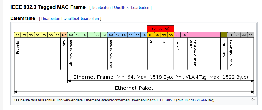
I hate it when the data sheets do not tell the truth... From figure 3-3 I thought I should see a $55 for the decoded J+K symbols and then a $555D for the preamble and start of frame delimiter. Ok, they shrinked that to save space. Wkipedia says that the preamble has 7 bytes and the SFD one byte. That would be 8 bytes or 64 bits alltogether. Makes sense
@ManAtWork said:
Yipeee! I can receive the preamble.
Good work.
When I read the first 32 received bits after CRS goes high I get either a $55555500 or a $55555400. LSB come in first so this means I sometimes get 4 and sometimes 5 zero bit pairs before the first valid data of the preamble.
Well that's actually no miracle especially after Simonius posted his code that was able to do this long before. But I want to understand every step.
Wait... shouldn't it be $D5555500 and $55555400 ?
You might be missing the last nibble if the smartpin started off capturing old pin data in the P2 pipeline. I think you need to delay the capture by another nibble worth or more to see it here. ie. if you captured another 4 bits you'd see the "D" (1101 pattern),
@Simonius said:
you could also use the MDIO for setup. one of the RX pins and MDIO could be tied together to save one pin, this way one phy could be connected on a single 2x6 header of the prototype board
Sorry to bring up an earlier point, as I came in late and missed following a lot of the early discussion and am only now beginning to catch up here - (lot of gold being found in Simonius' work).
I am intrigued by this idea of fitting the PHY to an 8 pin P2 group only while also retaining SMI control with MDC/MDIO signals. So @Simonius, in your statement above, were you meaning sharing MDIO with an RX pin on the P2, or an RX pin on the PHY? I could see a possible way if you have a separately controlled MDC pin that is stopped during normal Ethernet transmissions (TXEN=1), and you share a TX pin from the P2 which can be made to read write MDIO data to setup PHY registers at the same time as you drive the MDC signal.
E.g. just wire up these 8 pins:
TXD0 + MDIO (MDIO output and pin gets turned around to become an input when SMI is reading a PHY register)
TXD1
TX_EN
MDC (only ever activated when TX_EN = 0 and you want to do an SMIO transfer)
RXD0
RXD1
CRS_DV
REF_CLK
Yes, RX_ER could be disconnected if the RX code can depend on CRC only to determine errors.
TXD0 + MDIO (MDIO output and pin gets turned around to become an input when SMI is reading a PHY register)
MDC (only ever activated when TX_EN = 0 and you want to do an SMIO transfer)
Yes, that is what i meant. I was thinking that unless you use this Serial Management Interface a lot, it could as well share one pin with the TX interface
since the serial interface is slow (the datasheet says one bit-time is 400 ns) it's admittedly occupying the TX line for quite some time.
i have not yet used the SMI yet i still rely on the hardwired setup (AUTO 10/100 MBIT, full-duplex)
Yes, RX_ER could be disconnected if the RX code can depend on CRC only to determine errors.
I thought so. @ManAtWork objected that in a noisy industrial environment this technique would introduce false positive errors since the CRC is only 32 bit and if there a lot of multiple-bit errors then it's just a matter of time until you get a matching CRC for a broken packet
I am not sure if the PHY would in this case detect those errors... and if it did, i read somewhere that some PHYs corrupt the CRC deliberately to mark the packet incorrect... a clever solution
I am intrigued by this idea of fitting the PHY to an 8 pin P2 group only while also retaining SMI control with MDC/MDIO signals.
that is exacly what i thought. it would make for a good P2 module... until the parallax shop has those, just use the waveshare boards and build your own custom 2x7 to 2x6 adapter cable suited cablesand matching housings
TXD0 + MDIO (MDIO output and pin gets turned around to become an input when SMI is reading a PHY register)
MDC (only ever activated when TX_EN = 0 and you want to do an SMIO transfer)
Yes, that is what i meant. I was thinking that unless you use this Serial Management Interface a lot, it could as well share one pin with the TX interface
since the serial interface is slow (the datasheet says one bit-time is 400 ns) it's admittedly occupying the TX line for quite some time.
It would not be an issue for initial setup use and PHY reset etc. It's only an issue really if you intended to poll the PHY registers (eg. for stats) regularly and didn't want to delay transmission during this time.
Yes, RX_ER could be disconnected if the RX code can depend on CRC only to determine errors.
I thought so. @ManAtWork objected that in a noisy industrial environment this technique would introduce false positive errors since the CRC is only 32 bit and if there a lot of multiple-bit errors then it's just a matter of time until you get a matching CRC for a broken packet
I am not sure if the PHY would in this case detect those errors... and if it did, i read somewhere that some PHYs corrupt the CRC deliberately to mark the packet incorrect... a clever solution
Ok. Yeah well it would be possible to miss some PHY errors if the CRC randomly still matches. I think it would be prudent to write a driver that could either work with or without this RX_ER signal, depending on startup configuration flags etc. Some people might be happy to run without to save pins and work with a simple 8 pin breakout adapter for home use etc, but some people might want the full error handling in the reconciliation sublayer (before the MAC and after the PHY), and that requires interpretation of the RX_ER signal (and a modification of the Waveshare board).
EDIT: And ManAtWork has measured that the LAN8720A is holding data for about 5 ns post-clock. Which is barely enough to cover the sampling interval. There is far more setup pre-clock available. And on that note, even the RMII spec has greater minimum setup (4 ns) than hold (2 ns). https://forums.parallax.com/discussion/comment/1535417/#Comment_1535417
Good news: I can synchronize to the SFD, receive real packet data and also calculate the length of the packet. Simonius' trick to monitor the real time state of the CRS_DV signal with the +/-3 pins re-routing over the REFCLK pin was very helpful. I've first tried to switch the CRS_DV pin from normal input mode (to detect the rising edge immediately) to smart mode (to synchronously sample it during data reception) and back. But that was complicated and led to misaligned samples.
I still have some problems using the event system to detect the inter-frame gap especially after errors. CRS_DV could toggle at 25MHz at the end of a packet and there could be false alarms when there is noise on an idle line which results in short pulses. So I think it would be a good idea to wait until CRS_DV is completely inactive for at least the duration of the minimum inter-frame gap before the event trigger on a rising edge is armed again.
There must be some filter functions in the pins to do denoising/debouncing. i have not yet tried them.
the inter frame gap is set in the standard but i guess many switches will also forward packets with a lower gap and also packets smaller than the minimal length which might lead to much lower latencies
The so called "digital filters" in the input pins are good for de-bouncing. But the introduce some unknown delay because for longer periods than just a few clocks they run from a clock divider. So it's hard to know the exact sample points.
The idea is to create a retriggerable timer. If a rising edge on Crs is detected the timer re-starts. If it times out then the gap is detected and the next rising edge triggers a packet receive attempt. But it doesn't work. After the first packet is received it waits forever. The event to start receiving data works so it's not the SETSE that's wrong. It also works if I comment out the 'if_nc...' line. That shows that the timeout also works.
@ManAtWork said:
The so called "digital filters" in the input pins are good for de-bouncing. But the introduce some unknown delay because for longer periods than just a few clocks they run from a clock divider. So it's hard to know the exact sample points.
Just a minor observation that may help you find the right sweetspot, in order to leverage from the digital filters for smart pins:
the so called "timing taps" are, in fact, the equivalents bit positions at CT (0, 5, 19 or 22), so, by grabbing it beforehand (GET CT (without WC)), masking unuseful lower bits, and adding a suitable target offset while configuring the desired HUBSET command will enable your filtering routine to find the right spot for the first sampling period, and keep in deterministic sync, thereon.
This is not exactly easy at the lowermost sampling tap (aka "0"), but you can use the timming to your advantege, starting from a higher one (5, 19 or 22 (whichever best fits your needs)), just to be sure you arrive in sync, at the right spot, from the very beggining.
At the end, is just the "old good habit of counting clock cycles" for each instruction, but if it was not that way, what's the reason for using assembly???
For sure, there are interrupts and events that can be used atto your advantage, as a means of achieving the best compromise between your needs, and code complexity.
Hope it helps a bit
Henrique
Important clarification/correction:
the filter lenghts spans two bits, thus only contemplate four hardware pre-set options, as follows:
lenght field number of flipflops
00 2
01 3
10 5
11 8
as for the tap field, wich spans five bits, it's fully programable, in order to enable choosing each and every of the 32 possible bit-positions of CT (low); the options configured as defaults, on reset, can be changed at any time.
tap field CT (low) bit
00000 00
00001 01
.......... ....
11111 31
@ManAtWork said:
Good news: I can synchronize to the SFD, receive real packet data and also calculate the length of the packet. Simonius' trick to monitor the real time state of the CRS_DV signal with the +/-3 pins re-routing over the REFCLK pin was very helpful. I've first tried to switch the CRS_DV pin from normal input mode (to detect the rising edge immediately) to smart mode (to synchronously sample it during data reception) and back. But that was complicated and led to misaligned samples.
>
Well done.
I still have some problems using the event system to detect the inter-frame gap especially after errors. CRS_DV could toggle at 25MHz at the end of a packet and there could be false alarms when there is noise on an idle line which results in short pulses. So I think it would be a good idea to wait until CRS_DV is completely inactive for at least the duration of the minimum inter-frame gap before the event trigger on a rising edge is armed again.
I think this is a good idea. That CRS_DV signal oscillation worried me as well when I first read about it given it is critical to the operation of delineating packets. An IPG quiet time state requirement should help sort it out. You might also get this false carrier event mentioned in the datasheet, so your initial decoding state might have to timeout if it doesn't see the SFD in time.
Yes, this is exactly what I've planned to do. If the SFD is not recognized within the first 96 bits OR if CRS becomes low during that time OR if RX_ER becomes high anytime during the whole packet transmission then I jump to the "wait-for-IPG" procedure. I just have to debug it.
I think I have read somewhere that the minimum inter-frame gap is 96 bits or 960ns for the original sender of the packet. But it can become shorter when the data travels over multiple hops with slightly different clock frequencies. It can become as low as 36 bits or 360ns in a worst case scenario.
BTW that number 96 if my SFD timeout has nothing to do with the IPG time. It's just a consequence of the fact that I sample 32 bits right after CRS goes high and then a variable number of 32..64 bits for synchronisation.
I think I have read somewhere that the minimum inter-frame gap is 96 bits or 960ns for the original sender of the packet. But it can become shorter when the data travels over multiple hops with slightly different clock frequencies. It can become as low as 36 bits or 360ns in a worst case scenario.
Am not sure about that much slip in a normal Ethernet environment, it would be outrageously bad crystal frequency mismatch between ends to cause a difference of 60 bits in a large 1518 byte packet (1538 bits on the wire with preamble and IPG). To slip this number of bits would require a frequency difference of 60/(1538*8) = 4876ppm. This is seriously bad tolerance. I recall a rule of thumb was that +/-50ppm xtals were needed for Ethernet. Maybe a 64kB jumbogram could just about slip that much though if one end was clocking out at 50ppm high and the other end was clocking in at 50ppm too low...


Comments
So roughly 38 P2 clocks to deal with 16 clocked bit pairs (32 bits) of data arriving at 50MHz. That would indicate you need 38 P2 clocks every 16/50M = 320ns. This means you need at least 38M*3.125 P2 clks/s ~ 118MHz to keep up. Let's say maybe >140MHz to be sure with more headroom left for overheads to manage ending conditions, buffer addresses and packet length stuff etc.
I'd want 250 MHz just for good sampling clearance of the smartpin inputs. And I see Simonius is already up there at 230 MHz.
If we believe the nyquist theorem we get away with a little more than 100 MHz to sample the 50 MHz clock. I can bring down the minimal frequency a bit by shaving off an instruction or two from the main loop. i have not tested what is actually the lower limit right now
Unwise, but yeah, lower does still work.
BTW, I like what you've done with leaving the CRS pin as plain IN bit. I was looking at the WRPINs and thinking why is the clock pin got its smartA input reaching over to CRS and then it dawned on me that that allows CRS to function as both IN and a smartpin. Good trick. I'm so used to the clock pin being an output and using the pulse gen smartpin mode.
Pertaining to sample rate: RMII specifies a data setup of 4 ns and data hold of 2 ns. So 6 ns combined. 200 MHz is 5 ns sampling interval, I really wouldn't want to be longer than that.
Reading the LAN8720 datasheet it looks most likely that the rx data pins are clocked out on the low going edge. So I see why you've adjust the rx data smartpins to capture the sample on the post-rising clock rather than pre-rising. Amusingly, though, it only guarantees 3 ns hold time from clock rise.
Don't worry about the minimum P2 clock. Nobody runs the P2 lower than 175MHz unless there is a reason, for example saving power in a battery powered sytem.
The RMII data pins are also not the problem. Data becomes valid after the rising edge of REF_CLK. Look at the toval spec (figure 5-5, table 5-10). In the REF_CLK input mode it's nominally less than 14ns which means the setup time to the next clock edge is 6ns, In REF_CLK output mode the spec is much better, toval < 5ns or setup time >15ns, theoretically.
In practice toval is actually around 5ns. I've checked this with the scope. That's good in the final application as it provides plenty of margin. But for debugging the software it's bad because it masks possible problems. the RX data might look good although the timing is way off.
Anyway, 200 MHz or more should be fine.
I'm thinking Streamer byte ordering isn't a concern either. It'll place bytes into hubRAM in the same order as they arrive in the packets. Whatever the sender sends is what you get. Of course, Internet Protocol is explicitly big-endian, but that's a problem for a higher layer of processing.
Good. The 14 ns value was just ridiculous. There was no way that could ever be reasonable. Okay, that means the rx data sampling setting for post-rise sampling isn't ideal then.
Change this
to this
and this
to this
Good point. I was also worried about how to verify that the sampling timing is correct. For an output signal you can have a look with the scope and see if the timing is right. But for an input signal you don't see when the actual sampling takes place. Well, unless it's so off that the data gets corrupted.
A possible solution would be to delay the data line until the samples get invalid. Then delay the clock until the data again becomes invalid. And then choose the center of the tolerance band. In the smart pin low level settings there is an option to use "clocked logic" which would delay the input for one clock. The digital filters can be used for delays of more than one clock. I've already used this in the LCD driver to fine-adjust the timing.
Won't help ... Shifting the data capture point further away from the serial clock edge isn't gaining anything ... It's just a question of does the smartpin use the data pin level of one sysclock prior to discovery of serial clock rise (pre-rise) or the data pin level at serial clock rise discovery (post-rise).
Making all RMII pins registered would tidy up the small differences in I/O propagation. It's not of any real significance but may as well flick them on, they're a freebie.
What LCD has data coming back to the Prop2?
You probably misunderstood me. Of course, if the signal quality is bad, i.e. the window in the eye-diagram is too narrow then shifting the sampe point won't help. But if the signal quality is "too good" meaning that the result looks good but you don't know if it's just good luck and it won't fail with a different chip at a different temperature then doing a "monte carlo" test is a good idea. If you checked that it still works for both cases, the clock delayd or the data delayed by one clock, then you can be sure that you're not close too the edge but have at least one sysclock margin in both directions.
None. But you can also use the filters to fine tune the timing of the data outputs to the clock. The clock is generated by a smart pin but is re-sampled at the input of the SYNC_TX smart pin. So it's always late.
Bad idea for a synchronous stream like this. But I guess it can confirm there isn't a mistake in understanding.
Hmm ... making the data output even later than it already is ... dunno about that.
i am not convinced yet why this would be right. can you please elaborate on that a bit?
X[5] = 0 selects the A input sample just before the B input edge was registered. This requires no hold time on the part of the
sender.
X[5] = 1 selects the sample coincident with the B edge being registered. This is useful where transmitted data remains steady after
the B edge for a brief time.
Yipeee!") I can receive the preamble. When I read the first 32 received bits after CRS goes high I get either a $55555500 or a $55555400. LSB come in first so this means I sometimes get 4 and sometimes 5 zero bit pairs before the first valid data of the preamble.
I can receive the preamble. When I read the first 32 received bits after CRS goes high I get either a $55555500 or a $55555400. LSB come in first so this means I sometimes get 4 and sometimes 5 zero bit pairs before the first valid data of the preamble.
Well that's actually no miracle especially after Simonius posted his code that was able to do this long before. But I want to understand every step.
Wait... shouldn't it be $D5555500 and $55555400 ?
Hmm, I've checked that with the scope. The preamble or whatever that is, a series of bit pairs with RXD0 constantly high and RXD1 constantly low ($5555...) is lasting for something around 600ns. That are 30 clocks of 50MHz or 60 bits altogether.
I hate it when the data sheets do not tell the truth... From figure 3-3 I thought I should see a $55 for the decoded J+K symbols and then a $555D for the preamble and start of frame delimiter. Ok, they shrinked that to save space.
  Wkipedia says that the preamble has 7 bytes and the SFD one byte. That would be 8 bytes or 64 bits alltogether. Makes sense
I have printet this out and nailed it to the wall behind my monitor just in the case I forget it.")
Good work.
You might be missing the last nibble if the smartpin started off capturing old pin data in the P2 pipeline. I think you need to delay the capture by another nibble worth or more to see it here. ie. if you captured another 4 bits you'd see the "D" (1101 pattern),
Sorry to bring up an earlier point, as I came in late and missed following a lot of the early discussion and am only now beginning to catch up here - (lot of gold being found in Simonius' work).
I am intrigued by this idea of fitting the PHY to an 8 pin P2 group only while also retaining SMI control with MDC/MDIO signals. So @Simonius, in your statement above, were you meaning sharing MDIO with an RX pin on the P2, or an RX pin on the PHY? I could see a possible way if you have a separately controlled MDC pin that is stopped during normal Ethernet transmissions (TXEN=1), and you share a TX pin from the P2 which can be made to read write MDIO data to setup PHY registers at the same time as you drive the MDC signal.
E.g. just wire up these 8 pins:
Yes, RX_ER could be disconnected if the RX code can depend on CRC only to determine errors.
Yes, that is what i meant. I was thinking that unless you use this Serial Management Interface a lot, it could as well share one pin with the TX interface") i still rely on the hardwired setup (AUTO 10/100 MBIT, full-duplex)
i still rely on the hardwired setup (AUTO 10/100 MBIT, full-duplex)
since the serial interface is slow (the datasheet says one bit-time is 400 ns) it's admittedly occupying the TX line for quite some time.
i have not yet used the SMI yet
I thought so. @ManAtWork objected that in a noisy industrial environment this technique would introduce false positive errors since the CRC is only 32 bit and if there a lot of multiple-bit errors then it's just a matter of time until you get a matching CRC for a broken packet
I am not sure if the PHY would in this case detect those errors... and if it did, i read somewhere that some PHYs corrupt the CRC deliberately to mark the packet incorrect... a clever solution
that is exacly what i thought. it would make for a good P2 module... until the parallax shop has those, just use the waveshare boards and build your own custom 2x7 to 2x6 adapter cable suited cables and matching housings
It would not be an issue for initial setup use and PHY reset etc. It's only an issue really if you intended to poll the PHY registers (eg. for stats) regularly and didn't want to delay transmission during this time.
Ok. Yeah well it would be possible to miss some PHY errors if the CRC randomly still matches. I think it would be prudent to write a driver that could either work with or without this RX_ER signal, depending on startup configuration flags etc. Some people might be happy to run without to save pins and work with a simple 8 pin breakout adapter for home use etc, but some people might want the full error handling in the reconciliation sublayer (before the MAC and after the PHY), and that requires interpretation of the RX_ER signal (and a modification of the Waveshare board).
Read this - https://forums.parallax.com/discussion/comment/1535429/#Comment_1535429
EDIT: And ManAtWork has measured that the LAN8720A is holding data for about 5 ns post-clock. Which is barely enough to cover the sampling interval. There is far more setup pre-clock available. And on that note, even the RMII spec has greater minimum setup (4 ns) than hold (2 ns). https://forums.parallax.com/discussion/comment/1535417/#Comment_1535417
Good news: I can synchronize to the SFD, receive real packet data and also calculate the length of the packet. Simonius' trick to monitor the real time state of the CRS_DV signal with the +/-3 pins re-routing over the REFCLK pin was very helpful. I've first tried to switch the CRS_DV pin from normal input mode (to detect the rising edge immediately) to smart mode (to synchronously sample it during data reception) and back. But that was complicated and led to misaligned samples.
I still have some problems using the event system to detect the inter-frame gap especially after errors. CRS_DV could toggle at 25MHz at the end of a packet and there could be false alarms when there is noise on an idle line which results in short pulses. So I think it would be a good idea to wait until CRS_DV is completely inactive for at least the duration of the minimum inter-frame gap before the event trigger on a rising edge is armed again.
There must be some filter functions in the pins to do denoising/debouncing. i have not yet tried them.
the inter frame gap is set in the standard but i guess many switches will also forward packets with a lower gap and also packets smaller than the minimal length which might lead to much lower latencies
The so called "digital filters" in the input pins are good for de-bouncing. But the introduce some unknown delay because for longer periods than just a few clocks they run from a clock divider. So it's hard to know the exact sample points.
In my code I currently use this:
              mov     tmp,#%001<<6
              or      tmp,pinCrsDv
              setse1  tmp                       ' CRS rising edge
...
              pollse1
waitIpg       setq    timeMinIpg
              waitse1 wc                        ' wait min inter-packet gap, C=timeout
        if_nc jmp     #waitIpg                  ' repeat if CRS=1 detected (not idle)
              jmp     #rxMainLoop
The idea is to create a retriggerable timer. If a rising edge on Crs is detected the timer re-starts. If it times out then the gap is detected and the next rising edge triggers a packet receive attempt. But it doesn't work. After the first packet is received it waits forever. The event to start receiving data works so it's not the SETSE that's wrong. It also works if I comment out the 'if_nc...' line. That shows that the timeout also works.
Just a minor observation that may help you find the right sweetspot, in order to leverage from the digital filters for smart pins:
This is not exactly easy at the lowermost sampling tap (aka "0"), but you can use the timming to your advantege, starting from a higher one (5, 19 or 22 (whichever best fits your needs)), just to be sure you arrive in sync, at the right spot, from the very beggining.
At the end, is just the "old good habit of counting clock cycles" for each instruction, but if it was not that way, what's the reason for using assembly???
For sure, there are interrupts and events that can be used at to your advantage, as a means of achieving the best compromise between your needs, and code complexity.
Hope it helps a bit
Henrique
Important clarification/correction:
lenght field number of flipflops 00 2 01 3 10 5 11 8Sorry for my mistaken readout of the docs...
>
Well done.
I think this is a good idea. That CRS_DV signal oscillation worried me as well when I first read about it given it is critical to the operation of delineating packets. An IPG quiet time state requirement should help sort it out. You might also get this false carrier event mentioned in the datasheet, so your initial decoding state might have to timeout if it doesn't see the SFD in time.
Yes, this is exactly what I've planned to do. If the SFD is not recognized within the first 96 bits OR if CRS becomes low during that time OR if RX_ER becomes high anytime during the whole packet transmission then I jump to the "wait-for-IPG" procedure. I just have to debug it.
I think I have read somewhere that the minimum inter-frame gap is 96 bits or 960ns for the original sender of the packet. But it can become shorter when the data travels over multiple hops with slightly different clock frequencies. It can become as low as 36 bits or 360ns in a worst case scenario.
BTW that number 96 if my SFD timeout has nothing to do with the IPG time. It's just a consequence of the fact that I sample 32 bits right after CRS goes high and then a variable number of 32..64 bits for synchronisation.
Am not sure about that much slip in a normal Ethernet environment, it would be outrageously bad crystal frequency mismatch between ends to cause a difference of 60 bits in a large 1518 byte packet (1538 bits on the wire with preamble and IPG). To slip this number of bits would require a frequency difference of 60/(1538*8) = 4876ppm. This is seriously bad tolerance. I recall a rule of thumb was that +/-50ppm xtals were needed for Ethernet. Maybe a 64kB jumbogram could just about slip that much though if one end was clocking out at 50ppm high and the other end was clocking in at 50ppm too low...