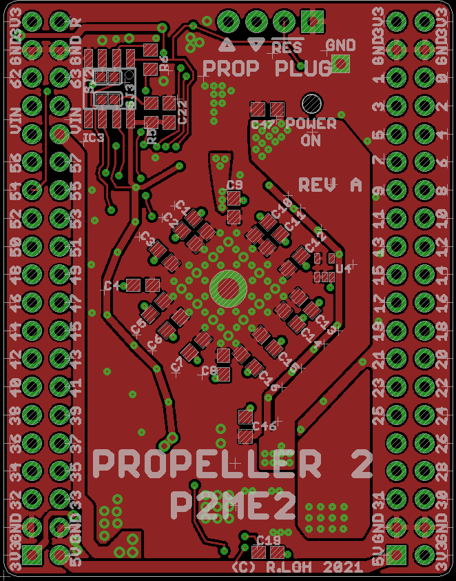
I think it is very important to place the bypass caps as close as possible to the P2. Even a short trace of only 1/2 or 1/4 inch makes a inductance of a few nH which forms a series resonant tank together with the cap and renders it useless for high frequencies. C26, C27 and some others are too far away, in my opinion.
I know that can be too late for a warning, and also no one know that pcb better than you, but would you mind putting some references for JP1/JP2, at least at the silk screen masks, perhaps near their "Pin 1" designations.
Since you've provided the Prop Plug "Pin 1" with a nice square pad identifier, perhaps it would also be good to have the same ID at JP1 and JP2, but this would demmand more that a little editing to settle.
Sorry for the late comment, but I was out almost the whole morning, so only saw your last designs just about now.
@ManAtWork said:
I think it is very important to place the bypass caps as close as possible to the P2. Even a short trace of only 1/2 or 1/4 inch makes a inductance of a few nH which forms a series resonant tank together with the cap and renders it useless for high frequencies. C26, C27 and some others are too far away, in my opinion.
Yes, I found it's a bit of challenge to get the VCCIO bypass caps all close without chopping off the wide ground current path for good heat spread on a two layer board. A two layer board is going to be a bit of a compromise there. I'll continue on a rev B version today to try to squeeze them a little closer and see if there is a little more time today to try to get that version used.
@Yanomani said:
Hi rogloh
I know that can be too late for a warning, and also no one know that pcb better than you, but would you mind putting some references for JP1/JP2, at least at the silk screen masks, perhaps near their "Pin 1" designations.
Since you've provided the Prop Plug "Pin 1" with a nice square pad identifier, perhaps it would also be good to have the same ID at JP1 and JP2, but this would demmand more that a little editing to settle.
Sorry for the late comment, but I was out almost the whole morning, so only saw your last designs just about now.
Henrique
No worries. Looks like I had missed that lack of a square pad in the part I placed. Normally the pin 1 pad is square on headers but is not in this part I grabbed from some random library. Yeah I should try to identify it. There are JP1 and JP2 labels down on the bottom layer but pin 1 is not properly identified.
While I'm at it I probably should add P2 pin number labels down the side. But I really don't want this to turn into a full blown P2D2. My P2ME2 is a poor man's P2D2. The "Clayton's" P2D2 if you like. https://en.wiktionary.org/wiki/Claytons
There are JP1 and JP2 labels down on the bottom layer but pin 1 is not properly identified.
While I'm at it I probably should add P2 pin number labels down the side. But I really don't want this to turn into a full blown P2D2. My P2ME2 is a poor man's P2D2. The "Clayton's" P2D2 if you like. https://en.wiktionary.org/wiki/Claytons
I didn't found them at the last transparent view you've uploaded, but now that you said they are there, I see it's a matter of which layers are active when a particular view is generated.
Was able to check the labels at a previous post (2021-06-23 22:38 (refered to my own GMT-3 time zone)), but will avoid linking it at this post, so as to don't confuse noone.
Pin 1 id's are welcome. Trice more, as eyesight worsens... :sad:
As for the "Clayton's" drink, I suggest you to take a look at the following brazilian recipe:
I added pin labels, pin 1 identifiers and tried to bring in some bypass caps a bit closer, more work could be done there for the bypass caps near the flash pins but it would need longer. That area needs more work, but I think this will do for now.
Sneaking a gnd finger into the 3v3 split plane is a good idea, but there could be more copper for that, stolen from the inductor cooling finger ?
There may be room on the left to sneak in some stitching vias, so the poured gnd area under connector can become a useful plane ? On rhs that works well.
@jmg said:
Sneaking a gnd finger into the 3v3 split plane is a good idea, but there could be more copper for that, stolen from the inductor cooling finger ?
Yeah, I stole a bit from the inductor cooling and could take a bit more, would quite like to do the same on the top right but don't trust the heat output from 1.8V regulator - it's an unknown and I want to cool as much as I can so I left it in place. Two layers is tough (at least for me).
There may be room on the left to sneak in some stitching vias, so the poured gnd area under connector can become a useful plane ? On rhs that works well.
Yes I will take a look at that. I don't want to pinch off the path through from the VCCIO bypass cap grounds at upper left which might take a convoluted path. It could be a VIN plane, but having that 12V go right past all port B P2 signals is probably not ideal. Using it as a ground would be safer.
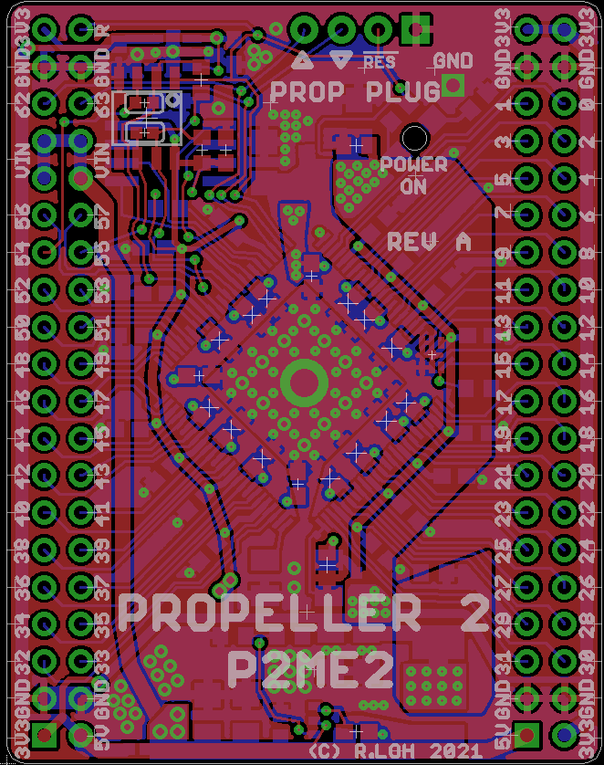
@jmg, I increased a ground plane on most of the left header pin pads. There's still a thinner strip of ground remaining between VCCIO and VIN trace, am wondering if it is better to take VCCIO bypass cap grounds off that or not. I have a mix now.
@rogloh said:
@jmg, I increased a ground plane on most of the left header pin pads.
That’s looking good, but by stitching vias, I was meaning vias in pairs to jumper/ straddle that vin trace. That makes the overall gnd appear more complete.
ie add a via above the 7 of 37 and above the 1 of 41 and so forth.
I also wondered about ferrite bead pad options on the 3v3 legs to P2 ?
Addit: there may be room for a similar via stitch between 17 & 15 texts on rhs?
Ok I added vias on 37 and 41 but no more. I will be sending this version out to Lachlan. If it's no good with too much noise on VCCIO affecting things then I'll do more changes on another revision.
I only want to get this done so I don't need to respin this complex beast, which is already partially soldered. It was showing signs of life a couple of years ago before being put on hold waiting for P2D2:
P2ME2 boards arrived today and I'm quite happy with the result so far, the silkscreen is nice and legible too. Apologies for the low quality images, I have rather poor lighting here at night with these overhead close up shots and the very reflective tinned surface doesn't help either.
Still waiting on the stencil and maybe a couple of extra parts before assembly can begin.
Thanks @Publison , yeah I know, fingers crossed. That little 1.8V regulator (U2) is going to be the challenge. Thankfully many of its pins are shared with neighboring pins so even if there is a bridge under it in some places, it could still work. Maybe hot air reflow with flux and paste applied under it could work even without the stencil but I've only got a couple of these parts to play with at this point. If that hot air worked I think I could probably hand solder the rest ok, including the P2 with care.
@JRoark , Cheers, it was PCBWay. Have been quite satisfied with their proto quality in the last several boards they've made for me. That deal they have for $5 to get 10 2-layer boards made up to 10x10cm in size is pretty awesome.
@rogloh said:
Thanks @Publison , yeah I know, fingers crossed. That little 1.8V regulator (U2) is going to be the challenge. Thankfully many of its pins are shared with neighboring pins so even if there is a bridge under it in some places, it could still work. Maybe hot air reflow with flux and paste applied under it could work even without the stencil but I've only got a couple of these parts to play with at this point. If that hot air worked I think I could probably hand solder the rest ok, including the P2 with care.
Nice looking board
For a single critical part, or even that plus the P2, you could try hot plate reflow ?
I finally received my electronic hotplate for surface mounting components and gave it a try for the first time, with just a subset of my P2ME2 board components. Inspected soldering results mostly looked satisfactory initially but I don't measure 1.8V on the regulator output when I feed it with 3.3V, I see only values from 0.3V...1V - (this might be due to being unloaded?, still testing that) - EDIT, added 47ohm load to 1.8V, now get zero output on 1.8V output cap, did I fry it? . Also I only had some refrigerated solder paste on hand that was somewhat beyond its use by date which is hardly good either, I will definitely need to order some more. Regardless of that it seemed to flow nicely and evenly onto the board when I squeegeed it on through the stencil, and it made good connections to the other components when I measured them but it is hard to know how good the tiny 1.8V SMD regulator connection was underneath that part. I don't think there are shorts at least. I know I placed it very carefully without smudging it and it was well centered too and pin 1 was oriented correctly (despite its microscopic marking).
Another problem I found was measuring the PCB temp properly as I couldn't yet make a solid connection to my thermocouple while reflowing and resorted to holding it by hand. So lots of room for errors here really. Maybe I could try to reflow it again if required to see if that helps.
If I can get this tiny SMD regulator going, I'm confident I can solder the remaining components by hand, including the 0.5mm P2 which will be fun (not). I think I'd have enough parts for at least two more attempts before I will need to order some more components.
The 2nd reheat reflow attempt didn't fix this board unfortunately. Pretty sure I got it into the right temp range too. So maybe the EN or FB pin of the regulator is not soldered properly under the part, or I overcooked it somehow? Need another attempt with a better temperature probing setup. Will need to buy some kapton tape to stick it down plus some fresh solder paste to be more confident there too I guess. Another wait...this lockdown sucks, I can't just drive down to my local Altronics or Jaycar for this simple stuff.
@rogloh said:
The 2nd reheat reflow attempt didn't fix this board unfortunately. Pretty sure I got it into the right temp range too. So maybe the EN or FB pin of the regulator is not soldered properly under the part, or I overcooked it somehow?
You could remove it with a hot-air iron, and try again ?
Yeah possibly, but I don't have any hot air rework gear here at this time either and so I would need to order that too. Or I could just use another board, as I had 10 made. I can always try to salvage the other active parts too if urgently needed once I run out of these devices. That SOP-8 flash is not too hard to remove with a regular iron and desolder braid.
U2 middle left pin (2?) doesn’t look like a lot of solder.
Sounds like your paste is fine. Mine expired over 5 years ago but it has been kept refrigerated and sealed. It’s a little dry so I now mix a tiny bit of isopropyl alcohol with a little paste and never return anything back to the original jar. I have a second jar to decant and/or dispose. Never had a problem - reflows nicely every time but my oven is nicely profiled.
After you have applied the paste does it look nicely formed? ie not slumping but nice edges? If it’s too dry it will partially lift back in the screen, if too wet it will tend to slump ie slightly run. It’s hard to describe. So the lands on the P2 pins should be nicely registered and not running into each other.
Yes @Cluso99 , despite being out of date the paste actually seemed quite good to me (I had left it out overnight and unopened to warm up too). Solid enough edges formed on the pads but they still remained moist as well. There's not a lot of paste applied for the pads on U2 as they are quite small, but each pad certainly had some paste on it and it was well registered, and after the reflow had the U2 part sunk down so all connections should have been made IMO.
The thing is about this regulator module is that adjacent pads are often shared with neighbouring pads (ie. multiple VIN, VOUT, GND pins) so if one of those multiple connections was not completed and a least one its neighbours was then it should still be able to operate (at lower load current). I don't think anything would have shorted as there wasn't a large amount of paste under there so I'm still at a loss as to what happened. Maybe the caps were no good... or I had a bad part or I overcooked it? If anything I thought I undercooked it the first time and got the reheat temp right the second time. I do see what looks like a couple of tiny solder balls sticking out the bottom edge of U2 so maybe it didn't fully melt there? Can't quite tell. Also C24 bottom edge didn't look clean in this image but it was electrically connected, in any case I touched it up with the iron manually later but it didn't help.
Update: Another thing I'll have to add to my growing laundry list of updated tools is to get some better inspection gear. Could help identify any solder faults a bit easier.
@Tubular said:
Are you sure its not the adjustable version of that regulator?
No, the part I ordered and was labelled as such on the packet, is this one:
TPSM828222SILR
It should be 1.8V fixed output (@2A max).
The 0.3~1v thing is interesting, i'm wondering whether that indicates an issue with the feedback pin
Yeah I thought the same when I measured it, but soon after I added a small 47 ohm load I noticed it dropped to zero voltage and hasn't driven out anything since which is also weird. No input current from the supply seems to be getting drawn (on the supply's ammeter with 10mA resolution) but I should measure with another meter using a smaller current scale to see if any current is flowing at all, though its quiescent is less than 10uA and shutdown current is below 0.5uA so it would be hard to see much there anyway. If the EN pin is floating maybe it could be stuck in shutdown perhaps, but the PG output I have hooked to P2's RESET is floating, indicating it's either not connected into the regulator's pin, or VIN < 0.7V. Earlier I had seen this PG pin pull low too, but it is now not doing that.
If the enable pin (EN - pin 3) is left floating (unconnected) , or it got shorted to power good (PG - pin4), the resulting effect will be exactly the one you're describing.
Did you used a continuity meter, in order to check for any non-obvious open/short circuits in that region?
@Yanomani said:
If the enable pin (EN - pin 3) is left floating (unconnected) , or it got shorted to power good (PG - pin4), the resulting effect will be exactly the one you're describing.
Did you used a continuity meter, in order to check for any non-obvious open/short circuits in that region?
The EN pin 3 is bonded via copper to VIN pins 1,2 under the device, the bottom layer footprint in reverse is shown below.
Pin 4 is PG and snakes through underneath the part to the P2 reset - I'd guessed it could have shorted but I only measured the 47k reset pullup resistor resistance between 3.3V and this PG output so it shouldn't be shorted to ground or VIN. Other pads are GND, VIN, VOUT and there are no shorts between those signals. Maybe EN pad 3 is floating with a bad connection or the part is bad/went bad...
EDIT: Actually I do measure 38 ohms from PG out to GND, but this is probably expected when the device is unpowered, it's not a dead short.
If you don't already own one, remember to order a micro/mini vacuum suction pen tool along with the hot air stuff.
You will really enjoy being able to "pull-off that smt dwarf" as fast as possible (without peeling-off the land patern), before there is too much time for any yet unsoldered pin(s) to re-reflow, so you can get a real feeling about it/they got evenly seated/weated before.
Bad smt solder joints uses to leave footprints, as dogs do, like "muddy" spots on the floor.
EDIT: Actually I do measure 38 ohms from PG out to GND, but this is probably expected when the device is unpowered, it's not a dead short.
Fifty (even fourty) years ago, and I would be sure something was really weird about these 38 Ohms; when unbiased, simple open-collector (even N-Mos open-drain) outputs would never measure anything this low, but, who knows what that "huge amount" of artisans, working like bees, for those city-wide fabs, are stuffing into those standard cells?
There was a time (not too long ago), when TI used to do a fine detailing, about almost everything it layed onto silicon. Now, everyone is expected to be lucky, by getting those darning "block diagrams". Too sad...
Even strawberry waffles packages get better detailled about its contents, at any supermarket shelves...
In order to don't copy any detail of a third-part product directly, please take a look at TI's datasheet, page 8, topic "8.2 Functional Block Diagram":
I really doubt that low-value is ever possible (while unbiased)...
P.S. In case there are some spare parts laying arround, perhaps you can measure that value, and cross-compare the results.
P.S. II - Since there are not any "too sensitive" circuits mounted on the pcb, and in order to avoid innadvertently biasing the gate-driver with the VOM, please try reversing the probes, to be sure it's really a plain resistor-alike path.


Comments
I think it is very important to place the bypass caps as close as possible to the P2. Even a short trace of only 1/2 or 1/4 inch makes a inductance of a few nH which forms a series resonant tank together with the cap and renders it useless for high frequencies. C26, C27 and some others are too far away, in my opinion.
Hi rogloh
I know that can be too late for a warning, and also no one know that pcb better than you, but would you mind putting some references for JP1/JP2, at least at the silk screen masks, perhaps near their "Pin 1" designations.
Since you've provided the Prop Plug "Pin 1" with a nice square pad identifier, perhaps it would also be good to have the same ID at JP1 and JP2, but this would demmand more that a little editing to settle.
Sorry for the late comment, but I was out almost the whole morning, so only saw your last designs just about now.
Henrique
Yes, I found it's a bit of challenge to get the VCCIO bypass caps all close without chopping off the wide ground current path for good heat spread on a two layer board. A two layer board is going to be a bit of a compromise there. I'll continue on a rev B version today to try to squeeze them a little closer and see if there is a little more time today to try to get that version used.
No worries. Looks like I had missed that lack of a square pad in the part I placed. Normally the pin 1 pad is square on headers but is not in this part I grabbed from some random library. Yeah I should try to identify it. There are JP1 and JP2 labels down on the bottom layer but pin 1 is not properly identified.
While I'm at it I probably should add P2 pin number labels down the side. But I really don't want this to turn into a full blown P2D2. My P2ME2 is a poor man's P2D2. The "Clayton's" P2D2 if you like.

https://en.wiktionary.org/wiki/Claytons
I didn't found them at the last transparent view you've uploaded, but now that you said they are there, I see it's a matter of which layers are active when a particular view is generated.
Was able to check the labels at a previous post (2021-06-23 22:38 (refered to my own GMT-3 time zone)), but will avoid linking it at this post, so as to don't confuse noone.
Pin 1 id's are welcome. Trice more, as eyesight worsens... :sad:
As for the "Clayton's" drink, I suggest you to take a look at the following brazilian recipe:
https://braziliankitchenabroad.com/quentao-brazilian-grog-cocktail/
"Quentão" is a very popular "winter's drink" many people uses to take a lot, when she/he isn't going to assume that even wanna drink, at all!
Pity it has a lot of sugar, so I don't have it, due MD restrictions. :sad: :sad:
I added pin labels, pin 1 identifiers and tried to bring in some bypass caps a bit closer, more work could be done there for the bypass caps near the flash pins but it would need longer. That area needs more work, but I think this will do for now.
Sneaking a gnd finger into the 3v3 split plane is a good idea, but there could be more copper for that, stolen from the inductor cooling finger ?
There may be room on the left to sneak in some stitching vias, so the poured gnd area under connector can become a useful plane ? On rhs that works well.
Yeah, I stole a bit from the inductor cooling and could take a bit more, would quite like to do the same on the top right but don't trust the heat output from 1.8V regulator - it's an unknown and I want to cool as much as I can so I left it in place. Two layers is tough (at least for me).
Yes I will take a look at that. I don't want to pinch off the path through from the VCCIO bypass cap grounds at upper left which might take a convoluted path. It could be a VIN plane, but having that 12V go right past all port B P2 signals is probably not ideal. Using it as a ground would be safer.
@jmg, I increased a ground plane on most of the left header pin pads. There's still a thinner strip of ground remaining between VCCIO and VIN trace, am wondering if it is better to take VCCIO bypass cap grounds off that or not. I have a mix now.
That’s looking good, but by stitching vias, I was meaning vias in pairs to jumper/ straddle that vin trace. That makes the overall gnd appear more complete.
ie add a via above the 7 of 37 and above the 1 of 41 and so forth.
I also wondered about ferrite bead pad options on the 3v3 legs to P2 ?
Addit: there may be room for a similar via stitch between 17 & 15 texts on rhs?
Ok I added vias on 37 and 41 but no more. I will be sending this version out to Lachlan. If it's no good with too much noise on VCCIO affecting things then I'll do more changes on another revision.
I only want to get this done so I don't need to respin this complex beast, which is already partially soldered. It was showing signs of life a couple of years ago before being put on hold waiting for P2D2:
By the way what happened to the P2D2 and @"Peter Jakacki" ?
Mike
P2ME2 boards arrived today and I'm quite happy with the result so far, the silkscreen is nice and legible too. Apologies for the low quality images, I have rather poor lighting here at night with these overhead close up shots and the very reflective tinned surface doesn't help either.
Still waiting on the stencil and maybe a couple of extra parts before assembly can begin.
Looks great. Fingers crossed for good reflow.
Roger: which PCB vendor did you use for this? Looks great btw!
Thanks @Publison , yeah I know, fingers crossed. That little 1.8V regulator (U2) is going to be the challenge. Thankfully many of its pins are shared with neighboring pins so even if there is a bridge under it in some places, it could still work. Maybe hot air reflow with flux and paste applied under it could work even without the stencil but I've only got a couple of these parts to play with at this point. If that hot air worked I think I could probably hand solder the rest ok, including the P2 with care.
@JRoark , Cheers, it was PCBWay. Have been quite satisfied with their proto quality in the last several boards they've made for me. That deal they have for $5 to get 10 2-layer boards made up to 10x10cm in size is pretty awesome.
Nice looking board")
For a single critical part, or even that plus the P2, you could try hot plate reflow ?
Thanks to you (and others) in helping me to try to improve it. Let's hope it actually works...
Or even with a clothes iron, like this...lol
I finally received my electronic hotplate for surface mounting components and gave it a try for the first time, with just a subset of my P2ME2 board components. Inspected soldering results mostly looked satisfactory initially but I don't measure 1.8V on the regulator output when I feed it with 3.3V, I see only values from 0.3V...1V - (this might be due to being unloaded?, still testing that) - EDIT, added 47ohm load to 1.8V, now get zero output on 1.8V output cap, did I fry it? . Also I only had some refrigerated solder paste on hand that was somewhat beyond its use by date which is hardly good either, I will definitely need to order some more. Regardless of that it seemed to flow nicely and evenly onto the board when I squeegeed it on through the stencil, and it made good connections to the other components when I measured them but it is hard to know how good the tiny 1.8V SMD regulator connection was underneath that part. I don't think there are shorts at least. I know I placed it very carefully without smudging it and it was well centered too and pin 1 was oriented correctly (despite its microscopic marking).
Another problem I found was measuring the PCB temp properly as I couldn't yet make a solid connection to my thermocouple while reflowing and resorted to holding it by hand. So lots of room for errors here really. Maybe I could try to reflow it again if required to see if that helps.
If I can get this tiny SMD regulator going, I'm confident I can solder the remaining components by hand, including the 0.5mm P2 which will be fun (not). I think I'd have enough parts for at least two more attempts before I will need to order some more components.
Some pics of the first PCB attempt.
The 2nd reheat reflow attempt didn't fix this board unfortunately. Pretty sure I got it into the right temp range too. So maybe the EN or FB pin of the regulator is not soldered properly under the part, or I overcooked it somehow? Need another attempt with a better temperature probing setup. Will need to buy some kapton tape to stick it down plus some fresh solder paste to be more confident there too I guess. Another wait...this lockdown sucks, I can't just drive down to my local Altronics or Jaycar for this simple stuff.
You could remove it with a hot-air iron, and try again ?
Yeah possibly, but I don't have any hot air rework gear here at this time either and so I would need to order that too. Or I could just use another board, as I had 10 made. I can always try to salvage the other active parts too if urgently needed once I run out of these devices. That SOP-8 flash is not too hard to remove with a regular iron and desolder braid.
U2 middle left pin (2?) doesn’t look like a lot of solder.
Sounds like your paste is fine. Mine expired over 5 years ago but it has been kept refrigerated and sealed. It’s a little dry so I now mix a tiny bit of isopropyl alcohol with a little paste and never return anything back to the original jar. I have a second jar to decant and/or dispose. Never had a problem - reflows nicely every time but my oven is nicely profiled.
After you have applied the paste does it look nicely formed? ie not slumping but nice edges? If it’s too dry it will partially lift back in the screen, if too wet it will tend to slump ie slightly run. It’s hard to describe. So the lands on the P2 pins should be nicely registered and not running into each other.
Yes @Cluso99 , despite being out of date the paste actually seemed quite good to me (I had left it out overnight and unopened to warm up too). Solid enough edges formed on the pads but they still remained moist as well. There's not a lot of paste applied for the pads on U2 as they are quite small, but each pad certainly had some paste on it and it was well registered, and after the reflow had the U2 part sunk down so all connections should have been made IMO.
The thing is about this regulator module is that adjacent pads are often shared with neighbouring pads (ie. multiple VIN, VOUT, GND pins) so if one of those multiple connections was not completed and a least one its neighbours was then it should still be able to operate (at lower load current). I don't think anything would have shorted as there wasn't a large amount of paste under there so I'm still at a loss as to what happened. Maybe the caps were no good... or I had a bad part or I overcooked it? If anything I thought I undercooked it the first time and got the reheat temp right the second time. I do see what looks like a couple of tiny solder balls sticking out the bottom edge of U2 so maybe it didn't fully melt there? Can't quite tell. Also C24 bottom edge didn't look clean in this image but it was electrically connected, in any case I touched it up with the iron manually later but it didn't help.
Update: Another thing I'll have to add to my growing laundry list of updated tools is to get some better inspection gear. Could help identify any solder faults a bit easier.
Are you sure its not the adjustable version of that regulator?
The 0.3~1v thing is interesting, i'm wondering whether that indicates an issue with the feedback pin
No, the part I ordered and was labelled as such on the packet, is this one:
TPSM828222SILR
It should be 1.8V fixed output (@2A max).
Yeah I thought the same when I measured it, but soon after I added a small 47 ohm load I noticed it dropped to zero voltage and hasn't driven out anything since which is also weird. No input current from the supply seems to be getting drawn (on the supply's ammeter with 10mA resolution) but I should measure with another meter using a smaller current scale to see if any current is flowing at all, though its quiescent is less than 10uA and shutdown current is below 0.5uA so it would be hard to see much there anyway. If the EN pin is floating maybe it could be stuck in shutdown perhaps, but the PG output I have hooked to P2's RESET is floating, indicating it's either not connected into the regulator's pin, or VIN < 0.7V. Earlier I had seen this PG pin pull low too, but it is now not doing that.
If the enable pin (EN - pin 3) is left floating (unconnected) , or it got shorted to power good (PG - pin4), the resulting effect will be exactly the one you're describing.
Did you used a continuity meter, in order to check for any non-obvious open/short circuits in that region?
The EN pin 3 is bonded via copper to VIN pins 1,2 under the device, the bottom layer footprint in reverse is shown below.
Pin 4 is PG and snakes through underneath the part to the P2 reset - I'd guessed it could have shorted but I only measured the 47k reset pullup resistor resistance between 3.3V and this PG output so it shouldn't be shorted to ground or VIN. Other pads are GND, VIN, VOUT and there are no shorts between those signals. Maybe EN pad 3 is floating with a bad connection or the part is bad/went bad...
EDIT: Actually I do measure 38 ohms from PG out to GND, but this is probably expected when the device is unpowered, it's not a dead short.
Thanks for taking the time to test it.
If you don't already own one, remember to order a micro/mini vacuum suction pen tool along with the hot air stuff.
You will really enjoy being able to "pull-off that smt dwarf" as fast as possible (without peeling-off the land patern), before there is too much time for any yet unsoldered pin(s) to re-reflow, so you can get a real feeling about it/they got evenly seated/weated before.
Bad smt solder joints uses to leave footprints, as dogs do, like "muddy" spots on the floor.
Fifty (even fourty) years ago, and I would be sure something was really weird about these 38 Ohms; when unbiased, simple open-collector (even N-Mos open-drain) outputs would never measure anything this low, but, who knows what that "huge amount" of artisans, working like bees, for those city-wide fabs, are stuffing into those standard cells?
There was a time (not too long ago), when TI used to do a fine detailing, about almost everything it layed onto silicon. Now, everyone is expected to be lucky, by getting those darning "block diagrams". Too sad...
Even strawberry waffles packages get better detailled about its contents, at any supermarket shelves...
In order to don't copy any detail of a third-part product directly, please take a look at TI's datasheet, page 8, topic "8.2 Functional Block Diagram":
I really doubt that low-value is ever possible (while unbiased)...
https://ti.com/lit/ds/symlink/tpsm82822.pdf?ts=1630231169669&ref_url=https%253A%252F%252Fwww.ti.com%252Fproduct%252FTPSM82822
P.S. In case there are some spare parts laying arround, perhaps you can measure that value, and cross-compare the results.
P.S. II - Since there are not any "too sensitive" circuits mounted on the pcb, and in order to avoid innadvertently biasing the gate-driver with the VOM, please try reversing the probes, to be sure it's really a plain resistor-alike path.