@SaucySoliton said:
At 85MHz you may need individual ground wires like those old 80 conductor IDE cables. Or a dedicated PCB
Exactly.
The PCI bus has 20 ground pins for 32+ data pins and that's only 33 MHz. That 40 pin FPC connector only has 3? ground pins for 24+ data pins. And ground lines need to run closely parallel to the data lines.
Yep. In fact in this broken test setup with the split ribbon cable I only have one ground wire going to the P24-P31 header. All the others pixel groups don't even have a ground wire which I know is bad, it's the first start. I was also surprised when I discovered the Adafruit board only brings out 3 grounds onto the flat flex connector and that's got to be shared with power and backlight current. Unless I make my own TPF401 board I can't do much about that aspect, but I can eliminate the 40 way 0.05 inch header ribbon and surround signals with grounding on a real PCB. I think this should help somewhat and it'd be easy to spin a quick connector board for P2-EVAL.
You could enable registered input on only some pins.
I could attempt that - with a proper test pattern it might be good to try this. I realized I should be using my Mac laptop HDMI to drive this instead of the RasPi. I can then set up mirroring mode and actually see what I'm sending rather than being blind during capture so to speak. I can also code some test pattern graphics using this approach too.
Chris Gadd posted a USB mass storage device program here https://forums.parallax.com/discussion/comment/1561434/#Comment_1561434 I didn't have any luck yet with the included SD card driver, but it was easy to use hub ram instead as a 128kB disk. I think it would be easy set it up to use the PSRAM. Just remember that the USB device board dm pins are 18 and 20, not 16 as set in the zipfile. I've been working on a USB video class device which I should be posting soon.
That seems very interesting and cool, will definitely have to take a look at what Chris did, and a USB video class sounds very handy as well. You're often working on interesting things Saucy. There's still a lot of fertile ground for USB and P2.
Chris Gadd posted a USB mass storage device program here https://forums.parallax.com/discussion/comment/1561434/#Comment_1561434 I didn't have any luck yet with the included SD card driver, but it was easy to use hub ram instead as a 128kB disk. I think it would be easy set it up to use the PSRAM. Just remember that the USB device board dm pins are 18 and 20, not 16 as set in the zipfile. I've been working on a USB video class device which I should be posting soon.
That seems very interesting and cool, will definitely have to take a look at what Chris did, and a USB video class sounds very handy as well. You're often working on interesting thing Saucy. There's still a lot of fertile ground for USB and P2.
I second that.
Also, super interested in the USB video class. Have had success with the tinyusb UVC example on RP2040 (driven by data from the P2), but would love to get it all inside the P2
I looked at the pixel data. Those bright pixels at the top of the 'grey folder icon' correspond to where the gradient steps from grey 127/127/127 to (white 255/255/255 or yellow pixel) to grey 129/129/129. So its not coping with so many data lines changing state all at once, or so it seems.
Shorter wires? tin foil? buffer ICs? terminations? lvds? But great to see it doing as well as it is
Here is the USB video class code. It was a bit more work than just changing the configuration descriptor. UVC devices need to respond to PROBE and COMMIT requests for the format. It turns out that at least on Linux, UVC devices are suspended when not in use. To cleanly exit suspend the device needs to respond to the GET_STATUS request.
It can only use about 25% of the available bandwidth right now. Turns out we get one isochronous packet per frame. Since a frame is 1 mS, to get 1MB/sec the isochronous packet needs to be 1000 bytes. Up to 1023 bytes is allowed. But the code uses a byte to store the packet length. So for now it sends 252 bytes of payload per packet. Bulk transport is an option.
Thanks @ChrisGadd for posting USB device code which is much cleaner than the one I made from the USB host code.
@Tubular said:
I looked at the pixel data. Those bright pixels at the top of the 'grey folder icon' correspond to where the gradient steps from grey 127/127/127 to (white 255/255/255 or yellow pixel) to grey 129/129/129. So its not coping with so many data lines changing state all at once, or so it seems.
Shorter wires? tin foil? buffer ICs? terminations? lvds? But great to see it doing as well as it is
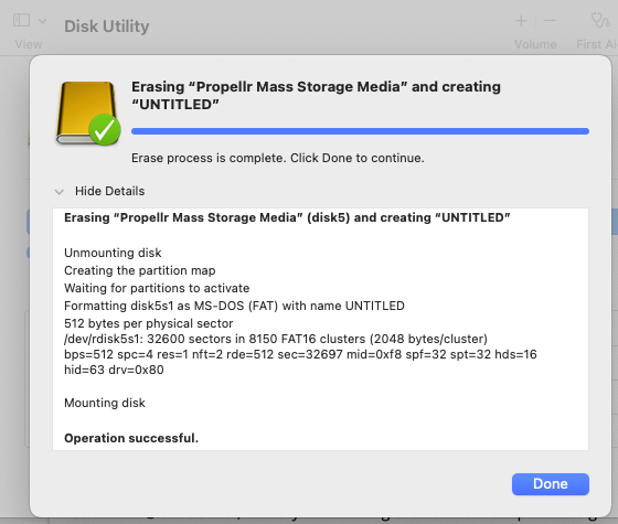
Yeah that's a good data point you found @Tubular and there's a lot of IO pins switching current at this time so I think better grounding will help and I want to try your suggestions. Am currently working through Chris Gadd's very nice USB client code and have had some initial success reading/writing a USB mass storage from PSRAM (right now my Mac wants to format with FAT16 given the size of PSRAM is only supporting a 32MB volume). I also want to get onto designing a quick interface PCB for P2-EVAL.
For this PCB I will put the 40 pin FPC connector to attach to the TFP401 board and pads for 32MB of SOP PSRAM using P40-P57 (same as P2-EDGE mapping), and put a pogo pin pad for pass through of a (jumpered) clock to the XI pad directly below and either leave a cut out for using P32-P39 with existing breakout boards for HDMI/VGA/4 bit SD use - or possibly bring that accessory header up to the top surface for plugging in there. Also I'll add this USB client interface somewhere into P24-P31 which hopefully won't interfere with P2-EVAL PLL too much if it runs at only 12Mbps...somewhat TBD there. I might be able to shuffle control bits around a little and put the lower frequency signals onto the upper nibble like the Vsync and Active signals, and keeping CLK, DE, HSYNC and USB D+/D- further down in the 8 bit group. The pixel clock should be jumper-able through to the IO pin or to the XI for both sync/async applications. I can probably throw a small STEMMA JST-SH connector in parallel with that USB client port to help program the Adafruit board EDID from the P2 if needed. Also some mounting holes for the Adafruit TFP401 board and to sit above allowing shorter FFC cabling would be the icing on the top.
@SaucySoliton said:
Here is the USB video class code. It was a bit more work than just changing the configuration descriptor. UVC devices need to respond to PROBE and COMMIT requests for the format. It turns out that at least on Linux, UVC devices are suspended when not in use. To cleanly exit suspend the device needs to respond to the GET_STATUS request.
Cool, thanks for posting. Will take a look when I can.
It can only use about 25% of the available bandwidth right now. Turns out we get one isochronous packet per frame. Since a frame is 1 mS, to get 1MB/sec the isochronous packet needs to be 1000 bytes. Up to 1023 bytes is allowed. But the code uses a byte to store the packet length. So for now it sends 252 bytes of payload per packet. Bulk transport is an option.
Thanks @ChrisGadd for posting USB device code which is much cleaner than the one I made from the USB host code.
Yes thanks @ChrisGadd , it's very nice looking code and should provide a great framework/template for a variety of USB devices. Straightforward endpoint interfaces simplify things a lot. I've dug through the host side USB code which is complex (has to be) and this is so much easier to follow.
Many thanks for posting that UVC code James, and thanks to Chris for the tidy device code
Unfortunately we didn't have any luck with the 4 windows 10/11 machines we tried it on. The PCs initially make promising 'connected' system beeps, but the P2 doesn't show up as a webcam. Device manager says the device status is as follows: "This device cannot start. (Code 10)"
I think you're using Linux, we might get a ubuntu box up and running and try it there. Or we can give you remove Anydesk access to the windows machine with P2 hardware attached, if that would help
We did have some similar issues with Kye's OpenMV doing its UVC using STM32 processors - there were some quirks with windows that the developers didn't see on their linux systems. These might have been resolved by now though.
Hi @SaucySoliton . I tried out your UVC code today.
On my Mac Mini running Ventura macOS it reports a camera present name as VID7504:PID24880 in the PhotoBooth webcam application supplied with the system but the video screen output just remains black. The P2 appears to be hung waiting in this loop and never exits. I suspect the endpoint is not allowed to be sent to by the Mac, maybe due to some type of validation failure (possibly unhappy with the PID/VID).
On my Ubuntu 24.04 Linux running on my older x86 MacBookPro I see USB UVC attachment logs in dmesg output etc but the Camera application hangs when trying to record anything and the screen remains black if left in a preview state. So no luck there either unfortunately. It does let the loop above execute though vs the macOS setup so it does get a bit further.
Hi @VonSzarvas , I'm going to be laying out my P2-EVAL interface board soon for the FFC interface to the TFP401 board and wonder if I can request from you the X,Y relative distances between let's say the P2's IO pin P32 located at the IDC header pin co-ordinate (hole centre) and the XI pin pad hole on the RevB P2-EVAL 1928 datecoded PCB. That'd help me locate the pogo pin directly above it for optional feeding in the pixel clock to the P2 X-input in synchronous applications. Not sure if that XI pad co-ordinate changed on later P2-EVAL rev PCBs. If it has I might be able to put in drill holes at alternate positions on my board as well if your have those dimensions also.
Do you have a Gerber viewer? The attached will give you every gory detail, and might be handy to import to your layout software as a template for your own interface board?
Otherwise I measured a few things in the images (all dims in millimeters)... maybe too much information :-)
Thanks @VonSzarvas . It's very much appreciated. Certainly more than I needed for this one but it will be useful for any future board developments or by anyone else making boards to sit directly above the P2-EVAL. Definitively nicer than just trying to eyeball it with ruler or try to caliper everything. You can get close doing that but it's not always perfect.
Yes I do have a Gerber viewer (Gerbv) somewhere.
One more question, does the RevC P2-EVAL keep the XI pad in the exact same location? The picture of it online seems to show that it didn't change position but I can't tell for sure.
I've started working on my interface board today and routed some of the 32MB PSRAM using that inner PSRAM memory board I made previously as a reference. Will just add the FPC connector and and a micro-USB socket for USB client transfer and it'll be close to done. Was thinking of vampire tapping off power from the P2-EVAL to supply the Adafruit board but the TFP401 datasheet mentions it draws about 370mA at 82.5MHz so it's a bit of a hog for current and probably deserves it's own power. However I might still route it and enable a path via some header pins for convenience. Will see...
I do wish there were a few more IO pins left over for a 4 bit SD card interface to be added onto this board too, but that can always be fitted to P32-P39 if it will be used in a capture only setup. Otherwise placing an output port there makes sense (HDMI or VGA/AV). Bringing out 3 pin component video is another option as it doesn't need a lot of pins...hmmm. Would love to put YCrCb on P29-P31 but it could kill the PLL supply integrity that is sharing the upper nibble of port A. I wonder if the video DAC output behaves nicer than noisy high speed data transitions. Be worth a try I guess. Maybe that won't affect the PLL so much.
does the RevC P2-EVAL keep the XI pad in the exact same location?
Yes.
Was thinking of vampire tapping off power from the P2-EVAL to supply the Adafruit board but the TFP401 datasheet mentions it draws about 370mA at 82.5MHz so it's a bit of a hog for current and probably deserves it's own power.
If 5V, then can't imagine that would be an issue. If 3.3V, then you'll be fine if the Vxxxx port you use isn't doing much else. AFAIR, those 3.3V regulators are rated for 500mA, and easily supply 600mA constant current. The peak pulse will be somewhere above that, not mega, but probably a good 100mA from memory, so at higher frequency they should have the oomph you need. I'd suggest it's worth the time to try.
Or else use the AUX usb support port, and tap 5V from the 2-pin header about that USB port, direct into your accessory board?
Made a bit more progress on this HDMI capture interface board, which is now something I'm now calling the "Blue Ringed Octopus" (look it up).
Still have to work the header pin interface labels and maybe add a Stemma/Qwiic style I2C port where that dummy micro-USB socket placeholder is located although it could be handy to leave that type of connector somewhere else on the board as it would only need to be passively connected through series resistors and wouldn't interfere with other boards if left unplugged. I found I could route the top 4 free port A IO pins (P28-P31) to a breakout header adjacent to the P2 header connector. This would at least allow one USB port from either the Parallax USB client board or USB host board to operated if plugged in there. I also routed the pixel clock pin to pin "24" of this adjacent port yielding 5 IO pins total which may allow YUV/RGsB video+LR audio in the "sync" mode when the pixel clock is not routed to an IO pin but to XIN instead (although I tried outputting VGA on P28-P31 and found it did cause PLL jitter problems with VGA at 325MHz just now in a quick test, might be okay with other applications/drive strengths etc or with the sync input clock going into XIN, don't know yet). Probably shouldn't harm anything to bring the clock to that header pin if the clock for async mode operation will max out at around 27MHz anyway.
I could possibly route through P22-P24 P25-P27 as well so this octopus board could be used as a basic PSRAM board and still get more access to the otherwise covered IO pins while P32-P39 on the P2-EVAL is kept completely open to plug in any Parallax single wide breakout board. I was wondering about bringing out more of the P58-P63 signals but didn't have a particular idea in mind, plus these pins are harder to re-use on P2-EVAL anyway. It'd be really neat if we could put a micro-USB connector path on P62-P63 for standalone high speed USB serial client access (around 1MB/s) but the FTDI chip RX signal will likely interfere with it, so we would need to resort to other pins for that.
Hoping the clock path will be okay for high speed signals up to 85MHz or so. The XIN pad is directly above and suits a pin header or pogo style header. Drill size is 0.7mm for pogo but could be enlarged after manufacture for square pin header pass through. The bottom layer is mostly ground plane. Just has a few cuts for power tracks and for PSRAM at the periphery. Most of the high speed signals have a nice ground below them and I'm making use of all the ground pins plus the power ground from the TFP401 board as well. This should help remedy the potential ground bounce effects I might have been encountering with the simple split IDE cable approach I used in my prototype setup.
I want to keep this interface board simple and wrap it up quickly but were there any other thoughts from others while I'm still at it? I could add a power LED given this covers most of the P2-EVAL, maybe a P2 reset if the HDMI capture output is not active (this could be useful in sync applications when the pixel clock is not recoverable).
Current pin mapping is this:
P0-P7 - RED
P8-P15 - GREEN
P16-P23 - BLUE
P24 - CLOCK (async)
P25 - DE
P26 - VSYNC
P27 - HSYNC
P28-P39 - FREE
P40-P55 - 16 bit PSRAM DATA
P56 - PSRAM CLK
P57 - PSRAM CE
P58-P63 - P2 FLASH/SD/FTDI
Colour byte lanes are not aligned with P2's preferred RR_GG_BB_XX byte order for output, but best suits the HW signals from the FPC connector. A single MOVBYTS fixes the order. Flipping the TFP401 board around could also fix that, but I don't want to risk feeding high speed colour bits into P28-P31.
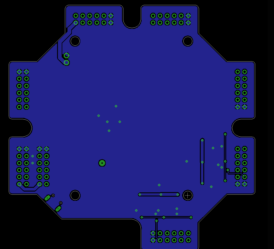
Getting closer...mainly now need to check clearances, label names/sizes, final positions, etc.
I've added a Qwiic SMD (JST-SH) 4 pin connector on P28,P29 with a 5V VCC power path, and a micro-USB client port for P30, P31. These are non-conducting signal paths when left disconnected and won't affect operation of breakouts plugged into the P24-P31 header. The I2C port is useful for re-programming the 5V Adafruit EDID, just needs a Qwiic/Stemma QT cable. The USB client will (hopefully) be useful for a fast upload of grabbed frames to a host or for other purposes. I also look at P62,P63 for potential USB client port and in theory you could re-use these for USB if the FTDI USB port is left disconnected/idle given the 10k series resistor coupling but it's far better used for download/debug testing as it is. As yet I haven't added the reset path from this board to the P2. If put in it would need to be made optional via a solder jumper. Also added were diamond pattern mounting holes that line up with the P2-EVAL holes below in case the boards are fixed together more firmly in a stack - LOL, as if the IDC headers won't hold it tightly enough already! A short 5cm folded flat flex cable should wrap around under the Adafruit board to the mating FPC40 ZIF connector which has been lined up for that. Gotta check the folded length reaches too.
Roger, I don't know your application for this board but if I was designing it I would be tempted to shuffle data lines around to support 16 bit color capture. Not sure if that would affect the timing.
Because the streamer selects only to 8 pin boundaries, the pins need to be offset a bit so the +/- 3 input window can straddle the desired pins. I think native left-justified RGB32 can be captured by letting it wrap around from pin 56 to pin 0-23. Except then you loose pins 0-1. The color space converter should be able to fix the R/B swap.
@SaucySoliton said:
Here is the USB video class code.
@SaucySoliton This makes the P2 act like a USB camera, is that right?
Looks like set for image size of 128x96 at 30Hz in YUY2 format?
Yes. x2 It works well for me on Linux, but Windows and Mac have issues. It doesn't give 30 fps yet, maybe 10. It's a bandwidth limitation. The fix is to move to bulk streaming, or rewrite enough to support isochronous packets up to 1023 bytes.
@rogloh said:
Getting closer...mainly now need to check clearances, label names/sizes, final positions, etc.
I've added a Qwiic SMD (JST-SH) 4 pin connector on P28,P29 with a 5V VCC power path, and a micro-USB client port for P30, P31. These are non-conducting signal paths when left disconnected and won't affect operation of breakouts plugged into the P24-P31 header. The I2C port is useful for re-programming the 5V Adafruit EDID, just needs a Qwiic/Stemma QT cable. The USB client will (hopefully) be useful for a fast upload of grabbed frames to a host or for other purposes. I also look at P62,P63 for potential USB client port and in theory you could re-use these for USB if the FTDI USB port is left disconnected/idle given the 10k series resistor coupling but it's far better used for download/debug testing as it is. As yet I haven't added the reset path from this board to the P2. If put in it would need to be made optional via a solder jumper. Also added were diamond pattern mounting holes that line up with the P2-EVAL holes below in case the boards are fixed together more firmly in a stack - LOL, as if the IDC headers won't hold it tightly enough already! A short 5cm folded flat flex cable should wrap around under the Adafruit board to the mating FPC40 ZIF connector which has been lined up for that. Gotta check the folded length reaches too.
Very nice. Great to have all those positions ready for any future variant too
@SaucySoliton said:
Roger, I don't know your application for this board but if I was designing it I would be tempted to shuffle data lines around to support 16 bit color capture. Not sure if that would affect the timing.
Because the streamer selects only to 8 pin boundaries, the pins need to be offset a bit so the +/- 3 input window can straddle the desired pins. I think native left-justified RGB32 can be captured by letting it wrap around from pin 56 to pin 0-23. Except then you loose pins 0-1. The color space converter should be able to fix the R/B swap.
Interesting thoughts @SaucySoliton. If this board was being designed for various image sensor inputs in mind then it's useful to support 16 bit captures which they can output like RGB565. For now at least it's all rather closely coupled to the TFP410 and I'm really just trying to capture pure RGB24 or YUV24 formats into the PSRAM. I don't really want to compromise it right now for using 16 bit pixels, although that may be needed one day if the SD can't write fast enough, and another board could be always spun if that eventuality occurs. For supporting 1080i/720p in a sync capture mode the memory bandwidth requirements already mean I need to compress 32 bits down to 24 bits just to store it both in PSRAM and probably also onto an SD card. I have some compressor COGs that do that operation on the fly during the capture process and there is time there to handle different RGB byte lane orders. On a decompress operation they'll be able to expand the 24 bits into the P2's preferred RGBX format for playback, and I imagine they might also be able to do the RGBSQZ operation then as well for supporting the 16 bit format. I should look into the clock cycles for that....
EDIT: yep it's doable with an additional (third) decompressor COG with sysclk=4x pixelclock (P2 @297MHz), although it probably makes more sense to do this during compression rather than decompression.
rep @loopend, #xxx
rflong a ' r1b0g0r0
rflong b ' g2r2b1g1
rflong c ' b3g3r3b2
mov p1, b ' g2r2b1g1
rolbyte p1, a, #3 ' r2b1g1r1
movbyts p1, #%%0120 ' r1g1b1xx
movbyts a, #%%0120 ' r0g0b0xx
setbyte b, c, #0 ' g2r2b1b2
movbyts b, #%%2300 ' r2g2b2xx
movbyts c, #%%1230 ' r3g3b3xx
rgbsqz a
rgbsqz p1
rgbsqz b
rgbsqz c
rolword p1, a, #0
rolword c, b, #0
wrlut p1, prtb++
wrlut c, ptrb++
loopend
' block write back to HUB
setq2 #...
wrlong 0, ptra++
p1 res 1
'18*2 + 2 block write clocks per 4 pixels ~ 9.5clks/pixel
EDIT2: I found that if you do it during compression with the pseudo snippet below it's down to about 8.5clks/pixel. Two compressor COGs could keep up if the blanking portion is sufficient. Eg. A 4:3 SDTV 480p scan line with 858 total pixels and 640 active pixels split between two COGs would take 320x8.5 = 2720 P2 clocks excluding loop setup housekeeping/hub overheads. For a P2 with sysclk = 4xpixel clocks we have 858x4 = 3432 clocks per scan line. This should be achievable to keep up with and write to PSRAM even with some PSRAM overheads (margin allows up to 26%).
Note: an advantage of doing this perhaps before real 24 bit capture is initiated and just using a circular buffer, is that a video driver COG could possibly preview the stored data in 16 bpp mode, directly from PSRAM without needing to unpack it first. This saves COGs.
New version of the USB Video Class device! I switched to bulk transport as that seemed easier than supporting large isochronous packets. It should be using a substantial portion of the USB 1.1 bandwidth now.
It works on a Windows 10 machine. The trick was using descriptors that are identical to the UVC demo for RP2040. Doh! This was after figuring out how to sniff USB on windows and reviving an old USB sniffer program for the P2. I was seeing packets marked "Unknown type 7f" right in areas I thought were critical. I'm not sure what was happening, but those packets didn't show up in the sniffer output from the P2.
@SaucySoliton said:
New version of the USB Video Class device! I switched to bulk transport as that seemed easier than supporting large isochronous packets. It should be using a substantial portion of the USB 1.1 bandwidth now.
Thanks SaucySoliton, I just tried it out.
It now works on my x86 MacBookPro running Ubuntu. Or at least I think it does, I'm seeing a slow rolling scan frame update with a greyscale palette change about once every 3s and LED P56 is blinking.
My M2 Pro Mac Mini still doesn't work with it however. Camera image stays blank in PhotoBooth app and P2 LED on pin 56 is not flashing. The Mac does seem to at least recognize the camera upon plug in and says no camera present when I remove it. But that's about all.
@rogloh said:
I'm seeing a slow rolling scan frame update with a greyscale palette change about once every 3s and LED P56 is blinking.
My M2 Pro Mac Mini still doesn't work with it however. Camera image stays blank in PhotoBooth app and P2 LED on pin 56 is not flashing. The Mac does seem to at least recognize the camera upon plug in and says no camera present when I remove it. But that's about all.
That sounds right. I was having some really strange problems that I eventually figured out was due to the code taking too long to draw a new frame. So I had it draw only one line at a time. It's still transferring a complete frame every time. To do a partial frame update in UVC would require a codec like h.264.
I can test on a Mac one of these days. Not sure if it's an M2 processor. On the bright side I finally installed the Pico SDK and used one of the boards I bought a year ago. I'll test TinyUSB on the Pico too.
I also tested my x86 MacBookPro booting up in Monterey instead of Ubuntu and there the Camera showed up as "UVC Control" but nothing happens on screen in PhotoBooth when it's selected and the LED doesn't blink. So it doesn't appear to be M2 specific.
One windows 10 PCs worked first go, the other two (win 10 hobbled, win 11 new) just needed a P2 reset to go further and run the scrolling. Its like the initial connection opened a door, then the reset pushed the running code in through it.
Just realized something interesting... Adafruit sell the TFP401 module I am using with the intent to convert HDMI video signals for driving their low cost parallel RGB LCD modules. The way the FPC connector is wired up on my board to the P2 IO pins, it's VERY close to being able to drive RGB signals OUT to an LCD if one were to be attached. All I probably need to do for achieving that is wire up the power and backlight signals and it would already be possible to have its parallel video signals driven by the P2 port A pins. Power for these LCDs is at 3.3V so that's available already, but their backlight LED strings needs a current driver at up to 19V. That would need to be done via some future small add on module to my board but could easily sit above it instead of the TFP401 board. If I wire some extra headers on my interface board to be able to mate up with this future board then it should be possible. It'll only take a few extra signals routed on my board to do this so I think I'll add it in. Then this board could support an 800x480 LCD module directly from the P2 EVAL and also contain PSRAM, I2C and USB client ports, while leaving one breakout totally free for anything else. It could also potentially contain a touchscreen driver chip and feed back via i2c into the Stemma port if I expose 4 extra pads with the 4 resistive touch signals as well. It becomes a neat little system in its own right.
It seems a bit ironic to try to make such a thing as I already have this TFP401 board and the P2-EVAL could just output DVI directly to that for the conversion (which saves P2 pins) but it could be useful to save some extra $ in some applications if this P2 interface board is already close to being able to do it too and I already get a few extra boards in the first batch...LOL.
Here's the latest changes with this future LCD support put in. I brought out 3.3V, LED A/K, and the touch screen signals to header pin pads. 5V and 3.3V and ground are also available to make a top board with a backlight driver.
I reckon this PCB is about ready to go out now. Was wondering if I'll put some duplicated breakout header pads on the sides next to P56-P63 and P16-P23, a bit like I did with P24-P31. There's a bit of free space there that could take that. That way this board could operate as a PSRAM only board without the TFP401 board fitted and still give access to some more P2 IO apart from P0-P15 unless the FFC is used for those signals or perhaps using some of those extension pin headers. My only concern is whether they'd affect the 80Mpixel/s high speed path for the blue channel on P16-P23 if these data traces pass through some extra header pin pads on the way through as the other colours wouldn't do this. I'd hope it wouldn't skew blue a lot more than the other channels (although the different paths the data takes through P2-EVAL itself probably is also a factor there anyway).
I got it to work on an M1 Mac (Sonoma). Works with Zoom and OBS. Something is wrong with Photo Booth. The LED does not flash there. UVC on the Pico doesn't work with Photo Booth either.
The sniffer can sniff video packets now, but that seems to only compile with flexspin.
@SaucySoliton said:
I got it to work on an M1 Mac (Sonoma). Works with Zoom and OBS. Something is wrong with Photo Booth. The LED does not flash there. UVC on the Pico doesn't work with Photo Booth either.
Ok, thanks for trying it. This is good to know. Might look into getting OBS going sometime, I don't have/use Zoom.
We sent off the HDMI capture circuit board for manufacture today - cheers Lachlan! Should get it back in another week or so.


Comments
Exactly.
Yep. In fact in this broken test setup with the split ribbon cable I only have one ground wire going to the P24-P31 header. All the others pixel groups don't even have a ground wire which I know is bad, it's the first start. I was also surprised when I discovered the Adafruit board only brings out 3 grounds onto the flat flex connector and that's got to be shared with power and backlight current. Unless I make my own TPF401 board I can't do much about that aspect, but I can eliminate the 40 way 0.05 inch header ribbon and surround signals with grounding on a real PCB. I think this should help somewhat and it'd be easy to spin a quick connector board for P2-EVAL.
I could attempt that - with a proper test pattern it might be good to try this. I realized I should be using my Mac laptop HDMI to drive this instead of the RasPi. I can then set up mirroring mode and actually see what I'm sending rather than being blind during capture so to speak. I can also code some test pattern graphics using this approach too.
That seems very interesting and cool, will definitely have to take a look at what Chris did, and a USB video class sounds very handy as well. You're often working on interesting things Saucy. There's still a lot of fertile ground for USB and P2.
I second that.
Also, super interested in the USB video class. Have had success with the tinyusb UVC example on RP2040 (driven by data from the P2), but would love to get it all inside the P2
I looked at the pixel data. Those bright pixels at the top of the 'grey folder icon' correspond to where the gradient steps from grey 127/127/127 to (white 255/255/255 or yellow pixel) to grey 129/129/129. So its not coping with so many data lines changing state all at once, or so it seems.
Shorter wires? tin foil? buffer ICs? terminations? lvds? But great to see it doing as well as it is
Here is the USB video class code. It was a bit more work than just changing the configuration descriptor. UVC devices need to respond to PROBE and COMMIT requests for the format. It turns out that at least on Linux, UVC devices are suspended when not in use. To cleanly exit suspend the device needs to respond to the GET_STATUS request.
It can only use about 25% of the available bandwidth right now. Turns out we get one isochronous packet per frame. Since a frame is 1 mS, to get 1MB/sec the isochronous packet needs to be 1000 bytes. Up to 1023 bytes is allowed. But the code uses a byte to store the packet length. So for now it sends 252 bytes of payload per packet. Bulk transport is an option.
Thanks @ChrisGadd for posting USB device code which is much cleaner than the one I made from the USB host code.
Yeah that's a good data point you found @Tubular and there's a lot of IO pins switching current at this time so I think better grounding will help and I want to try your suggestions. Am currently working through Chris Gadd's very nice USB client code and have had some initial success reading/writing a USB mass storage from PSRAM (right now my Mac wants to format with FAT16 given the size of PSRAM is only supporting a 32MB volume). I also want to get onto designing a quick interface PCB for P2-EVAL.
For this PCB I will put the 40 pin FPC connector to attach to the TFP401 board and pads for 32MB of SOP PSRAM using P40-P57 (same as P2-EDGE mapping), and put a pogo pin pad for pass through of a (jumpered) clock to the XI pad directly below and either leave a cut out for using P32-P39 with existing breakout boards for HDMI/VGA/4 bit SD use - or possibly bring that accessory header up to the top surface for plugging in there. Also I'll add this USB client interface somewhere into P24-P31 which hopefully won't interfere with P2-EVAL PLL too much if it runs at only 12Mbps...somewhat TBD there. I might be able to shuffle control bits around a little and put the lower frequency signals onto the upper nibble like the Vsync and Active signals, and keeping CLK, DE, HSYNC and USB D+/D- further down in the 8 bit group. The pixel clock should be jumper-able through to the IO pin or to the XI for both sync/async applications. I can probably throw a small STEMMA JST-SH connector in parallel with that USB client port to help program the Adafruit board EDID from the P2 if needed. Also some mounting holes for the Adafruit TFP401 board and to sit above allowing shorter FFC cabling would be the icing on the top.
Cool, thanks for posting. Will take a look when I can.
Yes thanks @ChrisGadd , it's very nice looking code and should provide a great framework/template for a variety of USB devices. Straightforward endpoint interfaces simplify things a lot. I've dug through the host side USB code which is complex (has to be) and this is so much easier to follow.
Many thanks for posting that UVC code James, and thanks to Chris for the tidy device code
Unfortunately we didn't have any luck with the 4 windows 10/11 machines we tried it on. The PCs initially make promising 'connected' system beeps, but the P2 doesn't show up as a webcam. Device manager says the device status is as follows: "This device cannot start. (Code 10)"
I think you're using Linux, we might get a ubuntu box up and running and try it there. Or we can give you remove Anydesk access to the windows machine with P2 hardware attached, if that would help
We did have some similar issues with Kye's OpenMV doing its UVC using STM32 processors - there were some quirks with windows that the developers didn't see on their linux systems. These might have been resolved by now though.
Hi @SaucySoliton . I tried out your UVC code today.
On my Mac Mini running Ventura macOS it reports a camera present name as VID7504:PID24880 in the PhotoBooth webcam application supplied with the system but the video screen output just remains black. The P2 appears to be hung waiting in this loop and never exits. I suspect the endpoint is not allowed to be sent to by the Mac, maybe due to some type of validation failure (possibly unhappy with the PID/VID).
   ' Send video packets
    repeat std_pkt_count

       longmove( @uvcpacket +2 , vptr , UVC_PACKET_PAYLOAD/4 )
       vptr += UVC_PACKET_PAYLOAD
       repeat until webcam.setEndpoint(1,@uvcpacket, UVC_PACKET_PAYLOAD+2 )
On my Ubuntu 24.04 Linux running on my older x86 MacBookPro I see USB UVC attachment logs in dmesg output etc but the Camera application hangs when trying to record anything and the screen remains black if left in a preview state. So no luck there either unfortunately. It does let the loop above execute though vs the macOS setup so it does get a bit further.
Hi @VonSzarvas , I'm going to be laying out my P2-EVAL interface board soon for the FFC interface to the TFP401 board and wonder if I can request from you the X,Y relative distances between let's say the P2's IO pin P32 located at the IDC header pin co-ordinate (hole centre) and the XI pin pad hole on the RevB P2-EVAL 1928 datecoded PCB. That'd help me locate the pogo pin directly above it for optional feeding in the pixel clock to the P2 X-input in synchronous applications. Not sure if that XI pad co-ordinate changed on later P2-EVAL rev PCBs. If it has I might be able to put in drill holes at alternate positions on my board as well if your have those dimensions also.
Thanks for any help you can provide here. Cheers.
Sure thing- Im away today, but expect the details later. Can you work from a gerber file, or would you prefer a dims diagram?
Awesome, many thanks.
Hi @rogloh
Do you have a Gerber viewer? The attached will give you every gory detail, and might be handy to import to your layout software as a template for your own interface board?
Otherwise I measured a few things in the images (all dims in millimeters)... maybe too much information :-)
Thanks @VonSzarvas . It's very much appreciated. Certainly more than I needed for this one but it will be useful for any future board developments or by anyone else making boards to sit directly above the P2-EVAL. Definitively nicer than just trying to eyeball it with ruler or try to caliper everything. You can get close doing that but it's not always perfect.
Yes I do have a Gerber viewer (Gerbv) somewhere.
One more question, does the RevC P2-EVAL keep the XI pad in the exact same location? The picture of it online seems to show that it didn't change position but I can't tell for sure.
I've started working on my interface board today and routed some of the 32MB PSRAM using that inner PSRAM memory board I made previously as a reference. Will just add the FPC connector and and a micro-USB socket for USB client transfer and it'll be close to done. Was thinking of vampire tapping off power from the P2-EVAL to supply the Adafruit board but the TFP401 datasheet mentions it draws about 370mA at 82.5MHz so it's a bit of a hog for current and probably deserves it's own power. However I might still route it and enable a path via some header pins for convenience. Will see...
I do wish there were a few more IO pins left over for a 4 bit SD card interface to be added onto this board too, but that can always be fitted to P32-P39 if it will be used in a capture only setup. Otherwise placing an output port there makes sense (HDMI or VGA/AV). Bringing out 3 pin component video is another option as it doesn't need a lot of pins...hmmm. Would love to put YCrCb on P29-P31 but it could kill the PLL supply integrity that is sharing the upper nibble of port A. I wonder if the video DAC output behaves nicer than noisy high speed data transitions. Be worth a try I guess. Maybe that won't affect the PLL so much.
does the RevC P2-EVAL keep the XI pad in the exact same location?
Yes.
If 5V, then can't imagine that would be an issue. If 3.3V, then you'll be fine if the Vxxxx port you use isn't doing much else. AFAIR, those 3.3V regulators are rated for 500mA, and easily supply 600mA constant current. The peak pulse will be somewhere above that, not mega, but probably a good 100mA from memory, so at higher frequency they should have the oomph you need. I'd suggest it's worth the time to try.
Or else use the AUX usb support port, and tap 5V from the 2-pin header about that USB port, direct into your accessory board?
Made a bit more progress on this HDMI capture interface board, which is now something I'm now calling the "Blue Ringed Octopus" (look it up).
Still have to work the header pin interface labels and maybe add a Stemma/Qwiic style I2C port where that dummy micro-USB socket placeholder is located although it could be handy to leave that type of connector somewhere else on the board as it would only need to be passively connected through series resistors and wouldn't interfere with other boards if left unplugged. I found I could route the top 4 free port A IO pins (P28-P31) to a breakout header adjacent to the P2 header connector. This would at least allow one USB port from either the Parallax USB client board or USB host board to operated if plugged in there. I also routed the pixel clock pin to pin "24" of this adjacent port yielding 5 IO pins total which may allow YUV/RGsB video+LR audio in the "sync" mode when the pixel clock is not routed to an IO pin but to XIN instead (although I tried outputting VGA on P28-P31 and found it did cause PLL jitter problems with VGA at 325MHz just now in a quick test, might be okay with other applications/drive strengths etc or with the sync input clock going into XIN, don't know yet). Probably shouldn't harm anything to bring the clock to that header pin if the clock for async mode operation will max out at around 27MHz anyway.
https://forums.parallax.com/discussion/173205/how-to-kill-a-p2-video-driver-and-probably-usb-etc/p1
I could possibly route through P22-P24 P25-P27 as well so this octopus board could be used as a basic PSRAM board and still get more access to the otherwise covered IO pins while P32-P39 on the P2-EVAL is kept completely open to plug in any Parallax single wide breakout board. I was wondering about bringing out more of the P58-P63 signals but didn't have a particular idea in mind, plus these pins are harder to re-use on P2-EVAL anyway. It'd be really neat if we could put a micro-USB connector path on P62-P63 for standalone high speed USB serial client access (around 1MB/s) but the FTDI chip RX signal will likely interfere with it, so we would need to resort to other pins for that.
Hoping the clock path will be okay for high speed signals up to 85MHz or so. The XIN pad is directly above and suits a pin header or pogo style header. Drill size is 0.7mm for pogo but could be enlarged after manufacture for square pin header pass through. The bottom layer is mostly ground plane. Just has a few cuts for power tracks and for PSRAM at the periphery. Most of the high speed signals have a nice ground below them and I'm making use of all the ground pins plus the power ground from the TFP401 board as well. This should help remedy the potential ground bounce effects I might have been encountering with the simple split IDE cable approach I used in my prototype setup.
I want to keep this interface board simple and wrap it up quickly but were there any other thoughts from others while I'm still at it? I could add a power LED given this covers most of the P2-EVAL, maybe a P2 reset if the HDMI capture output is not active (this could be useful in sync applications when the pixel clock is not recoverable).
Current pin mapping is this:
P0-P7 - RED
P8-P15 - GREEN
P16-P23 - BLUE
P24 - CLOCK (async)
P25 - DE
P26 - VSYNC
P27 - HSYNC
P28-P39 - FREE
P40-P55 - 16 bit PSRAM DATA
P56 - PSRAM CLK
P57 - PSRAM CE
P58-P63 - P2 FLASH/SD/FTDI
Colour byte lanes are not aligned with P2's preferred RR_GG_BB_XX byte order for output, but best suits the HW signals from the FPC connector. A single MOVBYTS fixes the order. Flipping the TFP401 board around could also fix that, but I don't want to risk feeding high speed colour bits into P28-P31.
Getting closer...mainly now need to check clearances, label names/sizes, final positions, etc.
I've added a Qwiic SMD (JST-SH) 4 pin connector on P28,P29 with a 5V VCC power path, and a micro-USB client port for P30, P31. These are non-conducting signal paths when left disconnected and won't affect operation of breakouts plugged into the P24-P31 header. The I2C port is useful for re-programming the 5V Adafruit EDID, just needs a Qwiic/Stemma QT cable. The USB client will (hopefully) be useful for a fast upload of grabbed frames to a host or for other purposes. I also look at P62,P63 for potential USB client port and in theory you could re-use these for USB if the FTDI USB port is left disconnected/idle given the 10k series resistor coupling but it's far better used for download/debug testing as it is. As yet I haven't added the reset path from this board to the P2. If put in it would need to be made optional via a solder jumper. Also added were diamond pattern mounting holes that line up with the P2-EVAL holes below in case the boards are fixed together more firmly in a stack - LOL, as if the IDC headers won't hold it tightly enough already! A short 5cm folded flat flex cable should wrap around under the Adafruit board to the mating FPC40 ZIF connector which has been lined up for that. Gotta check the folded length reaches too.
Roger, I don't know your application for this board but if I was designing it I would be tempted to shuffle data lines around to support 16 bit color capture. Not sure if that would affect the timing.
Because the streamer selects only to 8 pin boundaries, the pins need to be offset a bit so the +/- 3 input window can straddle the desired pins. I think native left-justified RGB32 can be captured by letting it wrap around from pin 56 to pin 0-23. Except then you loose pins 0-1. The color space converter should be able to fix the R/B swap.
@SaucySoliton This makes the P2 act like a USB camera, is that right?
Looks like set for image size of 128x96 at 30Hz in YUY2 format?
Yes. x2 It works well for me on Linux, but Windows and Mac have issues. It doesn't give 30 fps yet, maybe 10. It's a bandwidth limitation. The fix is to move to bulk streaming, or rewrite enough to support isochronous packets up to 1023 bytes.
Very nice. Great to have all those positions ready for any future variant too
Interesting thoughts @SaucySoliton. If this board was being designed for various image sensor inputs in mind then it's useful to support 16 bit captures which they can output like RGB565. For now at least it's all rather closely coupled to the TFP410 and I'm really just trying to capture pure RGB24 or YUV24 formats into the PSRAM. I don't really want to compromise it right now for using 16 bit pixels, although that may be needed one day if the SD can't write fast enough, and another board could be always spun if that eventuality occurs. For supporting 1080i/720p in a sync capture mode the memory bandwidth requirements already mean I need to compress 32 bits down to 24 bits just to store it both in PSRAM and probably also onto an SD card. I have some compressor COGs that do that operation on the fly during the capture process and there is time there to handle different RGB byte lane orders. On a decompress operation they'll be able to expand the 24 bits into the P2's preferred RGBX format for playback, and I imagine they might also be able to do the RGBSQZ operation then as well for supporting the 16 bit format. I should look into the clock cycles for that....
EDIT: yep it's doable with an additional (third) decompressor COG with sysclk=4x pixelclock (P2 @297MHz), although it probably makes more sense to do this during compression rather than decompression.
    rep     @loopend, #xxx
    rflong  a              ' r1b0g0r0
    rflong  b              ' g2r2b1g1
    rflong  c              ' b3g3r3b2
    mov     p1, b          ' g2r2b1g1
    rolbyte p1, a, #3      ' r2b1g1r1
    movbyts p1, #%%0120    ' r1g1b1xx
    movbyts a, #%%0120     ' r0g0b0xx
    setbyte b, c, #0       ' g2r2b1b2
    movbyts b, #%%2300     ' r2g2b2xx
    movbyts c, #%%1230     ' r3g3b3xx
    rgbsqz  a
    rgbsqz  p1
    rgbsqz  b
    rgbsqz  c
    rolword p1, a, #0
    rolword c, b, #0
    wrlut    p1, prtb++
    wrlut    c, ptrb++
loopend
    ' block write back to HUB
    setq2   #...
    wrlong  0, ptra++

p1 res 1
    '18*2 + 2 block write clocks per 4 pixels ~ 9.5clks/pixel
EDIT2: I found that if you do it during compression with the pseudo snippet below it's down to about 8.5clks/pixel. Two compressor COGs could keep up if the blanking portion is sufficient. Eg. A 4:3 SDTV 480p scan line with 858 total pixels and 640 active pixels split between two COGs would take 320x8.5 = 2720 P2 clocks excluding loop setup housekeeping/hub overheads. For a P2 with sysclk = 4xpixel clocks we have 858x4 = 3432 clocks per scan line. This should be achievable to keep up with and write to PSRAM even with some PSRAM overheads (margin allows up to 26%).
Note: an advantage of doing this perhaps before real 24 bit capture is initiated and just using a circular buffer, is that a video driver COG could possibly preview the stored data in 16 bpp mode, directly from PSRAM without needing to unpack it first. This saves COGs.
rep @compressloop, #xxx rflong rgb0 ' c0b0g0r0 rflong rgb1 ' c1b1g1r1 rflong rgb2 ' c2b2g2r2 rflong rgb3 ' c3b3g3r3 movbyts rgb0, #%%0123 movbyts rgb1, #%%0123 movbyts rgb2, #%%0123 movbyts rgb3, #%%0123 rgbsqz rgb0 rgbsqz rgb1 rgbsqz rgb2 rgbsqz rgb3 rolword rgb1, rgb0, #0 rolword rgb3, rgb2, #0 wrlut rgb1, ptrb++ wrlut rgb3, ptrb++ compressloop setq2 #, ... wrlong 0, ptra++ ' 16x2 clocks for 4 pixels + 2 write clocks = 34 / 4 = 8.5clks/pixelNew version of the USB Video Class device! I switched to bulk transport as that seemed easier than supporting large isochronous packets. It should be using a substantial portion of the USB 1.1 bandwidth now.
It works on a Windows 10 machine. The trick was using descriptors that are identical to the UVC demo for RP2040. Doh! This was after figuring out how to sniff USB on windows and reviving an old USB sniffer program for the P2. I was seeing packets marked "Unknown type 7f" right in areas I thought were critical. I'm not sure what was happening, but those packets didn't show up in the sniffer output from the P2.
Thanks SaucySoliton, I just tried it out.
It now works on my x86 MacBookPro running Ubuntu. Or at least I think it does, I'm seeing a slow rolling scan frame update with a greyscale palette change about once every 3s and LED P56 is blinking.
My M2 Pro Mac Mini still doesn't work with it however. Camera image stays blank in PhotoBooth app and P2 LED on pin 56 is not flashing. The Mac does seem to at least recognize the camera upon plug in and says no camera present when I remove it. But that's about all.
That sounds right. I was having some really strange problems that I eventually figured out was due to the code taking too long to draw a new frame. So I had it draw only one line at a time. It's still transferring a complete frame every time. To do a partial frame update in UVC would require a codec like h.264.
I can test on a Mac one of these days. Not sure if it's an M2 processor. On the bright side I finally installed the Pico SDK and used one of the boards I bought a year ago. I'll test TinyUSB on the Pico too.
I also tested my x86 MacBookPro booting up in Monterey instead of Ubuntu and there the Camera showed up as "UVC Control" but nothing happens on screen in PhotoBooth when it's selected and the LED doesn't blink. So it doesn't appear to be M2 specific.
Success with Windows 10 and 11, Saucy. Well done.
One windows 10 PCs worked first go, the other two (win 10 hobbled, win 11 new) just needed a P2 reset to go further and run the scrolling. Its like the initial connection opened a door, then the reset pushed the running code in through it.
Just realized something interesting... Adafruit sell the TFP401 module I am using with the intent to convert HDMI video signals for driving their low cost parallel RGB LCD modules. The way the FPC connector is wired up on my board to the P2 IO pins, it's VERY close to being able to drive RGB signals OUT to an LCD if one were to be attached. All I probably need to do for achieving that is wire up the power and backlight signals and it would already be possible to have its parallel video signals driven by the P2 port A pins. Power for these LCDs is at 3.3V so that's available already, but their backlight LED strings needs a current driver at up to 19V. That would need to be done via some future small add on module to my board but could easily sit above it instead of the TFP401 board. If I wire some extra headers on my interface board to be able to mate up with this future board then it should be possible. It'll only take a few extra signals routed on my board to do this so I think I'll add it in. Then this board could support an 800x480 LCD module directly from the P2 EVAL and also contain PSRAM, I2C and USB client ports, while leaving one breakout totally free for anything else. It could also potentially contain a touchscreen driver chip and feed back via i2c into the Stemma port if I expose 4 extra pads with the 4 resistive touch signals as well. It becomes a neat little system in its own right.
It seems a bit ironic to try to make such a thing as I already have this TFP401 board and the P2-EVAL could just output DVI directly to that for the conversion (which saves P2 pins) but it could be useful to save some extra $ in some applications if this P2 interface board is already close to being able to do it too and I already get a few extra boards in the first batch...LOL.
Here's the latest changes with this future LCD support put in. I brought out 3.3V, LED A/K, and the touch screen signals to header pin pads. 5V and 3.3V and ground are also available to make a top board with a backlight driver.
I reckon this PCB is about ready to go out now. Was wondering if I'll put some duplicated breakout header pads on the sides next to P56-P63 and P16-P23, a bit like I did with P24-P31. There's a bit of free space there that could take that. That way this board could operate as a PSRAM only board without the TFP401 board fitted and still give access to some more P2 IO apart from P0-P15 unless the FFC is used for those signals or perhaps using some of those extension pin headers. My only concern is whether they'd affect the 80Mpixel/s high speed path for the blue channel on P16-P23 if these data traces pass through some extra header pin pads on the way through as the other colours wouldn't do this. I'd hope it wouldn't skew blue a lot more than the other channels (although the different paths the data takes through P2-EVAL itself probably is also a factor there anyway).
I got it to work on an M1 Mac (Sonoma). Works with Zoom and OBS. Something is wrong with Photo Booth. The LED does not flash there. UVC on the Pico doesn't work with Photo Booth either.
The sniffer can sniff video packets now, but that seems to only compile with flexspin.
Ok, thanks for trying it. This is good to know. Might look into getting OBS going sometime, I don't have/use Zoom.
We sent off the HDMI capture circuit board for manufacture today - cheers Lachlan! Should get it back in another week or so.