

Video capture and playback using the P2
 rogloh
Posts: 6,415
rogloh
Posts: 6,415
After some initial discussions on this topic in this thread,
https://forums.parallax.com/discussion/comment/1561157/#Comment_1561157
I've been developing some more ideas on how to do some capturing of video material with the hope of streaming it to an SD card for storage and later playback from SD card using the P2 chip.
For capture uncompressed video with SDTV level resolutions around 640x480, 720x480, 720x576 etc one approach could be to record the raw HDMI bitstream from 8 input pins as the clock rate for these is just manageable. The P2 can capture up to 10x pixel rate using the streamer (only when the P2 sysclk is synchronous to the data) but fully decoding it would be an offline activity so we could not sustain capture for long at this rate before running out of memory. I've actually used this technique in the past to sample some outgoing HDMI streams to verify what I'm sending in different islands etc in short bursts only.
Due to this limitation the alternative approaches I've come up with is to try to capture either sampled analog RGB/YUV pixels from VGA/component sources or digital TTL RGB data.
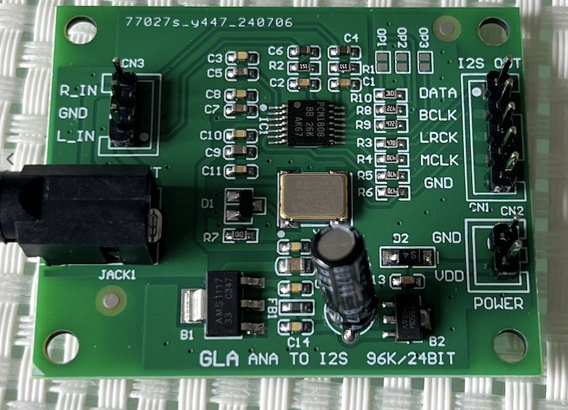
One could use a TVP7002 chip to capture analog video to 24/30 bit RGB data (it digitizes the video for you and extracts the clock), and later I may ultimately build a board to do that with this device, but in the short term in order to prove out the general concept and to evaluate performance I think I can use a couple of Adafruit breakouts to more rapidly try out capturing DVI video and some audio.
The first board below from Adafruit converts DVI to LVTTL RGB for you with a TFP401 chip and provides the pixel clock, DE, H&V syncs. It is intended to feed DVI signal into LCD panels over a FPC flex cable but could very easily feed data to the P2 instead. The second board converts the flex cable into a 40 way IDC for simpler signal routing to the P2-EVAL breakout headers without needing a dedicated board made to do it. I'll just split the 40 way cable into different groups to distribute it to the different 8 bit IO headers.
https://www.adafruit.com/product/2219
https://www.adafruit.com/product/4905
I'm expecting that if I wait on each pixel clock transition in the P2 and then sample the input port data at the right time in a tight 5 instruction loop think I should be able get the P2 to sample pixel rates in the order of 25-30MHz or so and then get the 24 RGB data packed into HUB RAM according to some PASM2 snippets I messed about with. From there it should be possible to stream to SD in 4 bit mode if @evanh 's code can achieve those sorts of speeds using a fast SD card (TBD). We'd need something in the vicinity of 31MiB/s for recording 30Hz 720x480 data. Any captured audio will also add a little more bandwidth to this too. In fact I'm planning to try an I2S ADC capture from a stereo analog audio source, although using the P2 ADC might also work for testing the concept. Syncing audio and video is important and would likely be another hurdle to figure out given the clock source for video and audio are not locked and some sort of elastic fifo during playback may be required with occasional excess samples dropped or repeated as needed to maintain a constant sample playback rate per frame... TBD.
Using such a setup I could then try to play back video into the TFP401 board from a PC or RasPi for example and capture it on the P2. Initially this would be a DVI only solution but I've found front end devices that can strip audio from HDMI and also output to DVI which may be one way to get real HDMI material captured and simple access to the audio.
https://www.auselectronicsdirect.com.au/hdmi-to-dvi-d-video-and-audio-converter
For the TVP7002 approach you could use an HDMI to YUV or RGB converter box to do this too. Those devices are readily available and would provide the audio as well.
I've just ordered the two boards from Adafruit today and when I get them next week I'll start to try out some experiments.
Comments
Here's a quick snippet showing a basic capture loop which should be able to keep up with the captured pixel data if the P2 is clocked at least 10x higher than the incoming pixel rate. The code assumes incoming RGB data on port A and that CLK/DE/VSYNC/HSYNC inputs are available for monitoring the frame state. Another cog would need to read back this captured data from hub RAM and also convert to packed RGB format instead of the captured 32 bit format in order to compress the data before writing to the SD card to reduce the bandwidth needed by ~25%. Fifo blocks would be managed so one scan line could be captured by one cog while a different scan line is processed by another, and some type of SD buffer structure could be filled so sectors would be streamed out continuously per frame. In parallel to this stereo audio would be captured and synced to the start of the frame (COGATN?) and loaded into audio sectors at the end of the frame's RGB data. If the SD card and driver code could keep up with the incoming rate without extended delays then no PSRAM would be needed for intermediate buffering. I think this approach might then be viable.
init ' TODO: setup selectable events 0,1,2 for this cog ' TODO: setup initial fifo write pointer frameloop waitse2 ' selectable event 2 is HSYNC rising/falling as needed ' TODO: check vsync pin state, do ATN to notify new frame begin or end? wait_ready waitse0 ' selectable event 0 is falling edge of clkin signal mov rgb, ina ' get rgb pixel data jnse1 #wait_ready ' selectable event 1 is DE being high wflong rgb ' write to HUB via fifo rep #@.endloop, #0 ' repeat until pixel data becomes invalid waitse0 ' wait for next pixel clock falling edge mov rgb, ina ' get rgb pixel data testb rgb, #DE wz ' check if DE pin still valid if_z wflong rgb ' write to HUB via fifo if_nz jmp #.endloop ' exit the loop when DE is low .endloop ' TODO handle any hsync related stuff with fifo buffering, notify other cogs of scan line buffer ready etc jmp #frameloop ' repeat the outer loop rgb res 1Just feed composite video into the P2 ADC? https://forums.parallax.com/discussion/comment/1529033/#Comment_1529033 Currently monochrome only. Although I think that if you play back the raw signal to a composite monitor you will get color. Basically P2 + SD = D2 recorder. In the past I did capture everything, now the code crops the blanking interval away. It should be easy to adapt my code to capture 480i RGB or YCrCb. The hub has bad congestion when writing bytes at 12.7MHz so I write longs already.
From the TVP7002 you could reduce data rate by another 33% using 4:2:2 YCrCb sampling. (16 bpp but the U and V is shared between 2 pixels.) Some chips like the TVP5150 only output YCrCb format. The only problem is the P2 video hardware doesn't natively handle subsampled YUV.
YUYV-style 4:2:2 is suprisingly easy to expand to the kind of 4:4:4 P2 would need, as noted in the other thread (though I think the code there is wrong and flips the Y pairs). Since P2 normal video is $RRGGBBxx, YUV would be $VVYYUUxx (for analog the channel order doesn't matter because you can rotate the CSC matrix, but for HDMI it is fixed as such)
I plan to start out with simple pure uncompressed RGB initially. Maybe subsampling can come later if required but I'd like to see how much the SD card bandwidth can be pushed and if it can be sustained reliably for the capture and replay.
Another idea I had recently was to try out of those HDMI to CSI-2 capture boards for the RasPi if it is easy enough to get the actual pixel data at SDTV type resolutions into a framebuffer after that for storage on an SD card and muxed with audio, instead of encoding to h264 which the P2 would have no hope of playing. However in the end I think it'd be better to use the P2 to do the actual capture as you then have full control of the entire code and don't depend on any closed source stuff / limited functionality from third parties, and there's probably much less code to write that way as well.
I went back and looked at your code in the other thread @Wuerfel_21 . If a board was designed specifically to capture 4:2:2 format it could direct the YUV data into these byte positions and your tight code could be made to work (effectively taking 5 clocks per pixel for the transformation), otherwise movbyts can be used to put the data where we need instead with one additional instruction in the loop (6 clocks per pixel).
For compression from two separate VVYYUUxx formatted pixel long values (the "a" and "b" regs below) into VVYYUUYY 4:2:2 format it seems like we may be also able to do it in 11 clocks per pixel pair by just simple decimation of every second U/V pair.
compress422
' todo: init fifo ptr and ptrb/ptra prior to this
' compresses at a rate of ~2 pixels in 11 p2 clocks
    mov loopcount, ##600
loop
    rep @.inner, ##512
    rflong a
    rflong b
    getbyte b,b,#2
    setbyte a,b,#0
    wrlut a,ptrb++
.inner
    setq2 #(512-1)
    wrlong 0, ptra++
    djnz loopcount, #loop
    ret

a   long 0
b   long 0
loopcount long 0
Averaging between two pixels U & V values could perhaps give a nicer result but likely is prohibitive in clocks required - or maybe the pixel mix ops could average U/V components quickly like in this code below? Pity we can't find another clock cycle to keep it within 10 clocks per pixel with a clever rolbyte or something. It seems to be 11 clocks right now.
compress422 ' todo: init fifo ptr and ptrb/ptra prior to this and setpix ' compresses at a rate of ~2 pixels in 22 p2 clocks ! mov loopcount, ##600 loop rep @.inner, ##512 rflong a rflong b getbyte y0,a,#2 getbyte y1,b,#2 mixpix a, b setbyte a,y0,#2 setbyte a,y1,#0 wrlut a,ptrb++ .inner setq2 #(512-1) wrlong 0, ptra++ djnz loopcount, #loop ret a long 0 b long 0 y0 long 0 y1 long 0 loopcount long 0Isn't RDLUT 3 cycles and WRLUT only 2?
Also, if the fast block write start address is not long-aligned then bytes in hub RAM longs will be rotated compared to LUT RAM. I haven't checked but Y/U/V in different bytes in cog/LUT longs might perhaps save an instruction somewhere.
.> @TonyB_ said:
Yeah and I try to avoid RDLUTs for that reason. It's mainly RFLONGs and WRLUTs for these pixel transformation processes, plus the block write back to hub.
Interesting idea, it might possibly have some legs if it won't add too many extra cycles in the block transfer. It'd be nice to keep the packed pixel processing work to be 10 or less P2 clocks per pixel so it won't exceed the time we have per pixel on each scanline assuming DVI/HDMI timing or at least the 10x sysclk to pixel clock ratio we'd need for capture data sampling. In fact during playback we'd likely need some more cycles left over for doing other things during the RGB or YUV expanding process like setting up the write requests to PSRAM and for any OSD overlay to be added. For 4:2:2 to 4:4:4 conversion or simple RGB 24->32 bit expansion it appears that should be the case.
I make the inner loops 10 and 21 cycles, not 11 and 22, which is why I mentioned RDLUT vs WRLUT.
Unaligned fast block writes could add only one cycle. It's a general method of rotating data by 8, 16 or 24 bits without using a rotate instruction for each long. It helps if one byte per long is don't care.
Don't forget about that write back to hub RAM in the block transfer at the end which adds another clock cycle for the compressed 4:2:2 pixel pair. I've aggregated away all of the one time setup overheads in the per pixel count too hence that tilde. It's going to become very close over 512 transfers however.
Cool. Sounds potentially useful then.
Following on from the Console Emulation thread discussion regarding HDMI audio issues and also video capture in this thread I've been able to use my Adafruit TFP401 board to capture @Wuerfel_21 's video driver output. I'm seeing good captures now.
Here's the setup:
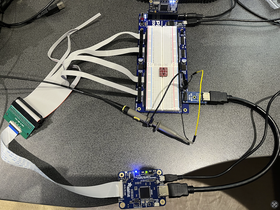
I'm using a PSRAM based P2-Edge with the JonnyMac board and driving HDMI out on P32-P39. The TFP401 board then converts this into parallel RGB24 LVTTL levels, along with a pixel clock, DE, Vsync, Hsync and TMDS "active" signals (indicating valid DVI/HDMI input is present) and feeds back via flat flex cable to a breakout and several IDC ribbon connectors back to the JonnyMac board. Despite the cable length and lack of multiple ground wires thankfully the signal integrity is still okay (it's only clocked at ~33MHz). The Adafruit board nicely has 33ohm series termination resistors present in each signal line which could help a little too.
I'm sending out video colour bars and an audio tone test pattern with the Wuerfel_21 test video driver. The code can also capture back the 32 bit port A data to HUB using the FIFO and then writing it into PSRAM. This is being done at the input rate by waiting for each pixel clock falling edge before sampling "ina" in the COG. This wait for clock low step should allow external HDMI sources to be captured also as long as the COG is clocked at least 10x higher than the pixel rate so my inner loop can run. For 27MHz based video signals this is not a problem on a fast 270MHz+ P2.
When I examine the captured data I see expected 8 bit output values on each RGB channel for the 10b symbols such as preambles, data guard and video guard pattens. With the TERC4 symbols that carry data in the data islands each will uniquely map to a 10b code and this then generates a 8 bit pixel "colour" identifiable on each channel using regular 10b->8b mapping rules. The best part of this TFP401 chip is that DE is signalled active high during the data islands by the TFP401 (wasn't sure if this was going to be the case as it's sort of a DVI only device), and I can see these TERC4 "colours" appearing on its output port as RGB24 codes which can be captured and remapped to 4 bit codes and deciphered.
Here's a capture of the codes actually being sent out the HDMI port and just captured internally without the TFP401 involved. It shows an audio packet being sent out in a data island.
And below is a 32 bit wide capture from the TFP401 of the same type of audio packet showing 8 bit "colour" outputs on each RGB lane. If you look at the blue channel's RGB value above in the right most column set you will see it matches the sequence I captured on the blue channel below. This sequence carries a 24 bit packet header + 8 bit ECC for a stereo audio packet sample being sent in a data island, with the 24 bits data=$000302 and ecc=$80. The red and green channel data values here will differ from above because the actual audio sample packet content is different between the two captures. But the set of 8 bit symbols they use does come from the set of 16 TERC4 values expected so it looks like good data and not random nonsense. I'm really happy about this result. Next up is to add saving to PSRAM for this new capture type and feed some real external HDMI with audio from a Raspberry Pi and capture that to see how it looks on my software decoder. It should finally show what the audio Infoframe and SPDIF status channel data has to say about the audio and what we are missing in our software version on the P2 that prevents a plasma TV and AVR from accepting them.
I've now modified my TMDS decoder software so it can dump out decoded 32 bit RGB pixel + control flag log files captured from port A of the P2 and saved to a uSD card.
After connecting the TFP401 board to my RasPi400 HDMI interface I just captured 30MB worth of pixels to a file. It's essentially a frame grabber setup now. I already programmed the EDID on this capture board which is now emulating my Plasma TV EDID and the RasPi is configured to output a 576p50 PAL TV style video resolution which works fine on my TV.
When examining the decoded log file so far the RasPi is only sending alternating Video InfoFrames and a "Source Product Descriptor" InfoFrame type which I've hand decoded below. At the 864x625 total resolution captured with 32 bpp each frame takes just over 2MB so the 30MB total capture file size contains about 14.5 frames. I see 28 InfoFrames in total so it seems they arrive once per frame, and they come together in the same data island 32 bits apart.
So far not seeing any audio related packet stuff arriving. I think I probably need to play back some audio to make that happen. Right now I can't see my GUI so it's a bit hard to control the Pi. I think I might be able to include my own video driver in the code in order to playback a frame buffer held in PSRAM to the unused HDMI output on the P2 Edge. The PSRAM should have enough bandwidth to be able to store in 108MB/s and also readback at the same rate when the P2 is clocked at 337MHz or so. May have to give the capture COG PSRAM priority which may mess up the playback COG a little and I'll need to use the skew feature to account for inactive pixels per scan line. But it should give me a screen to control the Pi at least so I can trigger it playback audio etc. Otherwise I'd need to introduce HDMI splitters etc but don't really want to as they may muck around with the HDMI signals.
❯ grep Decoded -A 3 -B 1 out
535730 Data:-> TERC4 0001_0000_1100 V- H- 01011010 01011011 01101101 10010
TERC4 Packet Decoded:
Pkthdr: 0D0282 ECC=E4 ComputedECC=E4
Subpkt0: 00001104181230 ECC=AD ComputedECC=AD
Subpkt1: 00000000000000 ECC=00 ComputedECC=00
535762 Data:-> TERC4 0001_0110_1001 V- +H 01011010 10010010 01001011 10010
TERC4 Packet Decoded:
Pkthdr: 190183 ECC=64 ComputedECC=64
Subpkt0: 6364616F724293 ECC=8B ComputedECC=8B
Subpkt1: 6F656469566D6F ECC=7D ComputedECC=7D
1075730 Data:-> TERC4 0001_0000_1100 V- H- 01011010 01011011 01101101 10010
TERC4 Packet Decoded:
Pkthdr: 0D0282 ECC=E4 ComputedECC=E4
Subpkt0: 00001104181230 ECC=AD ComputedECC=AD
Subpkt1: 00000000000000 ECC=00 ComputedECC=00
1075762 Data:-> TERC4 0001_0110_1001 V- +H 01011010 10010010 01001011 10010
TERC4 Packet Decoded:
Pkthdr: 190183 ECC=64 ComputedECC=64
Subpkt0: 6364616F724293 ECC=8B ComputedECC=8B
Subpkt1: 6F656469566D6F ECC=7D ComputedECC=7D
Here is the Video Infoframe content I quickly hand decoded below. Seems to make sense for 576p RGB signal.
TERC4 Packet Decoded:
Pkthdr: 0D0282 ECC=E4 ComputedECC=E4
Subpkt0: 00001104181230 ECC=AD ComputedECC=AD
Subpkt1: 00000000000000 ECC=00 ComputedECC=00
Subpkt2: 00000000000000 ECC=00 ComputedECC=00
Subpkt3: 00000000000000 ECC=00 ComputedECC=00
Video Infoframe packet
Version:2
Length :13
Chksum :30
Data: (LSB First) 12 18 04 11 00 00 00 00 00 00 00 00 00
12 0_00_1_00_10 RGB, active format AR present, no bar, underscanned
18 00_01_1000 No colorimtery, 4:3, Same as Picture aspect ratio
04 0_000_01_00 IT=0 no itc data, Rec601, limited range RGB, no scaling
11 0_0010001 VIC=17 576p50
I also get this SPD InfoFrame which seems to contain a ASCII vendor+product string called "BroadcomVideocore" which makes sense I imagine for a RasPi.
TERC4 Packet Decoded: (Source Product Descriptor InfoFrame)
Pkthdr: 190183 ECC=64 ComputedECC=64
Subpkt0: 6364616F724293 ECC=8B ComputedECC=8B
Subpkt1: 6F656469566D6F ECC=7D ComputedECC=7D
Subpkt2: 00000065726F63 ECC=60 ComputedECC=60
Subpkt3: 00000900000000 ECC=14 ComputedECC=14
?BroadcomVideocore
I just wrote a quick command script to extract the RGB pixels from the captured log and copy into a PPM file. It's kind of a roundabout way to do it vs outputting directly from the decoder but it worked and shows the captured image from Pi400 into the TFP401 is good. You can see I'm running Ubuntu on the Pi400. It's a little slow with Ubuntu but it manages. Will have to overclock it someday.
Also here's the ppm.c program I hacked up to read in 24 bit hex RGB data for each pixel. The updated tm.c decoder program is also attached - still rudimentary/hacky but it sorta works for now.
#include <stdio.h> #include <stdlib.h> int main(int argc, char **argv) { int pixel; int linepixels=0, lines=0; int width, height; width = atoi(argv[1]); height = atoi(argv[2]); printf("P6\n"); printf("%d %d\n", width, height); printf("255\n"); while (scanf("%6x", &pixel)==1) { putchar((pixel>>16) & 0xff); putchar((pixel>>8) & 0xff); putchar(pixel & 0xff); if (++linepixels == width) { if (++lines == height) break; linepixels = 0; } }; return 0; }Mmmh, limited range RGB. I always wonder why that was ever added to the spec, it only purpose seems to be to cause headaches when it's not correctly matched.
But good that the capture is working! I think the Pi's audio can be switched between HDMI and the analog jack, perhaps it's set to the latter.
Wow I just checked in on this after a week or so laying too many carpet tiles. Great progress!
Thanks Lachlan. Yeah it turns out this TFP401 board has been a good buy in the end for this project and glad I didn't need to go make a PCB just to get something up and running initially.
I also received those two I2S ADC boards from AliExpress I was mentioning to you a while back with the Texas Instruments PCM1808 chip. Haven't tried them yet as I might now be able to capture PCM audio from the HDMI bitstream when unencrypted. Until I knew it was possible to decode HDMI from this Adafruit board, I was just planning to use DVI and capture stereo audio using the PCM1808 into the P2.
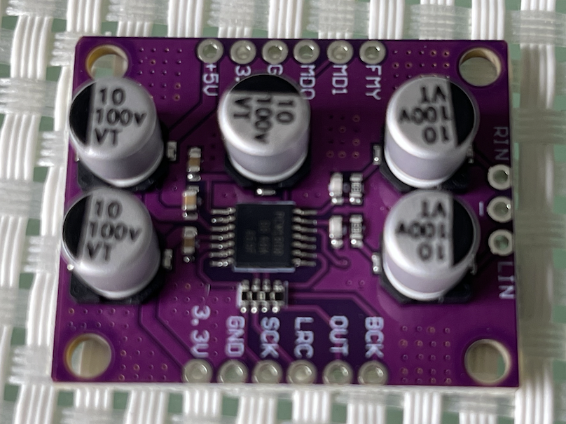
This was the link to the green board that looked more interesting as it already has a crystal on board and only needed 3 pins on the P2 side when run in its master mode, instead of 4.
https://www.aliexpress.com/item/1005006141604047.html
Yeah I'm pretty happy that data is not corrupted. The audio shouldn't be set to analog as it was last hooked up to my Plasma and running ok, but perhaps it switched back when flipping HDMI cables, or needs a first playback after reboot to activate it. I plan to try to show the Linux GUI on the P2 HDMI via PSRAM and my own video driver today if possible so I can at least control the Pi400, no doubt syncing will be a slight problem as the P2 is running at 337MHz instead of 270MHz. Whatever, I only need some jittery/tearing image to control this Pi400 desktop environment and setup/output audio etc. There's probably remote ways to login with SSH and install audio etc but why do that when you can just playback from PSRAM.
I just thought about an interesting application for Roger's capture setup: fully objective latency measurement of interactive audio/video systems.
Basically, you'd emulate a USB HID device and connect it to the device under test, which is also connected on the HDMI input. To run a test some signal (i.e. a button press or mouse movement) is sent through the HID device and the subsequent couple frames of video/audio data are captured (along with relative timing of the USB events). Analyzing the results would lead to very interesting data. I have the very well founded suspicion* that many games have extra unnecessary latency either inherent in their programming or get saddled with it by the operating system (tendencially increasing amounts as the APIs used become more and more legacy over time). Maybe I have to grab one of these TFP401 boards.
*: Some time ago, I have discovered to my shock and horror that D3D9 on Wine has added latency by default. You basically have to put a dxvk.conf into your game install folder to the extent of the below, otherwise you are not going to have a good time with, I want to say anything fast-paced, but even the mouse cursor in Fallout NV feels terrible without this.
Good idea.
Go for it - they're cheap and effective for capturing SDTV stuff and if you have a JonnyMac or P2-EVAL all you really need to do is make a simple harness, although I did need to flip the IDE connector as well on that RasPi breakout BTW because of the pin order on the cable, otherwise bit reversals would be needed.
While ideal for STDV/EDTV stuff on the P2 they can actually inherently generate RGB data in video modes up to 165MHz pixel clocks but the P2 async clocking will limit you before this. However with a dedicated P2 board the P2 clock could in theory be synced to the pixel clock (i.e. feed it to XIN) so you could then use a streamer to get some data in to HUB RAM at least, PSRAM can't sustain 32 bits at sysclk/1 without multiple/wider banks. If you could use the PLL with a prescaled input pixel clock maybe you could run sysclk at a multiple of the pixel clock and get to do more capture processing work. The P2 could even be instructed to look for pixels of a certain colour at certain location(s) on screen and detect the delay to that point from some USB event, or you could try to capture it all and offload to a powerful system for all sorts of analysis.
Yesterday I was wondering about capture of high resolution HDMI/DVI sources via the TFP401 and what's possible.
There are three issues here:
Signal integrity: We need to input 28-29 data signals into the P2 operating at the pixel rate with lots of parallel bus transitions causing switching noise etc. I haven't looked into what my own setup can do yet on the ribbon cable, but a better capture board could be layed out to terminate the FPC connector directly using a proper ground plane and giving more ground return paths back to the connector for the number of active signals.
Capture bandwidth: we can capture to hub RAM from streamer directly, and then potentially to PSRAM after that. The hub RAM bandwidth from the pins is massive and we can stream 32 bits at up to sysclk rates, while the PSRAM is more limited to something under sysclk BYTES/sec. Ballpark overheads might be around 10% or so, depending on driver and burst sizes etc. You could in theory have multiple memory banks to increase this, but we already have used many P2 IO pins to capture the data in the first place. PSRAM is very convenient and present on the P2-EC32MB but perhaps on other custom P2 boards two HyperRAM banks would be doable with 11 pins each which could double the memory bandwidth if you split the workload over multiple COGs.
Asynchronous sampling: Without a dedicated board clocked at the recovered pixel rate (see prior post) it is going to be difficult to sample something asynchronously whose pixel rate is operating faster than about 0.1 sysclock if you need to wait for an edge before reliably sampling the pins. My own code doing this below needed 5 instructions (10 P2 clocks) between incoming pixels in order to ping/pong to a hub buffer via the FIFO. I had to unroll a few iterations of the main loop for doing the housekeeping in the capture routine. I also tried a "wflong ina" at one time to try to shave 2 cycles from the loop by avoiding the additional "mov rgb, ina" but it didn't seem to work correctly - maybe I might have been sampling at the wrong time or there is some problem sending INA data directly to the FIFO like this. I should revisit this again sometime if it gets the loops down and helps to boost the capture pixel rate to ~42MHz or so which would support a 800x600p60 capture.
CON
    CLK_PIN = 24
    ACT_PIN = 25
    HS_PIN = 26
    VS_PIN = 27
    DE_PIN = 28

DAT
            orgh
capturecog
            org
            loc     pa, #\wrbuf         ' get double buffer base address
            add     pa, #63
            andn    pa, #63
            loc     ptrb, #\capturing   ' get capture state address
            mov     pb, pa              ' compute address of second buffer
            add     pb, ##BUFFER_SIZE   ' by adding the BUFFER_SIZE to the first buffer start address

            ' setup selectable events 1,2,3 for this cog
            setse1  #384+DE_PIN     ' DE high
            setse2  #64+VS_PIN      ' rising vsync
            setse3  #128+CLK_PIN    ' falling clock


frameloop
            wrfast  numblocks, pa   ' setup initial fifo write pointer

            waitatn                 ' wait for trigger from client
            rdlong  size, ptrb      ' read in size to be captured in bytes
            sets    fbins, #pb      ' prep next buffer ptr in fblock instruction

            pollse2
            waitse2                 ' selectable event 2 is VSYNC rising/falling as needed
            pollse3                 ' selectable event 3 is the clock pin falling

outerloop
            waitse3
            mov     rgb, ina
            wflong  rgb
fbins       fblock  numblocks, pb
            xor     fbins, #1       ' toggle pa/pb in fblock instruction source address for ping/pong buffering

            waitse3
            mov     rgb, ina
            wflong  rgb
            rep     @.inner, xfers3

            waitse3
            mov     rgb, ina
            wflong  rgb
.inner
            sub     size, bufsz
            cogatn  ptra            ' slightly premature notification with one sample left but the PSRAM write will be much slower than this

            waitse3
            mov     rgb, ina
            wflong  rgb
            tjnz    size, #outerloop

            wrlong  #0, ptrb
            jmp     #frameloop          ' repeat the frame capture loop

numblocks   long    BLOCKS_PER_BUFFER  ' number of 64 byte blocks per FIFO ping pong buffer
xfers3      long    BUFFER_SIZE/4 - 3  ' number of 32 bit transfers for second buffer minus 3 for unrolling
bufsz       long    BUFFER_SIZE        ' size of each ping/pong buffer
size        res     1
rgb         res     1
So given all this, I was wondering about my current async capture P2 setup and whether it might be possible to try to use the streamer for capture and sort of oversample the signal and post-process it afterwards. If we know we have say 3 or 4 samples per pixel based on the sysclk we could resample the data at the expected pixel rate (which we could measure first using a smartpin) and write that to memory, saving space and bandwidth. For PSRAM we might be able to get up to 75Mpixels/sec or 720p/1080i type resolutions. Of course this is only going to be useful for a few frames before we run out of memory - even a fast SD card in 4 bit mode won't help us out there. But just a few frames or even one may be useful in some cases. If more time is needed during the capture for resampling perhaps it would be even possible to sample screen data section by section or scan line by scan line if the image is frozen on screen (e.g. paused game or a static GUI) so that you can a capture a stable image. I wonder how tight a resampling process like this could end up and just how many P2 clocks per output pixel sample would be needed and therefore how many COGs could do it...? Ideas are welcome.
I might like to try some of these ideas out although I expect it could end up being IO noise/skew limited in this initial setup. After that I could possibly try to make a PCB to adapt the 40pin FPC connector to a P2-EVAL breakout footprint.
UPDATE: another point to make related to the resampling, is that we also do have the clock pin being sampled. So we might be able to look for a falling edge clock transition in the data and then assume the next sample was valid if we have enough samples per pixel. This could possibly be faster than another numerical resampling approach depending on how many excess samples we end up reading. Perhaps the data might be best FIFO or block read into COG/LUT RAM for processing rather than randomly accessed sample by sample from hub using a moving memory pointer that advances multiple samples at a time from some numeric counter overflow etc. Time will tell.
Here's one PASM snippet for a suggested way we could resample with a phase accumulator. Not fully coded but looks like around 14 17 P2 clocks per generated pixel (including block read and FIFO write but not housekeeping). Not very fast. You'd need 4 5 COGs in parallel doing this to keep up with 75Mpixels/sec at 300MHz+ P2 rate (sysclk >= 4x pixelclocks). EDIT: more like 17 clocks if you are block reading in 4 captured pixels per output pixel.
mainloop
            ' TODO: setup/advance ptra here for reading original captured data
            ' TODO: setup/advance wrfast buffer here, deal with ping/pong buffers as needed
            ' TODO: clear C flag at the start

            setq2   #512-1
            rdlong  0, ptra++           ' block read next 512 longs from hub to LUT
            testb   ptrb, #9 wz         ' get state of ptrb bit 9 into z flag

    if_c    rdlut   data, ptrb          ' read in last iteration data from new block
    if_c    wflong  data                ' write previous iteration's data to HUB

            rep     @.endloop, #0       ' continue until we jump out of rep loop
            add     phase, freqlo wc    ' add to phase accumulator LS part
            addx    ptrb, freqhi        ' add to phase accumulator MS part
            testb   ptrb, #9 xorz       ' test if bit 9 changes and we are wrapping
    if_z    jmp     #.endloop           ' exit before writing
            rdlut   data, ptrb          ' resample
            wflong  data                ' write back to hub via FIFO
.endloop

            ' TODO: set C flag as needed to write first sample in next iteration

            jmp     #mainloop           ' repeat


freqlo      long    NCOFREQ_LS          ' setup these based on the resampling freq ratio
freqhi      long    NCOFREQ_MS
phase       long    0                   ' could adjust this to center sampling of bits
data        res     1
UPDATE: looking into the alternative clock pin change method seems like it'll be a lot slower than the numerical resampling above. For example the tight inner loop of 10 clocks below has to be executed multiple times per output pixel and this is without proper wrap testing.
                    rep     #5, ##512
                    rflong  sample                  ' read next sample
                    testb   sample, #CLK_BIT xorz   ' test clock pin z=1 if changed from prior value
                    testb   sample, #CLK_BIT wc     ' test clock pin c=1 if was a pos edge, c=0 if was neg edge
    if_nc_and_z     rflong  sample                  ' c=0 indicates falling edge, read again
    if_nc_and_z     wrlut   sample, ptrb++          ' write to FIFO
Based on the above I believe that synchronous streamer capture is probably the way to go if you do want a high resolution capture, but it's still interesting to see how far things can be pushed otherwise.
Just noticed on my revB P2-EVAL that there are XI and XO pads exposed on the board. Hmm I wonder if I can safely feed the pixel clock signal from the TFP board to the XI pad with the crystal still fitted?
Will this actually work and then I just define _XINFREQ in the code instead of _CLKFREQ? Does the presence of the 20MHz crystal in this mode do any harm or limit things in any way?
If this works I might be able to do some synchronous capture at higher speeds.
I just tried wiring it in and it seems to work! I know it's running off the XI pin because when I pull the clock signal out of the board's XI pad it changes frequency and affects serial output characters but keeps running. When I plug back it it resumes again.
I sampled INA back to back in a COG (2 clocks/sample) and see a pattern on the CLK pin (bit 24) that repeats every 12 clock cycles as expected. This is cool and I think I can work with it. Hopefully it'll be able to take a 75MHz signal in without too many issues then I could sample 720p/1080i with the streamer.
CON

    _xinfreq = 27000000
    _clkfreq = 324000000  ' 12x pixel clock

DAT
            orgh
samplefast
            org

            mov $,ina
            mov $,ina
            mov $,ina
            mov $,ina
            mov $,ina
            mov $,ina
            mov $,ina
            mov $,ina
            mov $,ina
            mov $,ina
            mov $,ina
            mov $,ina
            mov $,ina
            mov $,ina
            mov $,ina
            mov $,ina
            mov $,ina
            mov $,ina
            mov $,ina
            mov $,ina
            mov $,ina
            mov $,ina
            mov $,ina
            mov $,ina
            mov $,ina
            mov $,ina
            mov $,ina
            mov $,ina
            mov $,ina
            mov $,ina
            mov $,ina
            mov $,ina
            mov ptrb, ptra
            add ptra,#4
            setq #31
            wrlong 0, ptra
            wrlong #1, ptrb ' indicate done
            cogid pa
            cogstop pa
Press Enter to start capture
FE5336CD
FF5336CD
FF5336CD
FF5336CD
FE5336CD
FE5336CD
FE5336CD
FF5336CD
FF5336CD
FF5336CD
FE5336CD
FE5336CD
FE5336CD
FF5336CD
FF5336CD
FF5336CD
FE5336CD
FE5336CD
FE5336CD
FF5336CD
FF5336CD
FF5336CD
FE5336CD
FE5336CD
Tried a synchronous capture of a 1360x768 res image from the RasPi HDMI output using the P2 EVAL XIN pin clocked at 85.5MHz using the recovered TFP401 pixel clock. This is running the P2 hard at 342 MHz (4x pixel clock). Tried out all 4 P2 clock phases when starting the streamer capture with Schmitt trigger input pins on port A. Can't seem to get a perfectly clean capture image as yet. Might be PLL jitter from noisy input lines? Could also be P2-EVAL skew between pins, though I'd hope with 4 phases there'd be an overlap somewhere where the data was fully valid over all bits. 85MHz is ~ 11.7ns period, was the pin to pin skew worse than this? This screenshot portion is probably as clean of the 4 different phases as I could get.

 eg. 85.5Mpixels/sec*3 byte = 256.5MiB/s on a 342 MHz P2. I'll need to take a closer look at the compression code in case it's somehow messing up the RGB pixels. If this would work then the slower 74.25MHz pixel clock should be usable as well for 720p60/1080i60 captures, and the P2 could run at a more sane 297MHz. If this is skew or signal related then a dedicated board with a decent ground plane may be needed.
I am compressing the incoming RGB32 scan line pixel data down to RGB24 for storage and this buys just enough bandwidth reduction to be able to capture the full frame into PSRAM on the fly.
DAT orgh rgbcompressor org ' pass in the address of the input buffer start address and the output buffer address struct to PTRA rdlong pa, ptra++ ' read input buf addr rdlong ptra, ptra ' read output buf addr rdfast #0, pa ' prep input buffer for reading mov pb, #4 * 8 ' 8 scan lines comp_outer mov ptrb, #0 rep @.compressloop, #112 rflong rgb0 ' c0b0g0r0 rflong rgb1 ' c1b1g1r1 rflong rgb2 ' c2b2g2r2 rflong rgb3 ' c3b3g3r3 setbyte rgb0, rgb1, #3 ' r1b0g0r0 * wrlut rgb0, ptrb++ shr rgb1, #8 ' 00c1b1g1 setword rgb1, rgb2, #1 ' g2r2b1g1 * wrlut rgb1, ptrb++ rolbyte rgb3, rgb2, #2 ' b3g3r3b2 * wrlut rgb1, ptrb++ .compressloop ' 22 plus 3 write clocks = 25 clocks for 4 output pixels setq2 #336-1 ' write 336 longs to HUB in a burst wrlong 0, ptra++ ' generates 448 pixels per loop djnz pb, #comp_outer ' repeat until done cogid pa cogstop pa rgb0 res 1 rgb1 res 1 rgb2 res 1 rgb3 res 1Just found a bug in the code above. Fixed and retested and got better results. Need to check other phases again.
Here are the 4 phases.. still not perfect but quite a bit better at least. Waitx #2 is best but I think there is some PLL jitter, if you look you see some scan lines shimmer. Could just be ringing or overshoot in some cases too.
waitx #0


waitx #1
waitx #2
waitx #3
Here's the rest of the non-black items in that login screen with waitx #2. Unfortunately this is not a good capture source as it doesn't have much on screen. I'll have to get it to switch back to this resolution after login instead of 576p50 I was using before.


Here's a full screen HDMI capture of 1360x768 at 85.5Mpixels/s - not too bad but there are some artefacts / noise. Look at the mouse pointer and some of the icons on the left of the GUI. I wonder if a decent PCB will solve most of this... might have to try it.
If you're gonna make a custom PCB for this, I'd most certainly be interested
Me too! I'd love to find a reason to layout an optimal P2 board without all the conflicting compromises, or to acquire one from someone who does have a reason and the resources")
With Ada, that's a panel of 3 locked in !!
Well, there'd be some heavy compromise here... If we need the entire Port A for the capture interface, 18+ pins for PSRAM, 4 pins for SD/flash (do we need flash?), 2 for serial, that would leave exactly 8.
Whereas possible extra wants would be:
Though with an optimized board maybe sysclk/1 HyperRAM can be a thing again and save pins that way... There's a nice-looking part, IS66WVH64M8DBLL, 3.3V 64Mx8