Yeah I guess that solution is at least usable. BOOT0 is essentially just a flash chip disable if held low and doesn't directly control boot order. For a SD boot configuration you'd also need to pull down P61 with an external resistor (probably you should add that pin state as another column in your rev D schematic's boot configuration table), otherwise by default it would boot from flash. If you need to write to flash after SD boot (e.g. unbricking a bad flash image), you can wire P61 with a pull down resistor and let BOOT0 float high, and BOOT1 to float or go low.
Note that PGLED2 may potentially influence boot as well by pulling P59 high and forcing serial boot if this pin is powered and minimal current is drawn from it. That should be checked too to see what it does to boot up.
R4=220ohms? Shouldn't it just be 240 to be safe if that is what P2-Eval & Edge both use? I know it's close, but so was 300 ohms...
@rogloh said:
... BOOT0 is essentially just a flash chip disable if held low and doesn't directly control boot order. For a SD boot configuration you'd also need to pull down P61 with an external resistor (probably you should add that pin state as another column in your rev D schematic's boot configuration table), ...
Right! BOOT0 isn't controlling the boot order. The U1 gate doesn't seem useful. We use SPI clock mode 3 in driver software to cleanly manage operation of both the EEPROM and SD card alternately.
R4=220ohms? Shouldn't it just be 240 to be safe if that is what P2-Eval & Edge both use? I know it's close, but so was 300 ohms...
I'm good with 220 R. Lower is better for performance. The resistor only there as a safeguard in case the SD gets stuck driving its CMD pin until power down.
On that note, a power down control for the SD card would be desirable feature.
Yes, U1 has no purpose currently. I've only kept it in case R27 is not populated, so the module can revert back to its current model of operation where the SD is the default boot source and flash can be booted by connecting an external resistor.
Yes, it is a good idea to include a note about pulling P61 down in the schematic.
Oh, err, just reading more of what Roger has said. U1 is the switch alternative that allows the EEPROM CS to be pulled high without affecting P61 when not booting from EEPROM.
EDIT: I've not looked too hard before. I see what you mean about there not being an easy line of order in the booting. Any one can be forced but that's it.
Maybe not support direct SD booting. Always require a loader in the EEPROM instead. After all, if the EEPROM is enabled at all then SD boot can't happen anyway.
The alternative would be add new hardware to work around this so that an SD boot can still reprogram the EEPROM. This would be something like driving BOOT0 from the Prop2 to engage the EEPROM after boot.
In hindsight, here's what I think would be the good options:
1: Serial interruptible delayed EEPROM boot. SD accessible. (Already supported with P61 pull-up)
2: Serial interruptible delayed SD boot with fallback to EEPROM.
3: EEPROM boot only. SD accessible. (Already supported with P61 pull-up + P59 pull-down)
4: SD boot with fallback to EEPROM.
EEPROM boot with fallbacks aren't very effective options given that once it's bootable the fallback can't happen.
EDIT: Hmm, if we accept not having a pull-up on EEPROM CS pin then it's possible to have SD boot and still access to the EEPROM. This would need software support to recognise that P61 needs driven high ASAP after boot. Oh, Smile, I suspect the ROM SPI routines using clock mode0 will cause a conflict if both SD and EEPROM are connected at boot time.
It's an either-or situation I think. Either support SD booting or support EEPROM booting.
@rogloh said:
Note that PGLED2 may potentially influence boot as well by pulling P59 high and forcing serial boot if this pin is powered and minimal current is drawn from it. That should be checked too to see what it does to boot up.
It won't. It is intentionally white LED, and its forward voltage is around 3V or more, so unless the line is pulled high elsewhere, P2 will never see high from the LED alone
@evanh said:
It's an either-or situation I think. Either support SD booting or support EEPROM booting.
Not happy with that. I want to support both and with minimum external requirements.
There is one universal sequence, which will not require any bootstrapping at all: serial (100ms)->SD->flash->serial (60s)->shutdown.
In fact, I am not even sure what the 60s window is used for. 100ms should be more than ehough for automated upload from any IDE, and in a stand alone situation with pre-loaded firmware, a boot from SD would take precedence. So the 60s one may even disappear.
This can be done with reasonably simple external logic, but the only problem is how to know when P2 is running valid firmware.
@knivd said:
There is one universal sequence, which will not require any bootstrapping at all: serial (100ms)->SD->flash->serial (60s)->shutdown.
That one doesn't exist as a single option though. Closest is: serial(100ms)->flash->serial(60s)->shutdown.
Serial booting via another microcontroller has been done also. This has the advantage of freeing up pins P58..P61.
The only way to have SD booting is to exclude the EEPROM entirely. Without external switching, it would be inaccessible even after boot.
It is possible to EEPROM boot with post-boot SD access ... but this config is risky due to SPI cmode0 clocking will incorrectly select both devices during boot, I think - Not tested by me but I do know others have had issues with cmode0 which resolved by changing the drivers to use cmode3 when sharing both devices.
maybe switching power off of SD (sort of needed if SD hangs after reset) with a pin could solve the boot issue also. No power, no SD, no conflict, just guessing.
@knivd said:
In fact, I am not even sure what the 60s window is used for.
Oh, that's for user terminal access. There is key codes for bringing up an interactive debugging monitor or the built-in Taqoz Forth. I've barely used either myself.
@msrobots said:
maybe switching power off of SD (sort of needed if SD hangs after reset) with a pin could solve the boot issue also. No power, no SD, no conflict, just guessing.
This is needed too but not sure it would make a combined boot any more reliable.
Looking at the ROM booting code ...
'
' SPI long/byte out
'
spi_cmd8    mov pa,#8           'ready to send 8 bits

spi_cmd     drvh    #spi_cs         'cs pin high
        rol pb,#24          'msb-justify byte
        drvl    #spi_cs         'cs pin low

.out        rol pb,#1       wc  'get bit to send
        drvc    #spi_di         'drive data-in pin to bit
        drvh    #spi_ck         'drive clock pin high
        drvl    #spi_ck         'drive clock pin low
    _ret_   djnz    pa,#.out        'loop to output bits, return when done
'
'
' SPI byte in
'
spi_in      rep @.in,#8         'ready to input a byte
        drvh    #spi_ck         'drive clock pin high
        drvl    #spi_ck         'drive clock pin low
        testp   #spi_do     wc  'sample data-out pin ('testp' is from before 'drvh')
        rcl x,#1            'save data bit
.in
        ret
The low level SPI clocking is using CPOL=0 of cmode0 ...
'+-----------------------------------------------------------------------------+
'+      SD SPI Send/Recv Routines... (write/read byte/long simultaneously)     +
'+              /CS=0 & CLK=0 on both entry and exit                           +
'+-----------------------------------------------------------------------------+
_recvlong       neg     dataout,          #1            ' call here to Recv a Long (+send 1's)
_sendlong       mov     bitscnt,          #32           ' call here to Send a Long (long=32bits)
                jmp     #@_sendrecv                     '
_sendFF                                                 ' call here to Send $FF Byte
_recvbyte       neg     dataout,          #1            ' call here to Recv a Byte (+send 1's)
_sendbyte       rol     dataout,          #24           ' call here to Send a Byte (msbit first)
                mov     bitscnt,          #8            '                          (byte=8bits)
_sendrecv       mov     reply,            #0            ' clear reply
' 8+15 low/high clk cycles (8.7MHz@200MHz, 1.3MHz@30MHz)
.nextbit        rol     dataout,          #1        wc  ' \ prepare output bit (DI=0/1)..
                outl    #sd_ck                          ' | CLK=0  (already 0 first time)
                outc    #sd_di                          ' / write output bit: output on CLK falling edge
                waitx   #2                              ' |   setup time to be safe
                outh    #sd_ck                          ' \ CLK=1
                waitx   #3                              ' |   setup time to be safe
                testp   #sd_do                      wc  ' | read input bit:   sample on CLK rising edge
                rcl     reply,            #1            ' / accum DO input bits
                djnz    bitscnt,          #.nextbit     '   8/32 bits?
        _RET_   outl    #sd_ck                          ' CLK=0 on exit
'+=============================================================================+
And same for low level SD SPI using CPOL=0 as well.
Another option (which I didn't mention before as I didn't want to complicate things further but that seems to have probably already happened), is to tie the Card Detect pin from the uSD socket to another P61 pulldown resistor. That way the presence of the card itself can determine/override the boot order too and could work for a flash upgrade/unbricking case from uSD. However you may not always want this because you may wish to boot from flash and then use the uSD for other runtime resources, so you may still need a way to override the order somehow. Consider this...
With different resistances values seen on P61 you could have four things working:
1. no card fitted, normal flash boot (P61 pulled high very weakly internally with 100k)
2. card fitted, card detect ground pulls weakly low on P61 with another resistor ~30k? (this overrides 100k), uSD boots
3. card fitted, P61 additionally pulled high with ~10k externally to override card detect pulldown resistance and let flash always boot even with uSD fitted
4. card not fitted, and no flash boot ever desired even if card not present, 10k external pulldown on P61.
EDIT: I may try to draw a picture of this when I get back later...it'd be nice to incorporate this into the BOOT0 pin state too and have both pins strapped to H/L/F to select everything, if possible. That would also avoid external resistors on these pins.
@evanh said:
The ten high speed connections to the hyperRAM really should be completely excluded from the off-Stamp I/O. That frees up the NORAM contact as well. Redistribute those contacts to increase ground count and maybe have four VIO supply contacts, one for each side of the Prop2.
@rogloh said:
2. card fitted, card detect ground pulls weakly low on P61 with another resistor ~30k? (this overrides 100k), uSD boots
Now just have to test out reliability of booting with both devices selected because of CPOL=0.
EDIT: Ah, it could be alleviated by moving the inline 220 R resistor, R4, on P58 from the SD's MISO pin to the EEPROM's MISO pin. This would give the SD card driving strength priority over the EEPROM and thereby allowing SD boot with the EEPROM still accessible later.
This would also exclude Roger's option 3 above since attempting boot of EEPROM with an SD card inserted would jam the MISO pin with SD state info.
It's unknown if this might corrupt the EEPROM still but a small boot image on the SD card would be the way to limit such risk. Then have a second stage loader that changes to CPOL=1 (cmode3).
@evanh said:
The ten high speed connections to the hyperRAM really should be completely excluded from the off-Stamp I/O. That frees up the NORAM contact as well. Redistribute those contacts to increase ground count and maybe have four VIO supply contacts, one for each side of the Prop2.
You could test how much effect there actually is, by removing contacts from a socket on those pins
I'm still in a mind to solder wires to the Stamp instead of using a socket.
@rogloh said:
Another option (which I didn't mention before as I didn't want to complicate things further but that seems to have probably already happened), is to tie the Card Detect pin from the uSD socket to another P61 pulldown resistor. That way the presence of the card itself can determine/override the boot order too and could work for a flash upgrade/unbricking case from uSD. However you may not always want this because you may wish to boot from flash and then use the uSD for other runtime resources, so you may still need a way to override the order somehow. Consider this...
It is a very interesting idea. I did not think about using the card detect to override the boot sequence. Deserves a proper thought.
@evanh said:
I'm still in a mind to solder wires to the Stamp instead of using a socket.
Or you can convert it to a through-hole module by soldering 1.27mm headers into the holes on it. It is an option which might be useful in specific situations
@rogloh said:
Note that PGLED2 may potentially influence boot as well by pulling P59 high and forcing serial boot if this pin is powered and minimal current is drawn from it. That should be checked too to see what it does to boot up.
It won't. It is intentionally white LED, and its forward voltage is around 3V or more, so unless the line is pulled high elsewhere, P2 will never see high from the LED alone
Please note that a floating LED is also a photovoltaic cell. It converts light to electric energy. The surface of a 0402 LED is tiny but the load of an open CMOS input without any pullup/down resistor has a very high impedance. So shining light onto the LED may actually pull P59 low!
@ManAtWork said:
Please note that a floating LED is also a photovoltaic cell. It converts light to electric energy. The surface of a 0402 LED is tiny but the load of an open CMOS input without any pullup/down resistor has a very high impedance. So shining light onto the LED may actually pull P59 low!
Technically, it might just as well as strong electromagnetic pulse, voltage spike or number of other things. It is not however something that I believe would be a factor in real world applications.
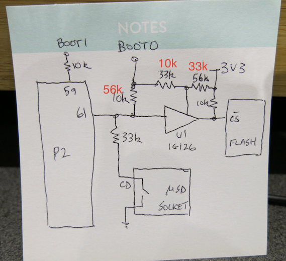
Here's the idea I had. Still not 100% perfected and needs some resistor value tweaks but probably gets the idea across. Relies on resistor values that guarantee CMOS 3.3V logic thresholds are met in different cases.
BOOT1 is the same signal as exists today (a 10k resistor to P59). BOOT0 is new. Other signals not shown for brevity.
If you float BOOT1 the following applies (and a serial connection can still override the boot source within 100ms of reset):
Strap BOOT0 high - forces Flash boot, runtime can access flash and uSD when fitted
Float BOOT0 - boot depends on whether uSD fitted or not, if fitted will boot from uSD, if not fitted will boot from flash (flash should still be accessible in these two cases but needs better resistor values chosen to keep U1 1G126 gate enabled when BOOT0 floats and P61 is driven low, that's the broken bit I see right now, hopefully other resistances can fix it)
Strap BOOT0 low - forces SD boot when card is fitted, no flash access at runtime
If you strap BOOT1 high you force serial boot only
If you strap BOOT1 low you prevent the serial access override of 100ms after reset, and above logic in BOOT1 float case still applies
EDIT:
This rearrangement of resistance values in red may work better, still checking it:
Update: no, I think it upsets the BOOT0 strapped high case and makes it behave the same as if it was floating where uSD presence overrides flash even when we want to boot from flash. Will keep on looking...
Update2: changing the lower 33k resistor attached to card detect to 82k and keeping the red values as well I think works but it's a bit tight. There will be better values I'm pretty sure...
Do not try to boot from EEPROM with SD card inserted.
When the EEPROM is switched in (U1 enabled), the SD card will never be able to boot. SD as a fallback is broken. This happens because of dual device selection from clocking mode of Prop2 ROM. The SD card can also lock up because of corrupted commands during EEPROM boot attempt.
Also, with R4 on the SD slot, EEPROM MISO overpowers the SD MISO during boot.
PS: This will apply to the Edge and Eval Boards too. Because of the SPI clock mode in use, EEPROM booting will mess with any resident SD Card.
When the low level ROM routines were written, I don't think very many people understood that cmode3 was a viable alternative to cmode0. It wasn't a concern prior to sharing the SPI bus in this manner. So it looks like the Eval Board design was intended as an either-or one. Either EEPROM is switched in and SD slot left unused, or EEPROM is switched out and SD card is slotted.
How about using a PLD chip with P57, after boot, as its load signal for a chip select number. Then any one SPI device can be selected at a time. Existing software will need to be modified to manage it obviously. Currently, there is a mix of software that does and doesn't use cmode3 anyway. Things need a tidy up.
During boot one SPI device is selected, by the PLD, as per BOOT0.
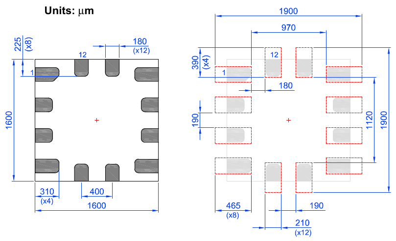
Here's package/footprint of example Renesas SLG46108 PLD with 6 I/O pins:
@evanh said:
Do not try to boot from EEPROM with SD card inserted.
When the EEPROM is switched in (U1 enabled), the SD card will never be able to boot. SD as a fallback is broken. This happens because of dual device selection from clocking mode of Prop2 ROM. The SD card can also lock up because of corrupted commands during EEPROM boot attempt.
Also, with R4 on the SD slot, EEPROM MISO overpowers the SD MISO during boot.
PS: This will apply to the Edge and Eval Boards too. Because of the SPI clock mode in use, EEPROM booting will mess with any resident SD Card.
When the low level ROM routines were written, I don't think very many people understood that cmode3 was a viable alternative to cmode0. It wasn't a concern prior to sharing the SPI bus in this manner. So it looks like the Eval Board design was intended as an either-or one. Either EEPROM is switched in and SD slot left unused, or EEPROM is switched out and SD card is slotted.
Hmm, I had (possibly naively) believed the pin logic had all been figured out during the P2 boot code design phase with CLK and CS flipped so that both devices could be fitted and one would get activated while the other was disabled (or only temporarily activated without any clock pulses so as not to drive the shared data bit pin at the time it was being sampled and the series resistor was there to account for this). Wasn't that the original intent? Didn't realize it was actually broken and only one could be attached at a time. Makes sense as to why P2-EVAL has a physical DIP switch to isolate the flash CS pin. If this is the case it would mean that upgrading/restoring P2 flash in the field from an emergency SD boot operation may not not actually be possible and true bricking is always a potential reality. Disappointing... P2 and SD is a bit of a PITA really. Quite a set of limitations. I think ke4pjw also suffered from various SD problems too.
@evanh said:
How about using a PLD chip with P57, after boot, as its load signal for a chip select number. Then any one SPI device can be selected at a time. Existing software will need to be modified to manage it obviously. Currently, there is a mix of software that does and doesn't use cmode3 anyway. Things need a tidy up.
During boot one SPI device is selected, by the PLD, as per BOOT0.
Interesting idea to use a small part as a mode-cleanup manager.
A small MCU with a LOGIC block could also be a good candidate.
I see the EFM8BB50 showing a QFN12 2x2 package, and it does have a CLU, but it was announced in March, then went back into stealth mode ? (bigger parts are available in 3x3 package)
Some other MCUs come in 2x2 ballpark packages, but I cannot see LOGIC blocks in them.
Couldn't this problem be rectified by taking a lesson from the Prop1 such that the Prop2 will always bootup by first checking the serial port for 100ms, and failing that always boot from flash? Then, you could have an SD Card bootloader within flash that could be executed to continue the bootup sequence from the SD Card.
Granted, you would have to write the SD Card bootloader code to serve as a Secondary Loader programmed into the flash (just like the Prop1 has it stored in EEPROM), but it seems doable. Being able to bootup using Serial would allow you to load new code into the flash chip thus avoiding the bricking problem.
The flash and SD Card could probably share the same clock, SI, and SO signals, but the CS pin for each one would have to be chosen to avoid having the P2 ROM bootup activating both at the same time. That probably rules out using P61 and P60. Maybe keep P61 for the flash but something like P57 for the SD Card. This would mean a re-spin of the P2_STAMP design, but it looks like it's heading there anyway.
I must admit that I hate the DIP switch setup on my P2 Evaluation boards. I wish Parallax had settled on the Prop1 technique wherein bootup attempt starts with Serial and then Flash, with the option of having a Secondary Loader execute from there to read the SD Card.
100 ms serial+flash always work. Having an external ram allowing SD loader resident in flash. I don't have the P2 Stamp, but as far as I know it has Hyperram onboard.
So the solution for EC32 or this board may be something like this: it starts from the flash. It checks for something on SD. If not, reloads from flash location >=$80000. If yes, downloads the something to the external RAM and inits a P2 with it
PSRAM drivers with mailbox interface can be modified to have these mailboxes at $7FF00, and they don't need high level language wrappers to run. The sequence is: download the code, stop all cogs except main and psram, push the code to HUB, stop PSRAM cog, coginit #0,#0. Maybe HUBSET to RCFAST before coginit. The P2 itself can be unchanged.
@rogloh said:
... with CLK and CS flipped so that both devices could be fitted and one would get activated while the other was disabled (or only temporarily activated without any clock pulses so as not to drive the shared data bit pin at the time it was being sampled and the series resistor was there to account for this). Wasn't that the original intent?
That, indeed, does makes sense.
Didn't realize it was actually broken and only one could be attached at a time. Makes sense as to why P2-EVAL has a physical DIP switch to isolate the flash CS pin.
Probably that's the crux there. It appeared to be broken so the DIP switch was then used to alleviate the worst of it.
If this is the case it would mean that upgrading/restoring P2 flash in the field from an emergency SD boot operation may not not actually be possible and true bricking is always a potential reality.
We do need solutions for exactly this. I suspect all deployed cases so far have probably relied on doing field updates via the comport. Some using another microcontroller like a RPi.
It would be nice to also have a documented reliable SD Card solution ...
I am also quite sure that the original intent of having CS activated while a clock is missing on the opposing devices was to share them on the same bus and save a pin on the P2. I've always seen it is a great idea.
So I think the idea about SD card enable the SD can be made to work. The way I see it is a bit simpler schematic, but will have to play a bit on a piece of paper before I put something in the open.
I have this UV disinfesting robot - we used a mini USB in DB9 form factor with an FTDI chip inside in place of Prop Plug, at P62/63, soldered to the robot's mainboard. This is used while programming/debugging at the desk, in the actual robot it is connected to the microUSB port on the case of the robot. The robot's software boots from the flash; the upgrading can be done with the laptop or Raspberry using USB. The boot is set to 100 ms serial+flash. The robot doesn't use SD. 100 ms serial+flash = no way to "true brick" except connecting a high voltage to the USB port.
Of course you can always unbrick flash with serial if you can boot to that. The issue is that it'd be nice for people using some device to not have to buy prop-plugs, use a PC and tools to reprogram a failed device in the field (particularly end user consumers) and just have/download a SD card file in order to automatically restore things for them if they can put the card into the device and reset it, then take it out again once it's fixed. I have some products at home that work like that and it's convenient. If the P2 cannot do this type of thing inherently especially if it was originally designed with this capability, that's not good.
Doh! Can't just gate off the CS signal to the SD Card. That just makes it worse by leaving the Card in SD mode - It'll start fighting using its CMD pin as well ... Which means anything fancy is going to involve gating clock and data. This is really sucking now.


Comments
Yeah I guess that solution is at least usable. BOOT0 is essentially just a flash chip disable if held low and doesn't directly control boot order. For a SD boot configuration you'd also need to pull down P61 with an external resistor (probably you should add that pin state as another column in your rev D schematic's boot configuration table), otherwise by default it would boot from flash. If you need to write to flash after SD boot (e.g. unbricking a bad flash image), you can wire P61 with a pull down resistor and let BOOT0 float high, and BOOT1 to float or go low.
Note that PGLED2 may potentially influence boot as well by pulling P59 high and forcing serial boot if this pin is powered and minimal current is drawn from it. That should be checked too to see what it does to boot up.
R4=220ohms? Shouldn't it just be 240 to be safe if that is what P2-Eval & Edge both use? I know it's close, but so was 300 ohms...
Right! BOOT0 isn't controlling the boot order. The U1 gate doesn't seem useful. We use SPI clock mode 3 in driver software to cleanly manage operation of both the EEPROM and SD card alternately.
I'm good with 220 R. Lower is better for performance. The resistor only there as a safeguard in case the SD gets stuck driving its CMD pin until power down.
On that note, a power down control for the SD card would be desirable feature.
Yes, U1 has no purpose currently. I've only kept it in case R27 is not populated, so the module can revert back to its current model of operation where the SD is the default boot source and flash can be booted by connecting an external resistor.
Yes, it is a good idea to include a note about pulling P61 down in the schematic.
Oh, err, just reading more of what Roger has said. U1 is the switch alternative that allows the EEPROM CS to be pulled high without affecting P61 when not booting from EEPROM.
EDIT: I've not looked too hard before. I see what you mean about there not being an easy line of order in the booting. Any one can be forced but that's it.
Maybe not support direct SD booting. Always require a loader in the EEPROM instead. After all, if the EEPROM is enabled at all then SD boot can't happen anyway.
The alternative would be add new hardware to work around this so that an SD boot can still reprogram the EEPROM. This would be something like driving BOOT0 from the Prop2 to engage the EEPROM after boot.
In hindsight, here's what I think would be the good options:
1: Serial interruptible delayed EEPROM boot. SD accessible. (Already supported with P61 pull-up)
2: Serial interruptible delayed SD boot with fallback to EEPROM.
3: EEPROM boot only. SD accessible. (Already supported with P61 pull-up + P59 pull-down)
4: SD boot with fallback to EEPROM.
EEPROM boot with fallbacks aren't very effective options given that once it's bootable the fallback can't happen.
EDIT: Hmm, if we accept not having a pull-up on EEPROM CS pin then it's possible to have SD boot and still access to the EEPROM. This would need software support to recognise that P61 needs driven high ASAP after boot. Oh, Smile, I suspect the ROM SPI routines using clock mode0 will cause a conflict if both SD and EEPROM are connected at boot time.
It's an either-or situation I think. Either support SD booting or support EEPROM booting.
It won't. It is intentionally white LED, and its forward voltage is around 3V or more, so unless the line is pulled high elsewhere, P2 will never see high from the LED alone
Not happy with that. I want to support both and with minimum external requirements.
There is one universal sequence, which will not require any bootstrapping at all: serial (100ms)->SD->flash->serial (60s)->shutdown.
In fact, I am not even sure what the 60s window is used for. 100ms should be more than ehough for automated upload from any IDE, and in a stand alone situation with pre-loaded firmware, a boot from SD would take precedence. So the 60s one may even disappear.
This can be done with reasonably simple external logic, but the only problem is how to know when P2 is running valid firmware.
That one doesn't exist as a single option though. Closest is: serial(100ms)->flash->serial(60s)->shutdown.
Serial booting via another microcontroller has been done also. This has the advantage of freeing up pins P58..P61.
The only way to have SD booting is to exclude the EEPROM entirely. Without external switching, it would be inaccessible even after boot.
It is possible to EEPROM boot with post-boot SD access ... but this config is risky due to SPI cmode0 clocking will incorrectly select both devices during boot, I think - Not tested by me but I do know others have had issues with cmode0 which resolved by changing the drivers to use cmode3 when sharing both devices.
maybe switching power off of SD (sort of needed if SD hangs after reset) with a pin could solve the boot issue also. No power, no SD, no conflict, just guessing.
Mike
Oh, that's for user terminal access. There is key codes for bringing up an interactive debugging monitor or the built-in Taqoz Forth. I've barely used either myself.
This is needed too but not sure it would make a combined boot any more reliable.
Looking at the ROM booting code ...
' ' SPI long/byte out ' spi_cmd8 mov pa,#8 'ready to send 8 bits spi_cmd drvh #spi_cs 'cs pin high rol pb,#24 'msb-justify byte drvl #spi_cs 'cs pin low .out rol pb,#1 wc 'get bit to send drvc #spi_di 'drive data-in pin to bit drvh #spi_ck 'drive clock pin high drvl #spi_ck 'drive clock pin low _ret_ djnz pa,#.out 'loop to output bits, return when done ' ' ' SPI byte in ' spi_in rep @.in,#8 'ready to input a byte drvh #spi_ck 'drive clock pin high drvl #spi_ck 'drive clock pin low testp #spi_do wc 'sample data-out pin ('testp' is from before 'drvh') rcl x,#1 'save data bit .in retThe low level SPI clocking is using CPOL=0 of cmode0 ...
'+-----------------------------------------------------------------------------+ '+ SD SPI Send/Recv Routines... (write/read byte/long simultaneously) + '+ /CS=0 & CLK=0 on both entry and exit + '+-----------------------------------------------------------------------------+ _recvlong neg dataout, #1 ' call here to Recv a Long (+send 1's) _sendlong mov bitscnt, #32 ' call here to Send a Long (long=32bits) jmp #@_sendrecv ' _sendFF ' call here to Send $FF Byte _recvbyte neg dataout, #1 ' call here to Recv a Byte (+send 1's) _sendbyte rol dataout, #24 ' call here to Send a Byte (msbit first) mov bitscnt, #8 ' (byte=8bits) _sendrecv mov reply, #0 ' clear reply ' 8+15 low/high clk cycles (8.7MHz@200MHz, 1.3MHz@30MHz) .nextbit rol dataout, #1 wc ' \ prepare output bit (DI=0/1).. outl #sd_ck ' | CLK=0 (already 0 first time) outc #sd_di ' / write output bit: output on CLK falling edge waitx #2 ' | setup time to be safe outh #sd_ck ' \ CLK=1 waitx #3 ' | setup time to be safe testp #sd_do wc ' | read input bit: sample on CLK rising edge rcl reply, #1 ' / accum DO input bits djnz bitscnt, #.nextbit ' 8/32 bits? _RET_ outl #sd_ck ' CLK=0 on exit '+=============================================================================+And same for low level SD SPI using CPOL=0 as well.
Full ROM source code is with the FPGA design files - https://forums.parallax.com/discussion/169695/new-fpga-files-for-next-silicon-version-5th-final-release-contains-new-rom/p1
Another option (which I didn't mention before as I didn't want to complicate things further but that seems to have probably already happened), is to tie the Card Detect pin from the uSD socket to another P61 pulldown resistor. That way the presence of the card itself can determine/override the boot order too and could work for a flash upgrade/unbricking case from uSD. However you may not always want this because you may wish to boot from flash and then use the uSD for other runtime resources, so you may still need a way to override the order somehow. Consider this...
With different resistances values seen on P61 you could have four things working:
1. no card fitted, normal flash boot (P61 pulled high very weakly internally with 100k)
2. card fitted, card detect ground pulls weakly low on P61 with another resistor ~30k? (this overrides 100k), uSD boots
3. card fitted, P61 additionally pulled high with ~10k externally to override card detect pulldown resistance and let flash always boot even with uSD fitted
4. card not fitted, and no flash boot ever desired even if card not present, 10k external pulldown on P61.
EDIT: I may try to draw a picture of this when I get back later...it'd be nice to incorporate this into the BOOT0 pin state too and have both pins strapped to H/L/F to select everything, if possible. That would also avoid external resistors on these pins.
You could test how much effect there actually is, by removing contacts from a socket on those pins ?
Hopefully, that does not skew things physically.
Next femto-farad step would be pins left intact in the socket, but trimmed underneath, or not connected (non plated holes ?)
It seems 1pF MAX is the common spec for PLCC sockets ? eg https://www.toby.co.uk/board-to-board-pcb-connectors/ic-sockets/plcc-valcon-254mm-through-hole-plcc-sockets/PLCC-84-R/
Now just have to test out reliability of booting with both devices selected because of CPOL=0.
EDIT: Ah, it could be alleviated by moving the inline 220 R resistor, R4, on P58 from the SD's MISO pin to the EEPROM's MISO pin. This would give the SD card driving strength priority over the EEPROM and thereby allowing SD boot with the EEPROM still accessible later.
This would also exclude Roger's option 3 above since attempting boot of EEPROM with an SD card inserted would jam the MISO pin with SD state info.
It's unknown if this might corrupt the EEPROM still but a small boot image on the SD card would be the way to limit such risk. Then have a second stage loader that changes to CPOL=1 (cmode3).
I'm still in a mind to solder wires to the Stamp instead of using a socket.
It is a very interesting idea. I did not think about using the card detect to override the boot sequence. Deserves a proper thought.
Or you can convert it to a through-hole module by soldering 1.27mm headers into the holes on it. It is an option which might be useful in specific situations
Please note that a floating LED is also a photovoltaic cell. It converts light to electric energy. The surface of a 0402 LED is tiny but the load of an open CMOS input without any pullup/down resistor has a very high impedance. So shining light onto the LED may actually pull P59 low!
Technically, it might just as well as strong electromagnetic pulse, voltage spike or number of other things. It is not however something that I believe would be a factor in real world applications.
Here's the idea I had. Still not 100% perfected and needs some resistor value tweaks but probably gets the idea across. Relies on resistor values that guarantee CMOS 3.3V logic thresholds are met in different cases.
BOOT1 is the same signal as exists today (a 10k resistor to P59). BOOT0 is new. Other signals not shown for brevity.
If you float BOOT1 the following applies (and a serial connection can still override the boot source within 100ms of reset):
If you strap BOOT1 high you force serial boot only
EDIT:
This rearrangement of resistance values in red may work better, still checking it:
Update: no, I think it upsets the BOOT0 strapped high case and makes it behave the same as if it was floating where uSD presence overrides flash even when we want to boot from flash. Will keep on looking...
Update2: changing the lower 33k resistor attached to card detect to 82k and keeping the red values as well I think works but it's a bit tight. There will be better values I'm pretty sure...
I get the idea. It is very good.
Will be interesting to see what you come up with. I will also think about a solution of course
Do not try to boot from EEPROM with SD card inserted.
When the EEPROM is switched in (U1 enabled), the SD card will never be able to boot. SD as a fallback is broken. This happens because of dual device selection from clocking mode of Prop2 ROM. The SD card can also lock up because of corrupted commands during EEPROM boot attempt.
Also, with R4 on the SD slot, EEPROM MISO overpowers the SD MISO during boot.
PS: This will apply to the Edge and Eval Boards too. Because of the SPI clock mode in use, EEPROM booting will mess with any resident SD Card.
When the low level ROM routines were written, I don't think very many people understood that cmode3 was a viable alternative to cmode0. It wasn't a concern prior to sharing the SPI bus in this manner. So it looks like the Eval Board design was intended as an either-or one. Either EEPROM is switched in and SD slot left unused, or EEPROM is switched out and SD card is slotted.
How about using a PLD chip with P57, after boot, as its load signal for a chip select number. Then any one SPI device can be selected at a time. Existing software will need to be modified to manage it obviously. Currently, there is a mix of software that does and doesn't use cmode3 anyway. Things need a tidy up.
During boot one SPI device is selected, by the PLD, as per BOOT0.
Here's package/footprint of example Renesas SLG46108 PLD with 6 I/O pins:
Or next size up is 8 or 10 I/O pins:
Hmm, I had (possibly naively) believed the pin logic had all been figured out during the P2 boot code design phase with CLK and CS flipped so that both devices could be fitted and one would get activated while the other was disabled (or only temporarily activated without any clock pulses so as not to drive the shared data bit pin at the time it was being sampled and the series resistor was there to account for this). Wasn't that the original intent? Didn't realize it was actually broken and only one could be attached at a time. Makes sense as to why P2-EVAL has a physical DIP switch to isolate the flash CS pin. If this is the case it would mean that upgrading/restoring P2 flash in the field from an emergency SD boot operation may not not actually be possible and true bricking is always a potential reality. Disappointing... P2 and SD is a bit of a PITA really. Quite a set of limitations. I think ke4pjw also suffered from various SD problems too.
Interesting idea to use a small part as a mode-cleanup manager.
A small MCU with a LOGIC block could also be a good candidate.
I see the EFM8BB50 showing a QFN12 2x2 package, and it does have a CLU, but it was announced in March, then went back into stealth mode ? (bigger parts are available in 3x3 package)
Some other MCUs come in 2x2 ballpark packages, but I cannot see LOGIC blocks in them.
Couldn't this problem be rectified by taking a lesson from the Prop1 such that the Prop2 will always bootup by first checking the serial port for 100ms, and failing that always boot from flash? Then, you could have an SD Card bootloader within flash that could be executed to continue the bootup sequence from the SD Card.
Granted, you would have to write the SD Card bootloader code to serve as a Secondary Loader programmed into the flash (just like the Prop1 has it stored in EEPROM), but it seems doable. Being able to bootup using Serial would allow you to load new code into the flash chip thus avoiding the bricking problem.
The flash and SD Card could probably share the same clock, SI, and SO signals, but the CS pin for each one would have to be chosen to avoid having the P2 ROM bootup activating both at the same time. That probably rules out using P61 and P60. Maybe keep P61 for the flash but something like P57 for the SD Card. This would mean a re-spin of the P2_STAMP design, but it looks like it's heading there anyway.
I must admit that I hate the DIP switch setup on my P2 Evaluation boards. I wish Parallax had settled on the Prop1 technique wherein bootup attempt starts with Serial and then Flash, with the option of having a Secondary Loader execute from there to read the SD Card.
100 ms serial+flash always work. Having an external ram allowing SD loader resident in flash. I don't have the P2 Stamp, but as far as I know it has Hyperram onboard.
So the solution for EC32 or this board may be something like this: it starts from the flash. It checks for something on SD. If not, reloads from flash location >=$80000. If yes, downloads the something to the external RAM and inits a P2 with it
PSRAM drivers with mailbox interface can be modified to have these mailboxes at $7FF00, and they don't need high level language wrappers to run. The sequence is: download the code, stop all cogs except main and psram, push the code to HUB, stop PSRAM cog, coginit #0,#0. Maybe HUBSET to RCFAST before coginit. The P2 itself can be unchanged.
That, indeed, does makes sense.
Probably that's the crux there. It appeared to be broken so the DIP switch was then used to alleviate the worst of it.
We do need solutions for exactly this. I suspect all deployed cases so far have probably relied on doing field updates via the comport. Some using another microcontroller like a RPi.
It would be nice to also have a documented reliable SD Card solution ...
I am also quite sure that the original intent of having CS activated while a clock is missing on the opposing devices was to share them on the same bus and save a pin on the P2. I've always seen it is a great idea.
So I think the idea about SD card enable the SD can be made to work. The way I see it is a bit simpler schematic, but will have to play a bit on a piece of paper before I put something in the open.
I have this UV disinfesting robot - we used a mini USB in DB9 form factor with an FTDI chip inside in place of Prop Plug, at P62/63, soldered to the robot's mainboard. This is used while programming/debugging at the desk, in the actual robot it is connected to the microUSB port on the case of the robot. The robot's software boots from the flash; the upgrading can be done with the laptop or Raspberry using USB. The boot is set to 100 ms serial+flash. The robot doesn't use SD. 100 ms serial+flash = no way to "true brick" except connecting a high voltage to the USB port.
Of course you can always unbrick flash with serial if you can boot to that. The issue is that it'd be nice for people using some device to not have to buy prop-plugs, use a PC and tools to reprogram a failed device in the field (particularly end user consumers) and just have/download a SD card file in order to automatically restore things for them if they can put the card into the device and reset it, then take it out again once it's fixed. I have some products at home that work like that and it's convenient. If the P2 cannot do this type of thing inherently especially if it was originally designed with this capability, that's not good.
Doh! Can't just gate off the CS signal to the SD Card. That just makes it worse by leaving the Card in SD mode - It'll start fighting using its CMD pin as well ... Which means anything fancy is going to involve gating clock and data. This is really sucking now.