

P2 I2S & S/PDIF audio (was Adjacent pin question and clock regeneration jitter)
 rogloh
Posts: 6,412
rogloh
Posts: 6,412
Hi, had a question about P2 pins setup in this pin config mode: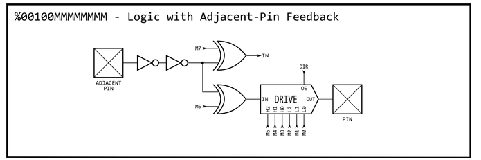
I am considering having a system with a low jitter external clock signal feeding the P2 and am hoping to regenerate this external clock to be output on another adjacent P2 pin and which can optionally be overridden by the P2 on demand and replaced with its own internal clock signal (it's actually an audio I2S application for an MCLK signal).
I was wondering if the mode shown above will keep the regenerated external clock signal's jitter under control or if it will introduce its own jitter in case the P2 is sampling it somewhere in this path with its own P2 clock (not shown). It looks like it's purely async logic in the diagram but I just don't know if the P2 will clock the signal somewhere and introduce more jitter.
Another way to do it is to just tri-state the external clock signal with another P2 control pin and external gate and then drive an internal clock out on a shared MCLK pin with the P2 directly, but I think the former approach is a little more flexible and lets me use the external clock and internal clock simultaneously/independently and it needs less hardware. There's also less chance of bus conflicts.
Comments
That needs clarified. Do you mean feeding into XIN pin of the Prop2?
EDIT: If you just mean a separate external clock input into the adjacent pin (PinB), and how the pin output (PinA) behaves ... In that listed mode, PinA will asynchronously follow PinB. The signal path is short and is unregistered, so not synchronised to the Prop2's internal clock. I would expect minimal added jitter. I have no experience though so can't put any numbers on it,
No, I want to just feed an external MCLK into a P2 IO pin and then output it regenerated (or overridden) on the adjacent pin to my external I2S DAC.
Update: Note this external clock would be sourced by one of these:
https://ww1.microchip.com/downloads/en/DeviceDoc/PL611-01.pdf
This was the first design iteration of the application but I want a programmable clock now so I can do 48kHz rates as well as 44.1kHz. Plus I plan some other goodies for the remaining pins...
You know the Prop2 ADCs are really good at audio. Far far better than at instrumentation. All that drift issue becomes irrelevant because it's primarily below 1 Hz.
Maybe so, though this particular board is intended as output only.
The precision of the DACs is damn good too. In hindsight, even better use of it could have been achieved if a duty dither smartpin mode was available to the DAC modes. It's amazing how much better duty (PDM) is over PWM. I guess PDM sits smack in the middle between PWM and PCM.
I'm sort of thinking of combining the two upper free IO pins as analog pins into the final output so this board can also do some analog output to the jack (capacitively mixed with the I2S DAC), but I might want to have the option of disabling this via DIP switches or something, as I think it'll probably mess with the output filter and could introduce unwanted noise and attenuate the signal. Still could be handy though.
If these optional analog pins are held tri-stated, I just wonder if it can still somehow pass in noise via the protection diodes from the supply rails to the output.
VIO would have to be quite noisy to inject clamping noise. I think you'd more likely pickup crosstalk from the I2S tracks.
Yeah it's probably worth a try at least to see how bad it is. May want to have a series resistor and series cap between the analog P2 pin and the existing junction at the 3.3uF and 10k load. What values to choose would be TBD, as is the best P2 DAC level to use in this analog case.
The other free pin would be for frequency selection between 48 and 44.1kHz. I plan to also dual purpose the other I2S outputs for jack detection purposes and optional SPDIF output as well as I found one of those combo 3.5mm jacks with internal LED for optical audio which will be good here.
P2 DACs are good enough to not even try any external DACs for audio. I want to try and use them as an external DACs for a RPi so I need a i2s code too to receive the audio signal.
The noise floor of these DACs, tested using an ear, an amplifier and an Eval board, is better than -100 dB.
The test signal I used was 3-bit "sine" wave and a 200 W amplifier at full volume, so I can hear this sine wave, its quantization noise and the analog noise floor.
Having >1 MHz sample rate at 16 bit resolution we can use a noise shaper, as in a P1, to convert 24-bit audio signal to 16-bit audio at 1.25 MHz (and get theoretical SNR at -140 dB and practical SNR at the analog output noise level).
ADCs are much more noisy. They are sufficient for everyday audio, but if you do the example from the Propeller Tool (ADC->DAC) you can hear the noise. For Hi-Fi audio input an external ADC board is needed. Maybe I can order this new Parallax made audio accessory board to test.
I don't know what algorithm makes the "noise" type DAC dithering, but I did the same test with a 3-bit sine wave using a "noise DAC" mode.
The 3-bit sine was much more distorted then with a much higher audible noise.
The most interesting experiment however was to try and output <1 Hz 3-bit sine wave. In this case the sine wave is not hearable and all you can hear is the DAC noise.
The noise was modulated, silent when 16-bit value was near the 8-bit level, loud when the 16-bit value was between 2 8-bit levels.
This means it is something like "duty noise", but but how it is generated inside a P2?
Very good. You've zero'd in on why PDM works better than PWM ... At mid PWM amplitude the drive is 50/50 sink/source at the modulation frequency so therefore has the greatest ripple. As it approaches 0% or 100% the short side of the pulse becomes very narrow so therefore only produces a tiny ripple.
With PDM, the pulse density becomes super fine oscillation at mid PDM amplitude so therefore resistive ripple is minimised. Frequency is highest at 50%. Much more likely to have inductive/capacitive switching ripple instead. And when approaching 0%/100% limits, the ripple doesn't change. This is because the smallest side of the pulse is always the same minimum time.
This noise modulation was hearable in the noise DAC mode, not PWM DAC mode. That's why I wonder what algorithm was used to generate that noise. There are algorithms that can generate a PDM/noise signal that has no frequencies in accoustic band, and that would make an "ideal" 8-to-16 bit extension, allowing any DAC period and still be silent.
Still, the P2 DACs with PWM extension is good enough to output a proper audio signal")
Oh, the smartpin's DAC random dither mode just takes a feed from the Xoroshiro128 hardware PRNG. It'll compare Y[7:0] against 8 bits of random data and dither accordingly. It's not the duty mode I was talking about.
Yes.
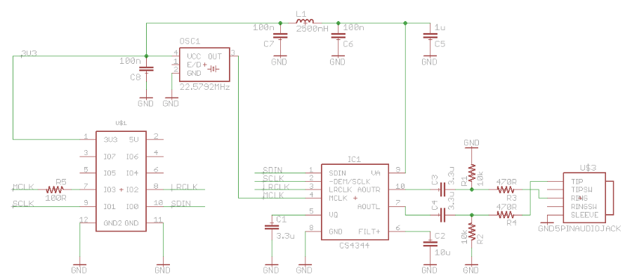
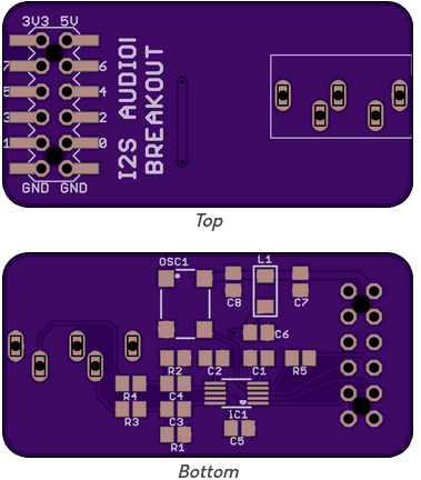
Got my design updated to include the new features. Just checking it all now. Some component values are subject to change. I hope the odd/even pins are symmetric when it comes to the pin mode shown at the top of the thread.
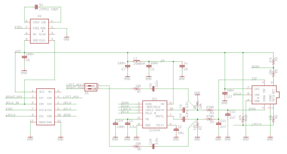
EDIT: last minute change was to flip LRCLK and SCLK pin mapping to the P2 (not shown in above schematic). This lets me use the external clock as a clock source for smartpin sync serial TX mode (just in case I find I need to). Also tweaked the top layer silk a bit more compared to the above.
EDIT2: updated layout and schematic above with new images. Fixed L&R pin mapping to be same as VGA A/V breakout
Wow, lots packed in there. I presume the optical feature is going to be usable. What sort of optical cable plugs into that socket?
Yeah it's tighter now. Could be shrunk a lot more (I've just spaced apart some 0805s to keep it simple to solder), and with shared values some of these parts could be resnets however for now it's easier to keep as individual resistors to test with different values if required.
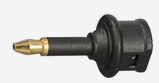
The jack is a combination optical OR electrical socket. You can plug in a normal 3.5mm phono line out cable or a S/PDIF cable into it - you can get a simple phono adapter for the typical square connector type plastic optical cables. Mac gear uses this approach for their optical capable ports.
This is an either/or setup so it shares a common pin for the LED output. The type of cable can be detected by the two DET pins on the connector. One pin goes low if anything is connected, the other pin additionally goes low if an electrical plug is connected - conducting via the common ground sleeve. It's quite a clever socket really.
I've tried to set it up so the detecting could also be dynamic, not just at start up. The SDIN pin sending I2S data could be quickly switched back to an input at the end of a bit or word and polled to sense a cable removal or being plugged in. The other LRCLK pin can also then be checked to determine the type of device. This way you could potentially spawn an S/PDIF COG on demand or switch back to regular I2S with mixed P2 output on the fly etc. That's the hope anyway.
Boards turned up today. The required parts arrived from Digikey today too. Now I just need to assemble it...seems a shame to ruin the pristine layer underside with my hand soldering, but I'll do my best. That DAC is not fun at 0.5mm pitch, lucky it's only 5 pins along each edge, and the SMD crystals are never much fun either. The passives are 0805's so not too bad there. Sort of think now perhaps I should have invested in a stencil and used my hotplate again.
Am very happy that the custom footprint I made for that optical connector fits correctly, as it was a rather weird shape with strange pin offsets.
EDIT:
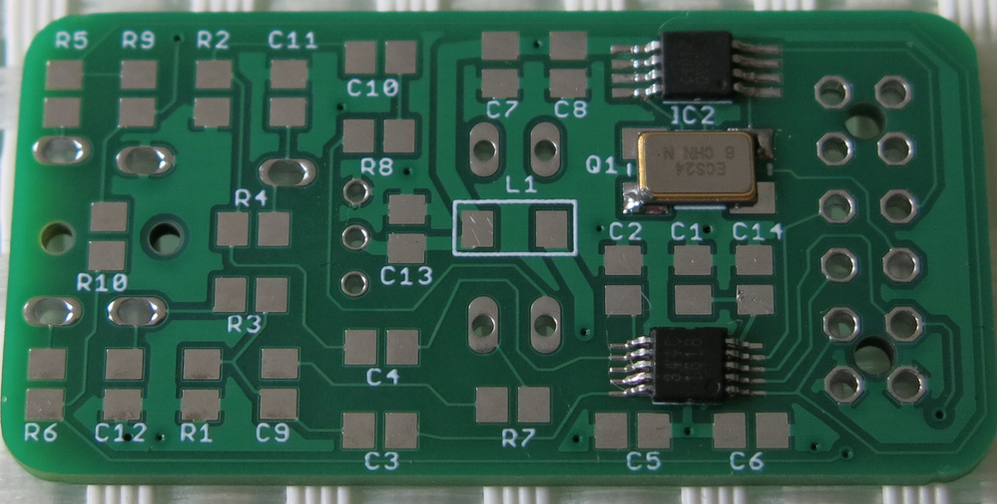
Ok soldering the harder SMDs weren't too bad in the end. I think that XTAL is down, but time will tell.
Job done, although looking at this enlarged pic now I might go around and reflow each passive another time with a larger chisel tip to clean up the joints a bit.
Update: The xtal & PLL clock synth is working. Seeing ~22.5MHz and ~24.5MHz clocks on scope as I toggle FSEL which is good. Now I need to port some I2S code... The S/PDIF LED also turns on when I pull SCLK high too.
Nice board!")
I have some I2S sound output working and now generating some interesting sound effects - it's not 100% bit synced yet. But it's outputting fairly cleanly on both channels.
Good thing is that the pin config mode I was asking about initially and am now using is working nicely.
CON _clkfreq = 256000000 BASE_PIN = 0 ' base pin of I2S breakout SDIN_PIN = BASE_PIN + 0 LRCLK_PIN = BASE_PIN + 1 SCLK_PIN = BASE_PIN + 2 FSEL_PIN = BASE_PIN + 3 MCLK_PIN = BASE_PIN + 4 MCLKIN_PIN = BASE_PIN + 5 PUB main() | sample, angle sample :=0 angle :=0 pinf(MCLKIN_PIN) wrpin(MCLKIN_PIN, 0) ' ensure no smart pin mode on MCLK IN pinl(FSEL_PIN) ' enable 44.1kHz MCLK input pinf(MCLK_PIN) ' setup MCLK pin wrpin(MCLK_PIN, P_LOGIC_B_FB) ' replicate MCLKIN to MCLK pinh(MCLK_PIN) pinf(SCLK_PIN) ' setup SCLK pin wrpin(SCLK_PIN, P_PLUS2_B | P_OE | P_SYNC_TX) ' MCLK is 2 pins above SCLK wxpin(SCLK_PIN, %1_01111) ' 16 MCLKs for each SCLK pinh(SCLK_PIN) wypin(SCLK_PIN, $ff00) ' SCLK output pattern pinf(LRCLK_PIN) ' setup LRCLK pin wrpin(LRCLK_PIN, P_PLUS1_B | P_OE | P_SYNC_TX) ' SCLK is 1 pin above LRCLK wxpin(LRCLK_PIN, %1_11111) ' 32 SCLKs for each LRCLK pinh(LRCLK_PIN) wypin(LRCLK_PIN, $ffff0000) ' LRCLK output pattern pinf(SDIN_PIN) ' setup SDIN pin wrpin(SDIN_PIN, P_PLUS2_B | P_OE | P_SYNC_TX) ' SCLK is 2 pins above SDIN wxpin(SDIN_PIN, %1_11111) ' 32 SCLKs for each stereo sample pinh(SDIN_PIN) repeat ' make the noise! waitus(22) ' a hack for now wypin(SDIN_PIN, (sample>>1) * $10001) ' it's not aligned, I know sample,_:=polxy($1000, angle) angle+=$3000Huh, readily available as a cable too it seems - https://www.pbtech.co.nz/product/CABAEN0000100/AEON-CT100-Optical-Cable-Toslink-Mini---Extra-Stre
Thanks. Yeah so far I think it has turned out reasonably well. Will have to finish the code and get some CD rips playing or something.
Even handier.
Fixed the bit sync/phase and found I had to reverse the sample to get it into correct bit order. Now it can generate a pure 1kHz tone and it sounds clean in headphone listening. Sample SPIN2 code attached. I found we can drop the P2 clock down to just above 2x the MCLK frequency for it to work, so any P2 frequency from 46MHz up will work for 44.1kHz, and 50MHz up for 48kHz.
This code could easily be made into an I2S object and it probably makes sense to have a couple of variants. A Cogless version where the SPIN2 code feeds it data at a fast enough rate when it is ready, and another with a driver Cog that optionally COGATNs a given group of COGs and reads audio sample data from a shared long in HUB. In fact in my view it's a bit of a waste of a COG when you can simple put the I2S instructions directly into your audio output COG and use it to sync to the sample rate. You just need to reverse the stereo sample bits with a REV and do a WYPIN writing the sample data and then wait until the data smartpin input goes high either by polling, waiting on an event or using an interrupt, so it's very minimal overhead after the smartpin setup is done. Plus you can still output analog/PWM/NCO samples in parallel on other pins too.
CON _clkfreq = 225_000000 ' just needs to be over 2x master clock rate BASE_PIN = 0 SDIN_PIN = BASE_PIN + 0 LRCLK_PIN = BASE_PIN + 1 SCLK_PIN = BASE_PIN + 2 FSEL_PIN = BASE_PIN + 3 MCLK_PIN = BASE_PIN + 4 MCLKIN_PIN = BASE_PIN + 5 LEVEL = $7fff ' maximum outut level ($7fff is full maximum) SINE_AMPLITUDE = LEVEL << 16 SQUARE = 0 ' non-zero for square wave output PUB main | sample, angle sample := 0 angle := 0 pinf(MCLKIN_PIN) ' clear out any prior smartpin config and keep MCLKIN as an input pin wrpin(MCLKIN_PIN, 0) pinl(FSEL_PIN) ' select 22.5792MHz clock in external PLL for 44.1kHz sample rate pinf(MCLK_PIN) ' clear out any prior smartpin config wrpin(MCLK_PIN, P_LOGIC_B_FB) ' setup logic with adjacent pin feedback (MCLK output = MCLKIN) pinh(MCLK_PIN) { ' optional internal clock generation pinf(MCLK_PIN) wrpin(MCLK_PIN, P_OE| P_NCO_FREQ) wxpin(MCLK_PIN, $00005) ' 225MHz/10 = 22.5MHz wypin(MCLK_PIN, $80000000) pinh(MCLK_PIN) } pinf(SCLK_PIN) ' clear out any prior smartpin config wrpin(SCLK_PIN, 0) pinh(SCLK_PIN) ' prepare SCLK logic high waitus(1) pinf(LRCLK_PIN) ' clear out any prior smartpin config wrpin(LRCLK_PIN, P_PLUS1_B | P_INVERT_B | P_OE | P_SYNC_TX) ' SCLK is 1 pin above LRCLK wxpin(LRCLK_PIN, %1_11111) ' 32 SCLKs for each LRCLK pinh(LRCLK_PIN) wypin(LRCLK_PIN, $ffff0000) ' LRCLK output pattern pinl(SCLK_PIN) ' toggle LRCLK output waitus(1) pinh(SCLK_PIN) ' LRCLK is advanced by one clock cycle to keep correct data phase relative to LRCLK waitus(1) pinf(SDIN_PIN) ' clear out any prior smartpin config wrpin(SDIN_PIN, P_PLUS2_B | P_INVERT_B | P_OE | P_SYNC_TX) ' SCLK is 2 pins above SDIN wxpin(SDIN_PIN, %0_11111) ' 32 SCLKs for each stereo sample pinh(SDIN_PIN) wypin(SDIN_PIN, 0) ' start with zeroed sample initially to avoid clicks/pops pinf(SCLK_PIN) wrpin(SCLK_PIN, P_PLUS2_B | P_OE | P_SYNC_TX) ' MCLK is 2 pins above SCLK wxpin(SCLK_PIN, %1_01111) ' 16 MCLKs for each SCLK pinh(SCLK_PIN) wypin(SCLK_PIN, $ff00) ' SCLK output pattern repeat ' make a tone wypin(SDIN_PIN, sample rev 31) ' send sample as serial output data (reversed) _, sample:=polxy(SINE_AMPLITUDE, angle) angle += muldiv64($ffffffff, 1000, 44100) '1kHz @44.1kHz sample rate (2^32*1000/44100 or thereabouts) sample &= $ffff0000 ' ignore LSBs if SQUARE ' convert to square wave if sample > 0 sample := SINE_AMPLITUDE else sample := -SINE_AMPLITUDE sample := sample + (sample >> 16) ' create a stereo sample (MSW=left, LSW=right) repeat until pinr(SDIN_PIN)The muldiv64() would be faster/smaller/exacter as a QFRAC 1000/44100 ... I see there is even an unsigned Spin FRAC operator.")
Intriguing that the CS4344 sample word format is big-endian bit order, like SPI. I had though I2S was rigidly spec'd only to be little-endian. I guess that is to suit interfacing with SPI controllers rather than the traditional PC97 southbridges.
Data says this
Selection Guide
The CS4344 family differs by Serial Audio format as follows:
• CS4344 — 16- to 24-bit, I²S
• CS4345 — 16- to 24-bit, Left-Justified
• CS4348 — 16-bit, Right-Justified
TI info shows his
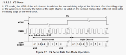
which indicates a 1 clock phase shift / delay, from WCLK edge to next data MSB
Yes I knew it could be off by one LSB bit with that MULDIV64. Probably should have just used some inline PASM but I was lazy at the time. I didn't see QFRAC in the list of builtins for v37. But FRAC is actually an operator as you mention. Maybe I wiil try out 1000 FRAC 44100.
Yeah I had to reverse it as I had it backwards initially. Made interesting sound effects but it was a pretty weird sound when fed with the sinusoidal data.
Currently looking at porting Scanlime's amazing P1 S/PDIF object, replacing the waitvid with a smartpin sync tx data transmission. I can't figure out a way the P2 can do it any faster than that. Brilliant code.
Yeah that was a problem until I figured out I could simply manually advance the LRCLK (WCLK) by one clock pulse data bit before I started the main SCLK clock input pin to feed both SDIN and LRCLK and then the one bit phase shift would remain after that. Thankfully the P2 automatically replicates the last serial output continuously on LRCLK so there is no slip after this one time setup.
Sorry, yeah, it was intended as a shorthand of the Cog's instruction QFRAC, not Spin. The dot,dot,dot was for me then looking up the Spin docs.
For I2S and perhaps other uses it would have been good if the P2's sync tx mode had a clock divisor option (like the async mode has a baud divisor). This would let you take a clock input and divide it down to get a clock to drive the serial output.
We already had this for async tx mode, so perhaps it could have potentially shared the hardware a little inside the smartpin to avoid lots of extra gates :