@rogloh - Good stuff. Do you need a P2D2? I still have to get new boards made yet but I still have plenty of the first lot.
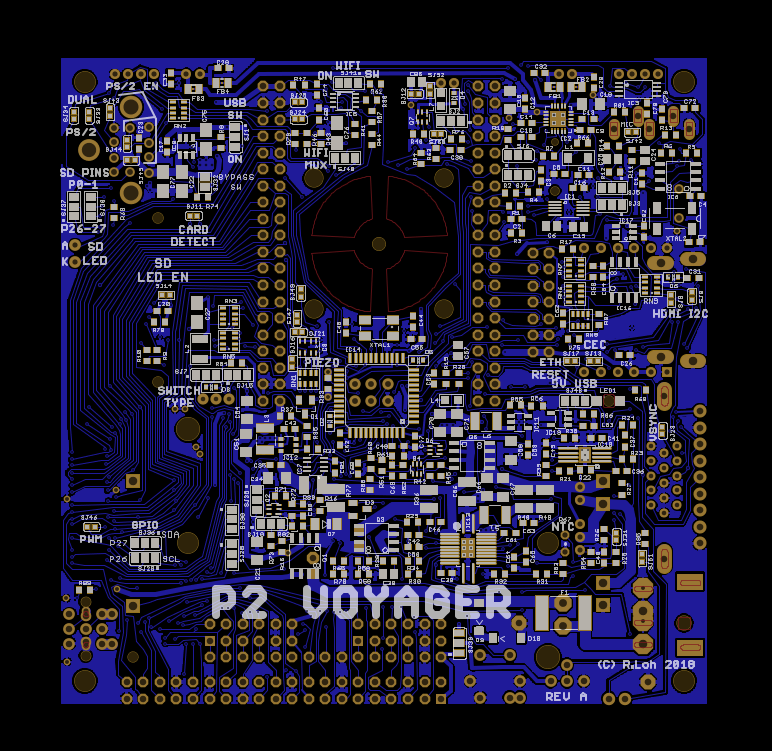
Which pcb software did you use? The reason I ask is because it looks like it is hand taped in some places where tracks almost touch and in others there is "rather poor" routing. Look at the attachment for an example.
@"Peter Jakacki", don't worry that is just an artifact of the gerber render tool and low res I used for the screen grab. It's much, much cleaner in real life and fully meets the 6 mil track and space contraints of the fab house.
I would love to get a real P2D2 soon. When do you think you might have the new one coming? If it's still a long while away maybe an older board makes sense. I am going to work with Tubular and Ozpropdev for the first board bringup once I validate the power supply aspects and they already have P2D2s, but the hope is that I might eventually get a new board too at some future time. Other parts hopefully arriving next week and I'll probably make it up early new year as Xmas delays things somewhat. I can send you a board to play with too.
I didn't mean the low res, that's expected but can you see what I mean. You see the router bending a track back around so that it has to squeeze two tracks between a pad rather than direct from one pad down between pads to the pad and vice-versa. But there are a ton of other questionable angles and spacing. Which router is that?
If I send off the artwork for the new board, even though it's that time of the year here, I think I should still get it in the next couple of weeks as I've done this before.
Well I guess the reason is that every track was hand routed so there are probably plenty of spacing discrepancies and where things were tight I shuffled things about bit by bit to meet constraints, plus the top layer adds its own routing complexities that are not shown. A future rev could certainly clean some of that up but I was tiring of tweaking all the tracks to get absolute alignment and perfect symmetry etc as component sizes got changed here and there so I sort of gave up on making it look perfect first go I guess. Apologies if required. It would become somewhat of a wasted effort if a respin is needed and I really want this to get done. It's a complex board to get right first go.
Yes Tubular in fact I think the part Peter identified from my board were the differential pair groups for HDMI and that part was actually routed this way as groups of two wires by the routing tool in order to try to control the impedance and match timing which is important on each pair, though there can be some small skew between pairs. That is actually true. But given I already have these wires going through a layer change twice first from the P2D2 board to mine and then via another connector to the other layer and over a few more (thankfully passive) tracks on another layer, all bets for impedance/timing are going to be off anyway. We'll see how well HDMI will work at ~250MHz for VGA - it only got added late mainly as a test for me so I could try to play with some bit bang TMDS signalling if I populated the connector. Will still give it a try though. Chip had his working with bare wires...
Circuit boards arrived today along with the stencil from PCB fab house. Pretty happy so far with the overall quality and drill hole alignment and silkscreen readability and it seems to be made as ordered. Tried a few components for fitment and spacing looks good, despite being packed in. So long as P2D2 doesn't grow larger on its bottom edge with the power regs I think I should be okay. So please Peter, don't increase it any further or I'm basically screwed. :frown:
I found a minor issue with the VGA connector being very tight to install in place and I'll need to open up the holes a fraction with a PCB drill to help. Weird as I've used this particular footprint and component before in another project and it fit, could be just variation in supplied parts. Will increase hole size from 0.7mm to 0.8mm on next spin in any case. Stencil alignment looks okay too when I held it over the board.
Posted some pics of this board etc and within the instrument enclosure.
Roger, some parts from different manufacturers sometimes have slightly different hole size requirements. I've seen this particularly for VGA connectors.
Yes Cluso, the pin diameter was meant to be from 0.6 to 0.63mm but the connector I'd obtained probably measures more like 0.73mm or so with my calipers and the pins are not actually very round either. I can open up the hole on the board a bit manually for these test boards with a small drill, or maybe search for a different VGA connector with smaller pins, but there is some variance in depth from the facing edge to the 3 rows of pins as well. These DE15 connectors are not exactly standardized but it should be easy to sort out one way or another.
Yes, there are quite a few VGA variants.
What dimensions do you need and I'll see if I have any.
Thanks Cluso but I was already able to drill out to 0.8mm from 0.7mm using a Dremel, press and a PCB drill bit. Connector fits snugly now. Good thing is that only one connection actually passes up to non-solder side and it was not affected by reducing its plated hole thickness by drilling. The rest of the connections already remain on the solder side so it wouldn't even matter for those if any of the inner plating was lost. Looks clean.
Last parts I was waiting for (excepting the actual P2D2) finally arrived for this project after 3 weeks of delays due to hols and some capacitor shortages. OMG where do I begin! Around 100 line items to check here and sort.
Will just start out with building and testing the power supply regulator circuits as a standalone test board I guess, then proceed from there...
Spent a couple of hours today sorting through all those parts and put the passives, connectors, diodes and FETs into some handy plastic tray boxes with labels so I can locate them faster compared to all those plastic bags they came in. Keeping the other moisture and static sensitive stuff safely in their foil bags for now until its time to solder them.
Now ready to build the 5V buck regulator section on the first test board and take it from there.
@idbruce, yes it is - especially when you've been waiting for a while for them.
This afternoon I was also able to solder up the main 5V step down regulator and input reverse FET protection stuff. Certainly not my best work as 0603 is getting somewhat small for me to see without proper magnification etc, but it should hopefully now be sufficient to test the circuit with any luck.
This morning, I will be making my first attempt at a surface mount component
I will be attempting to surface mount a 20 pin SSOP. A MCP23008 to be exact. I can only imagine the joy
Take your time. 0.65mm pitch is usually reasonably doable with some care, plenty of flux and desolder wick if you mess it up. I have one of those package types on my board too but in the 24 pin size for HDMI. At least its pins protrude out beyond the package unlike QFN/DFN or BGA etc. I only have one QFN device on my board, and it worries me. A couple of other 0.5mm parts are not going to be enjoyable either.
Much easier if you use a flux pen on the pcb and under the pins on a QFP/QFN first. Also very fine solder with internal rosin. Leaded solder is easier for inexperienced users.

 rogloh
Posts: 6,412
rogloh
Posts: 6,412

Comments
Which pcb software did you use? The reason I ask is because it looks like it is hand taped in some places where tracks almost touch and in others there is "rather poor" routing. Look at the attachment for an example.
Thanks Ym2413a, there will definitely be plenty to test and then play with using my motherboard once it all works.
I would love to get a real P2D2 soon. When do you think you might have the new one coming? If it's still a long while away maybe an older board makes sense. I am going to work with Tubular and Ozpropdev for the first board bringup once I validate the power supply aspects and they already have P2D2s, but the hope is that I might eventually get a new board too at some future time. Other parts hopefully arriving next week and I'll probably make it up early new year as Xmas delays things somewhat. I can send you a board to play with too.
If I send off the artwork for the new board, even though it's that time of the year here, I think I should still get it in the next couple of weeks as I've done this before.
You can always claim the track routing is deliberate, to even up the timing
I found a minor issue with the VGA connector being very tight to install in place and I'll need to open up the holes a fraction with a PCB drill to help. Weird as I've used this particular footprint and component before in another project and it fit, could be just variation in supplied parts. Will increase hole size from 0.7mm to 0.8mm on next spin in any case. Stencil alignment looks okay too when I held it over the board.
Posted some pics of this board etc and within the instrument enclosure.
What dimensions do you need and I'll see if I have any.
Thanks Cluso but I was already able to drill out to 0.8mm from 0.7mm using a Dremel, press and a PCB drill bit. Connector fits snugly now. Good thing is that only one connection actually passes up to non-solder side and it was not affected by reducing its plated hole thickness by drilling. The rest of the connections already remain on the solder side so it wouldn't even matter for those if any of the inner plating was lost. Looks clean.
Will just start out with building and testing the power supply regulator circuits as a standalone test board I guess, then proceed from there...
Now ready to build the 5V buck regulator section on the first test board and take it from there.
This afternoon I was also able to solder up the main 5V step down regulator and input reverse FET protection stuff. Certainly not my best work as 0603 is getting somewhat small for me to see without proper magnification etc, but it should hopefully now be sufficient to test the circuit with any luck.
Going back to something you said earlier...
This morning, I will be making my first attempt at a surface mount component
I will be attempting to surface mount a 20 pin SSOP. A MCP23008 to be exact. I can only imagine the joy
Is that little 6 pin the small package (SOT-363?) ?
LOL... I can only imagine his joy with that one
Take your time. 0.65mm pitch is usually reasonably doable with some care, plenty of flux and desolder wick if you mess it up. I have one of those package types on my board too but in the 24 pin size for HDMI. At least its pins protrude out beyond the package unlike QFN/DFN or BGA etc. I only have one QFN device on my board, and it worries me. A couple of other 0.5mm parts are not going to be enjoyable either.
Yes unfortunately - and I DESPISE those! Took me forever to get it right on a prior board.
I can only imagine my joy if my first surface mount was a QFN
However, your same advice applies: