How would you mount a fan, if needed? Would having at least a couple of 2mm holes make sense? Even if too big for the 3mm thick fan, it'd allow some kind of adapter plate. There are also a smaller series of solnet nuts from Pemnet, to suit M1.6 screws and similar. Diameter is around 3.7 or 3.8mm from memory
How would you mount a fan, if needed? Would having at least a couple of 2mm holes make sense? Even if too big for the 3mm thick fan, it'd allow some kind of adapter plate. There are also a smaller series of solnet nuts from Pemnet, to suit M1.6 screws and similar. Diameter is around 3.7 or 3.8mm from memory
Yeah I was planning to add some mounting holes either for a fan itself over the P2 if possible or for a bracket/PCB plate that holds a fan over the P2. I still think we'd potentially want one given the tiny volume of the enclosure, just to stir the air around and try to exhaust some of the heat. The heat building up has got to go somewhere when spread over the PCB so it's prudent to make a design that allows for a tiny fan. Plus it makes no noise and draws little current so why not include the option of having one if there's room for it. I'll also include some pads for the fan's power wires at both 3.3V and 5V since we've identified fans that run at both these voltages. I wonder if a fan would add much electrical noise to a 3.3V rail...? Maybe a LDO is needed? I was also considering a separate LDO for the PSRAMs on the other side of the board but it's probably not needed. If I have room for a footprint I may include it with some jumper option of using it instead of the main switcher.
The new FireAnt P2 PCB is starting to come together and I now know it can all fit. It's not yet complete and I still to need do quite a few things like complete the remaining PSRAM routing and do a major trace tidy up, add some fan mounting holes and power, the in pad vias for the P2 ground, etc. Am debating 4 vs 6 layers. I have two of the current 4 layers already available as grounds/thermal and have tried to avoid a whole wall of vias to avoid blocking too much sideways heat transfer, by trying to group and stagger them where possible (see pic of one of the layers). I can probably get the PSRAM closer too. I may still add 2 more layers to help with heat.
Also decided on using two separate 3.3V LDOs instead of the high current switching reg on Lachlan's version, one will be just used for PSRAMs & OSC on the right side and the other is for uSD/Flash/GPi IO on top/left/bottom. Neither should draw all that much current, eg. flash only at boot, uSD only at start of game load, video IO switching only at 25MHz. The FTDI chip if fitted is USB bus powered too.
@rogloh said:
Neither should draw all that much current, eg. flash only at boot, uSD only at start of game load, video IO switching only at 25MHz. The FTDI chip if fitted is USB bus powered too.
Don't count on the SD card not coming on under load, MegaYume and MisoYume can back up cartridge NVRAM in the background. And of course native games like SpinHexagon will do audio streaming.
Good to know. The small LDO can do 500mA so I suspect that 25MHz IO + SD current should be less than this. I also have a large 1206 sized cap on the SD supply acting as a reservoir to help with instantaneous write current bursts/spikes.
How would you mount a fan, if needed? Would having at least a couple of 2mm holes make sense? Even if too big for the 3mm thick fan, it'd allow some kind of adapter plate. There are also a smaller series of solnet nuts from Pemnet, to suit M1.6 screws and similar. Diameter is around 3.7 or 3.8mm from memory
Not quite there yet @Tubular but I think with some more shuffling and compression of part spacing I might be able to get the original solder nut size to fit the board. It won't be quite centralized like before but we might be able to modify your fan board or make another variant that accommodates the different hole offsets from the centerline. I still need to move the PSRAMs in closer too. I hope the countersunk M2's screws can fit in, there won't be a large amount of space so it's best to make this fan board a rather thin 0.8mm PCB.
I also wonder if we couldn't use simple header pins to hold it, and they could transfer the fan power too. I almost want to glue the fan within a PCB square hole cutout to gain another 0.8mm. We've only got 6mm total clearance above the board to the plastic cartridge inside surface and this doesn't include the P2 height, plus we want a small gap for air to actually flow over the P2. If the fan was mounted inside a cutout instead of screwed to the PCB plate it might give us about 1mm of gap for that (6mm-1.2mm-3.8mm = 1mm). We could shim it while gluing to provide just the right clearance. We could also drill a few holes in the cartridge above the fan and/or along the top edge for more airflow if (most probably) required. Routing out some of the inner surface of the plastic might gain us a tad more clearance if needed. Calipers measured about 1.4mm thick plastic there.
Make the back side GND, behind the Prop2, as gold flashed copper. Then a shaped heat-sink can be neatly pressed onto it for good heat-sinking. And those screw mounts could also be exposed right through to make the heat-sink be a ridged mount too. Have the back of the cartridge be aluminium. Can even give it ribs. Then a fan shouldn't be needed.
Oh, oops, I see the FireAnt components are actually facing outward toward the back of the handheld ... What's the chances of flipping the components to the other side so then the heat sink side is facing outward?
@evanh said:
Oh, oops, I see the FireAnt components are actually facing outward toward the back of the handheld ... What's the chances of flipping the components to the other side so then the heat sink side is facing outward?
At this stage, very hard. A gap for the P2 and everything else would need to be routed out on the back and the board layout would have to be redesigned. 16 of the edge connector signals would have to cross the whole board from the top to the bottom making routing painful - although maybe with 6 layers not quite so hard. The PSRAMs really need to be where they are on the board, to not interfere with the SD card reader. And a two sided load on a hotplate at home, not really practical. Real PITA stuff to do. I think I need to keep the P2 upper surface on top as I have and I don't mind the fan if it works and stops this thing heating up to over 77C when enclosed. It doesn't make any audible noise.
One thing I could consider though is a thin metal plate under the board which attaches to those solder nuts which might carry heat from below up through those nuts to the top board perhaps. I'd still have to route out the plastic to make room for it though.
For reference here is the bottom of the cartridge that the FireAnt board sits over (bottom layer contacts it). You can see there is a small lowered section of it where a flat flex cable ran to the RasPi USB port. I could route out the rest of it, perhaps. Seems like you could gain about 1mm without sacrificing too much plastic strength.
If I could make a 3d model of it it could be remade in Aluminium but that's getting too involved.
@evanh you can see here how most of the signals are currently routed (still a WIP) - if the P2 is flipped to the bottom layer by spinning it around 180 degrees horizontally it's difficult to get the PSRAM signals where I want them on the right side. If it's flipped vertically, then many the signals have to cross from top to bottom. The parallel RGBS pins also needs 32 contiguous IO (of which I steal some unused bits for misc signals). Plus there is still the issue of getting all the components to fit by clearing all the plastic under the board - it'd be nicer to lift the board up a bit to fit it in but the edge fingers won't contact then. They need to sit in the plane they are currently in (and kept to a 0.8mm board). We attempted other PCB thicknesses and found it wouldn't fit nicely. Also the USB-C and microSD still need to be on the top surface - not sure how I'd solder them separately. We have enough additional mechanical constraints to consider here.
@evanh said:
Way too small for me though. I was brought up using TV sets and chunky joysticks.
Yeah I know, but it's also useful as a portable device. I also want to make that external converter box I can hook to a TV and send VGA converted to HDMI (via a 3m long USB-C cable). Then you can sit back and play on a TV tethered using the handheld as a controller.
Just read that the APS6404 PSRAM recommended low ESR 1uF bypass caps and IIRC I only fitted 0.1uF caps. So I should really desolder those 4 and try it with larger caps, maybe that will help the higher frequency performance a bit.
Also I've completed the net routing on the Rev 2 all in one FireAnt board that contains the P2 as well - just have to do a fan power connection with its own current path to avoid noise and add the in pad P2 vias and it should be done. I'll have to decide pretty soon if I want 4 vs 6 layers. Only two of my layers are mostly ground and will transfer heat but I could add two new copper layers below the top red SMD layer closest to the heat source for a 2x price increase in the PCBs. It'll still get rather hot in the case though I'm sure. Also this time the PSRAM routing is much tighter and very close to MXX's design so hopefully should reach decent speeds as well.
from my experience when I moved from a 4 layers board to a 6 layers board I noticed a major improvement in heat dissipation (aboout 10°C lower on P2 with 6 layers) due to less insulation material between layers.
In addition, I don't see any via under the P2, these are needed for heat transfer through all layers, like in my previous pictures.
Last thing, I would extend heat disspation inner layers to the edges of the board (also under the connector), everything matters!
Just read that the APS6404 PSRAM recommended low ESR 1uF bypass caps and IIRC I only fitted 0.1uF caps. So I should really desolder those 4 and try it with larger caps, maybe that will help the higher frequency performance a bit.
from my experience when I moved from a 4 layers board to a 6 layers board I noticed a major improvement in heat dissipation (aboout 10°C lower on P2 with 6 layers) due to less insulation material between layers.
Yeah I think I'll go with 6 also.
In addition, I don't see any via under the P2, these are needed for heat transfer through all layers, like in my previous pictures.
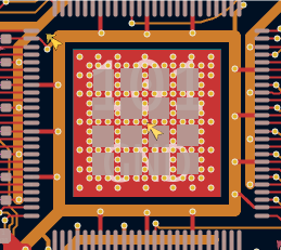
Yeah I'd mentioned I still had to do that and I've done it since. Here's what I've got now - uses same pattern as yours I think with a 15x15 matrix.
Last thing, I would extend heat disspation inner layers to the edges of the board (also under the connector), everything matters!
Definitely. I have the metal SD connector and USB-C connector which can assist too.
Just read that the APS6404 PSRAM recommended low ESR 1uF bypass caps and IIRC I only fitted 0.1uF caps. So I should really desolder those 4 and try it with larger caps, maybe that will help the higher frequency performance a bit.
I used 2.5 uF 0402 case.
Yeah I need to lookup what I may have ordered for these 0.1uF bypass caps for the first board version we made, but I think I've probably placed some older 0603 ones I just had left over from prior projects and I'm not sure what the temp rating was for those. The 1uF ones I can get fast locally for testing this are unfortunately only Y5Vs and can drop up to 82% at higher temp, which my board can certainly suffer from. So I'll probably need to wait for the next Mouser/Digikey order and I'll be sure to select better grade caps for these parts in the next board.
Yeah I've used 0.3mm drill holes which are pretty small, but left gaps in the pattern for the solder paste to not wick through too badly through these. I once heard that it can cause gas bubbles to explode or something if the paste gets into the holes. It's probably about 75% of the 225 holes that go through to the layers below. Gets pricier for using tiny drill holes below 0.3mm, board cost doubles again as it then includes a Kelvin test as well.
As part of the last PCB order, and to try to assist with potential thermal issues I also included a small 1mm thick fan board that sits above the FireAnt and can contain a 15x15mm fan in a cutout. 5V power get supplied through the solder nuts with series resistors on the FireAnt's PCB to these terminals to drop the voltage to 3V if needed and also protect against direct shorts. I drilled some holes for some more airflow above the PSRAMs which are otherwise covered by this board. So this is not intended as a heatsink just a mounting bracket designed to help circulate the hot air inside the case and blow over the P2 to cool it more. We'll see how well it all goes on the rev 2 board with 6 layers. I threw a cap in parallel with the fan wires to try to reduce noise spikes. Maybe I've created one nice inductive loop or something from this circuit, LOL. It's only 30mA though.
LOL, it's actually a nice cool product, but the power draw's a bit high in this case. Have to carry around a separate 2A supply perhaps.
It'd be interesting to try this for projects where lots of power is available and heat is the primary concern as it's a good fit for the P2's physical size.
@Wuerfel_21 does your PSRAM require the RBX (row boundary crossing) PSRAMs to work? My memory driver fragments transfer requests at row boundaries so probably doesn't need the RBX version, does your code do the same or do you cross row boundaries in the same transfer? I ask because we may have just ordered this cheaper type of PSRAM for the FireAnt project by mistake. It's the difference between 3SQR vs 3SQN suffix on the APS6404L chips. It looks like the P2-Edge rev B uses the 3SQR type which is row boundary crossing enabled (albeit rated at lower speed when crossing which probably makes it less reliable at high transfer speeds anyway). I also need to check what I have on my various boards, although I think some it might even be unlabelled "IOT RAM" from Adafruit with the labels intentionally removed. Why??? - seems very dodgy.
@Tubular said:
The good news is that we now have both 3SQR and 3SQN types coming. Merry ChrisPsramas...
Cool. So crisis averted. Thanks. In any case it might be moot if the emulator code from Wuerfel doesn't cross row boundaries. Both types of PSRAM would likely be workable. I remember back ages ago when first writing drivers for this memory that data problems could happen if you cross the boundary - so I was (likely) either using the original SQN version or running it too fast when crossing.
I ostensibly respect row boundaries, but I recall a case where the code for that was faulty and it worked anyways, so idk if it's fully correct. I wonder if the two part variations are just different bins of the same thing... It's also very strange that RBX is only rated for a lower speed.
The sprite and ADPCM transfers in NeoYume have no row boundary check, because they always read aligned blocks of 8/16 bytes, so no row boundary can be crossed. Clever.
Relatedly, for my 3D engine, writing custom PSRAM code is coming up... (after finally fixing ALL[citation needed] clipping bugs) I'm thinking better performance + lower complexity can be achieved if each framebuffer scanline (320px 16bpp = 640 bytes) was aligned such that it doesn't cross a row boundary. For 1K pages (PSRAM4), this would create a lot of padding, but for 2K pages (PSRAM8) or larger, 3 lines can be packed into a page with a nice 128 bytes of padding (convenient size for re-use e.g. as audio buffer). So wondering if I should just omit PSRAM4 support in there... Any die-hard PSRAM4 fans out there?
Thanks, @Wuerfel_21 . Sounds good then. We'll probably try to install the "better" RBX version just in case and it'll be compatible with the P2 Edge's choice.
Aligning to row boundaries always improves performance if the larger burst reads/writes can be done in a single atomic transfer within the row and don't get fragmented. If you can keep PSRAM4 support even if at lower performance it would be nice, rather than simply preclude it. PSRAM4 is still good for a single wide breakout, plus I have a couple of useful boards with just the 4 bit setups (my P2 Tablet, and a retro computer platform for the Z80 but could be a general purpose P2 system as well).
The rev 2 FireAnt P2 PCBs arrived back this morning. They turned out pretty nice and also fit inside the cartridge a little better now with some custom size tweaks I added after doing rev 1.
The gold square in the middle of the P2 is still connected through to the other layers. They've actually filled the vias so it looks solid but when I examined in close up I could see the array pattern of thermal via holes 15x15 (~75% used). I probably could have used the entire hole array since the paste can't even get through it now. The PCB manufacturer only does through hole vias so the back of the board makes it looks a little like it has caught chicken pox with the ground plane clearance of all the other non-grounded via signals on the board, lol.
Before I sent it off I also decided to remove all the component designators which will make manual assembly slightly more challenging for me but makes for a cleaner final board. The CC1/CC2 pins of the USB-C connector can be used for connecting the standard 5.1k pulldowns or can be optionally fed a composite sync for my external USB-C to VGA/HDMI PCB (which also arrived today and is shown too inside its selected enclosure). That board has had a LMH1980 sync separator circuit added to the path for VGA hsync and vsync signals (although it is yet untested), the remaining part is simply the micro USB power and PC data port, the USB-C connection to the FireAnt board and a copy of what I'd already used in the P2 VGA to HDMI breakout board originally discussed here: https://forums.parallax.com/discussion/177903/converting-component-vga-audio-to-hdmi-on-p2 The VGA video signal is now also buffered with a 3 input video amp (THS7316) before driving the VGA port so it can also be 75 ohm terminated by the MS9288A chip at the same time for output via HDMI.
All needed parts for this arrived yesterday and today so I'm now set to build this rev 2 board. As Christmas is rapidly advancing it's now getting very busy here so I may not have a lot of time to work on this before the actual break but I am eager to make it up whenever I can. The (optional?) little fan board is also shown here along with the tiny 3mm tall fan I'd ordered. I quickly tried it at 3.3V and it gives pretty decent airflow, seemingly more than that other 5V fan I tried before. It was slightly audible when touching the surface due to vibration but not really noticable with an air gap. Once it's all inside the enclosure I don't think it will be audible at all. We'll see...


Comments
Looks good roger.
How would you mount a fan, if needed? Would having at least a couple of 2mm holes make sense? Even if too big for the 3mm thick fan, it'd allow some kind of adapter plate. There are also a smaller series of solnet nuts from Pemnet, to suit M1.6 screws and similar. Diameter is around 3.7 or 3.8mm from memory
Yeah I was planning to add some mounting holes either for a fan itself over the P2 if possible or for a bracket/PCB plate that holds a fan over the P2. I still think we'd potentially want one given the tiny volume of the enclosure, just to stir the air around and try to exhaust some of the heat. The heat building up has got to go somewhere when spread over the PCB so it's prudent to make a design that allows for a tiny fan. Plus it makes no noise and draws little current so why not include the option of having one if there's room for it. I'll also include some pads for the fan's power wires at both 3.3V and 5V since we've identified fans that run at both these voltages. I wonder if a fan would add much electrical noise to a 3.3V rail...? Maybe a LDO is needed? I was also considering a separate LDO for the PSRAMs on the other side of the board but it's probably not needed. If I have room for a footprint I may include it with some jumper option of using it instead of the main switcher.
The new FireAnt P2 PCB is starting to come together and I now know it can all fit. It's not yet complete and I still to need do quite a few things like complete the remaining PSRAM routing and do a major trace tidy up, add some fan mounting holes and power, the in pad vias for the P2 ground, etc. Am debating 4 vs 6 layers. I have two of the current 4 layers already available as grounds/thermal and have tried to avoid a whole wall of vias to avoid blocking too much sideways heat transfer, by trying to group and stagger them where possible (see pic of one of the layers). I can probably get the PSRAM closer too. I may still add 2 more layers to help with heat.
Also decided on using two separate 3.3V LDOs instead of the high current switching reg on Lachlan's version, one will be just used for PSRAMs & OSC on the right side and the other is for uSD/Flash/GPi IO on top/left/bottom. Neither should draw all that much current, eg. flash only at boot, uSD only at start of game load, video IO switching only at 25MHz. The FTDI chip if fitted is USB bus powered too.
Don't count on the SD card not coming on under load, MegaYume and MisoYume can back up cartridge NVRAM in the background. And of course native games like SpinHexagon will do audio streaming.
Good to know. The small LDO can do 500mA so I suspect that 25MHz IO + SD current should be less than this. I also have a large 1206 sized cap on the SD supply acting as a reservoir to help with instantaneous write current bursts/spikes.
Not quite there yet @Tubular but I think with some more shuffling and compression of part spacing I might be able to get the original solder nut size to fit the board. It won't be quite centralized like before but we might be able to modify your fan board or make another variant that accommodates the different hole offsets from the centerline. I still need to move the PSRAMs in closer too. I hope the countersunk M2's screws can fit in, there won't be a large amount of space so it's best to make this fan board a rather thin 0.8mm PCB.
I also wonder if we couldn't use simple header pins to hold it, and they could transfer the fan power too. I almost want to glue the fan within a PCB square hole cutout to gain another 0.8mm. We've only got 6mm total clearance above the board to the plastic cartridge inside surface and this doesn't include the P2 height, plus we want a small gap for air to actually flow over the P2. If the fan was mounted inside a cutout instead of screwed to the PCB plate it might give us about 1mm of gap for that (6mm-1.2mm-3.8mm = 1mm). We could shim it while gluing to provide just the right clearance. We could also drill a few holes in the cartridge above the fan and/or along the top edge for more airflow if (most probably) required. Routing out some of the inner surface of the plastic might gain us a tad more clearance if needed. Calipers measured about 1.4mm thick plastic there.
Make the back side GND, behind the Prop2, as gold flashed copper. Then a shaped heat-sink can be neatly pressed onto it for good heat-sinking. And those screw mounts could also be exposed right through to make the heat-sink be a ridged mount too. Have the back of the cartridge be aluminium. Can even give it ribs. Then a fan shouldn't be needed.
Oh, oops, I see the FireAnt components are actually facing outward toward the back of the handheld ... What's the chances of flipping the components to the other side so then the heat sink side is facing outward?
Or flip just the tight in low profile components of the Prop2 and capacitors. That way the heat-sink can be located where the fan would be.
At this stage, very hard. A gap for the P2 and everything else would need to be routed out on the back and the board layout would have to be redesigned. 16 of the edge connector signals would have to cross the whole board from the top to the bottom making routing painful - although maybe with 6 layers not quite so hard. The PSRAMs really need to be where they are on the board, to not interfere with the SD card reader. And a two sided load on a hotplate at home, not really practical. Real PITA stuff to do. I think I need to keep the P2 upper surface on top as I have and I don't mind the fan if it works and stops this thing heating up to over 77C when enclosed. It doesn't make any audible noise.
One thing I could consider though is a thin metal plate under the board which attaches to those solder nuts which might carry heat from below up through those nuts to the top board perhaps. I'd still have to route out the plastic to make room for it though.
For reference here is the bottom of the cartridge that the FireAnt board sits over (bottom layer contacts it). You can see there is a small lowered section of it where a flat flex cable ran to the RasPi USB port. I could route out the rest of it, perhaps. Seems like you could gain about 1mm without sacrificing too much plastic strength.
If I could make a 3d model of it it could be remade in Aluminium but that's getting too involved.
@evanh you can see here how most of the signals are currently routed (still a WIP) - if the P2 is flipped to the bottom layer by spinning it around 180 degrees horizontally it's difficult to get the PSRAM signals where I want them on the right side. If it's flipped vertically, then many the signals have to cross from top to bottom. The parallel RGBS pins also needs 32 contiguous IO (of which I steal some unused bits for misc signals). Plus there is still the issue of getting all the components to fit by clearing all the plastic under the board - it'd be nicer to lift the board up a bit to fit it in but the edge fingers won't contact then. They need to sit in the plane they are currently in (and kept to a 0.8mm board). We attempted other PCB thicknesses and found it wouldn't fit nicely. Also the USB-C and microSD still need to be on the top surface - not sure how I'd solder them separately. We have enough additional mechanical constraints to consider here.
Yeah, would be a big job to make everything fit. Thanks for thinking about it.
I only just now took a look back to find all the early photos of where everything sits. Found the YT video link and watched it. The RPi makes for an impressive emulator itself. - https://forums.parallax.com/discussion/comment/1568626/#Comment_1568626
Way too small for me though. I was brought up using TV sets and chunky joysticks.
Yeah I know, but it's also useful as a portable device. I also want to make that external converter box I can hook to a TV and send VGA converted to HDMI (via a 3m long USB-C cable). Then you can sit back and play on a TV tethered using the handheld as a controller.
Just read that the APS6404 PSRAM recommended low ESR 1uF bypass caps and IIRC I only fitted 0.1uF caps. So I should really desolder those 4 and try it with larger caps, maybe that will help the higher frequency performance a bit.
Also I've completed the net routing on the Rev 2 all in one FireAnt board that contains the P2 as well - just have to do a fan power connection with its own current path to avoid noise and add the in pad P2 vias and it should be done. I'll have to decide pretty soon if I want 4 vs 6 layers. Only two of my layers are mostly ground and will transfer heat but I could add two new copper layers below the top red SMD layer closest to the heat source for a 2x price increase in the PCBs. It'll still get rather hot in the case though I'm sure. Also this time the PSRAM routing is much tighter and very close to MXX's design so hopefully should reach decent speeds as well.
Great work @rogloh!
from my experience when I moved from a 4 layers board to a 6 layers board I noticed a major improvement in heat dissipation (aboout 10°C lower on P2 with 6 layers) due to less insulation material between layers.
In addition, I don't see any via under the P2, these are needed for heat transfer through all layers, like in my previous pictures.
Last thing, I would extend heat disspation inner layers to the edges of the board (also under the connector), everything matters!
I used 2.5 uF 0402 case.
Thanks.
Yeah I think I'll go with 6 also.
Yeah I'd mentioned I still had to do that and I've done it since. Here's what I've got now - uses same pattern as yours I think with a 15x15 matrix.
Definitely. I have the metal SD connector and USB-C connector which can assist too.
Yeah I need to lookup what I may have ordered for these 0.1uF bypass caps for the first board version we made, but I think I've probably placed some older 0603 ones I just had left over from prior projects and I'm not sure what the temp rating was for those. The 1uF ones I can get fast locally for testing this are unfortunately only Y5Vs and can drop up to 82% at higher temp, which my board can certainly suffer from. So I'll probably need to wait for the next Mouser/Digikey order and I'll be sure to select better grade caps for these parts in the next board.
@cgracey showed us a layout he is working on. Had a gazzillion vias under P2.
Maybe it was 15x15 array of 0.3 mm vias
Yeah I've used 0.3mm drill holes which are pretty small, but left gaps in the pattern for the solder paste to not wick through too badly through these. I once heard that it can cause gas bubbles to explode or something if the paste gets into the holes. It's probably about 75% of the 225 holes that go through to the layers below. Gets pricier for using tiny drill holes below 0.3mm, board cost doubles again as it then includes a Kelvin test as well.
New rev2 6 layer boards are ordered! I also picked up some better SMD bypass caps for the PSRAMs to try on the rev 1 when I can - thanks Tubular.
As part of the last PCB order, and to try to assist with potential thermal issues I also included a small 1mm thick fan board that sits above the FireAnt and can contain a 15x15mm fan in a cutout. 5V power get supplied through the solder nuts with series resistors on the FireAnt's PCB to these terminals to drop the voltage to 3V if needed and also protect against direct shorts. I drilled some holes for some more airflow above the PSRAMs which are otherwise covered by this board. So this is not intended as a heatsink just a mounting bracket designed to help circulate the hot air inside the case and blow over the P2 to cool it more. We'll see how well it all goes on the rev 2 board with 6 layers. I threw a cap in parallel with the fan wires to try to reduce noise spikes. Maybe I've created one nice inductive loop or something from this circuit, LOL. It's only 30mA though.
Wonder if one of these peltier coolers would work:
https://www.digikey.com/en/products/detail/same-sky-formerly-cui-devices/CP60233/1747365
LOL, it's actually a nice cool product, but the power draw's a bit high in this case. Have to carry around a separate 2A supply perhaps.
It'd be interesting to try this for projects where lots of power is available and heat is the primary concern as it's a good fit for the P2's physical size.
@Wuerfel_21 does your PSRAM require the RBX (row boundary crossing) PSRAMs to work? My memory driver fragments transfer requests at row boundaries so probably doesn't need the RBX version, does your code do the same or do you cross row boundaries in the same transfer? I ask because we may have just ordered this cheaper type of PSRAM for the FireAnt project by mistake. It's the difference between 3SQR vs 3SQN suffix on the APS6404L chips. It looks like the P2-Edge rev B uses the 3SQR type which is row boundary crossing enabled (albeit rated at lower speed when crossing which probably makes it less reliable at high transfer speeds anyway). I also need to check what I have on my various boards, although I think some it might even be unlabelled "IOT RAM" from Adafruit with the labels intentionally removed. Why??? - seems very dodgy.
The good news is that we now have both 3SQR and 3SQN types coming. Merry ChrisPsramas...
Cool. So crisis averted. Thanks. In any case it might be moot if the emulator code from Wuerfel doesn't cross row boundaries. Both types of PSRAM would likely be workable. I remember back ages ago when first writing drivers for this memory that data problems could happen if you cross the boundary - so I was (likely) either using the original SQN version or running it too fast when crossing.
I ostensibly respect row boundaries, but I recall a case where the code for that was faulty and it worked anyways, so idk if it's fully correct. I wonder if the two part variations are just different bins of the same thing... It's also very strange that RBX is only rated for a lower speed.
The sprite and ADPCM transfers in NeoYume have no row boundary check, because they always read aligned blocks of 8/16 bytes, so no row boundary can be crossed. Clever.
Relatedly, for my 3D engine, writing custom PSRAM code is coming up... (after finally fixing ALL[citation needed] clipping bugs) I'm thinking better performance + lower complexity can be achieved if each framebuffer scanline (320px 16bpp = 640 bytes) was aligned such that it doesn't cross a row boundary. For 1K pages (PSRAM4), this would create a lot of padding, but for 2K pages (PSRAM8) or larger, 3 lines can be packed into a page with a nice 128 bytes of padding (convenient size for re-use e.g. as audio buffer). So wondering if I should just omit PSRAM4 support in there... Any die-hard PSRAM4 fans out there?
Unrelatedly, I'm very Merry indeed~
Thanks, @Wuerfel_21 . Sounds good then. We'll probably try to install the "better" RBX version just in case and it'll be compatible with the P2 Edge's choice.
Aligning to row boundaries always improves performance if the larger burst reads/writes can be done in a single atomic transfer within the row and don't get fragmented. If you can keep PSRAM4 support even if at lower performance it would be nice, rather than simply preclude it. PSRAM4 is still good for a single wide breakout, plus I have a couple of useful boards with just the 4 bit setups (my P2 Tablet, and a retro computer platform for the Z80 but could be a general purpose P2 system as well).
The rev 2 FireAnt P2 PCBs arrived back this morning. They turned out pretty nice and also fit inside the cartridge a little better now with some custom size tweaks I added after doing rev 1.
The gold square in the middle of the P2 is still connected through to the other layers. They've actually filled the vias so it looks solid but when I examined in close up I could see the array pattern of thermal via holes 15x15 (~75% used). I probably could have used the entire hole array since the paste can't even get through it now. The PCB manufacturer only does through hole vias so the back of the board makes it looks a little like it has caught chicken pox with the ground plane clearance of all the other non-grounded via signals on the board, lol.
Before I sent it off I also decided to remove all the component designators which will make manual assembly slightly more challenging for me but makes for a cleaner final board. The CC1/CC2 pins of the USB-C connector can be used for connecting the standard 5.1k pulldowns or can be optionally fed a composite sync for my external USB-C to VGA/HDMI PCB (which also arrived today and is shown too inside its selected enclosure). That board has had a LMH1980 sync separator circuit added to the path for VGA hsync and vsync signals (although it is yet untested), the remaining part is simply the micro USB power and PC data port, the USB-C connection to the FireAnt board and a copy of what I'd already used in the P2 VGA to HDMI breakout board originally discussed here: https://forums.parallax.com/discussion/177903/converting-component-vga-audio-to-hdmi-on-p2 The VGA video signal is now also buffered with a 3 input video amp (THS7316) before driving the VGA port so it can also be 75 ohm terminated by the MS9288A chip at the same time for output via HDMI.
All needed parts for this arrived yesterday and today so I'm now set to build this rev 2 board. As Christmas is rapidly advancing it's now getting very busy here so I may not have a lot of time to work on this before the actual break but I am eager to make it up whenever I can. The (optional?) little fan board is also shown here along with the tiny 3mm tall fan I'd ordered. I quickly tried it at 3.3V and it gives pretty decent airflow, seemingly more than that other 5V fan I tried before. It was slightly audible when touching the surface due to vibration but not really noticable with an air gap. Once it's all inside the enclosure I don't think it will be audible at all. We'll see...