@Tubular I do see what looks to be a missing cap in the close up microscope image below. This cap is in parallel with the bypass cap for VIO28_31 on P2 pin number 47. Maybe the oscillator would work better with the extra one fitted? Perhaps with the oscillator's current draw and HF bouncing signals the existing 2.2uF bypass cap is insufficient? I buzzed out the wiring on a spare board and follow the paths, then buzzed out the real board and it all appears to connect ok through those zero ohm resistors. Hopefully the footprint for this particular type of oscillator we got is correct and we don't feed the signal into XOUT instead of XIN or something. I'll also try to probe which P2 pin(s) see the 64MHz soon. The XOUT probably has a replica of the signal though if the P2's PLL clock mode is enabled - will need to keep that off too when probing.
Also the P2 doc mentions this...
So I think we left the XOUT pin still connected to the oscillator. If that 64MHz oscillator uses this pin for tri-state enable or something perhaps that would mess things up too. Would need it to be a NC internally.
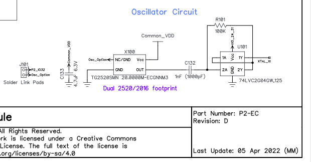
R35 and that open part you circled - these are for setting whether pin 4 of the 2016 footprint receives 3v3 for oscillator (as set up here), or GND for xtal. The original idea was a 0R or 1R resistor for measuring current draw
However, you're right in that we can and should put a cap there when configured like it is. It can only help.
@Tubular said:
R35 and that open part you circled - these are for setting whether pin 4 of the 2016 footprint receives 3v3 for oscillator (as set up here), or GND for xtal. The original idea was a 0R or 1R resistor for measuring current draw
However, you're right in that we can and should put a cap there when configured like it is. It can only help.
Yeah I think it would still work without it, just be less tolerant to noise on the supply. The solder joint seems okay too for XIN. When we probed it yesterday do you remember if we probed the 64MHz signal at R36 or on the P2 at the XOUT pin?
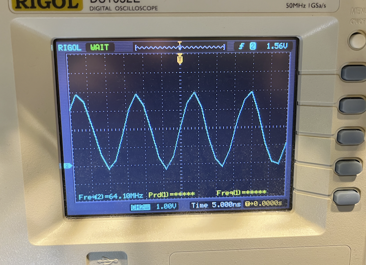
Just probed the XIN pin on the P2 and it does get the signal like we saw yesterday, nothing is coming out the XOUT pin. This was with the P2 idling after voltage initially applied - i.e. waiting on serial boot code so running in RCFAST mode. My crappy old bandwidth limited Rigol scope shows it around 64MHz. Overshoots up to 4V or so. Hopefully the P2 can handle that.
Just noticed on the P2 Edge RevD schematic that Parallax AC coupled the clock oscillator signal then fed through inverters. I wonder if this is because the P2 needed it for any reason or just to square up the edges a bit more?
UPDATE: can drive a LED from P30 so the VIO for that nibble seems okay.
PSRAM is functional at 24MHz (the only frequency I can test)
PSRAM memory read delay test over frequency, ESC exits
Enter the base pin number for your PSRAM (0,16,32,40) [40]: 32
Enter the chip enable pin number for your PSRAM [57]: 24
Enter the clock pin number for your PSRAM [56]: 57
Enter a starting frequency to test in MHz (24-350) : [24] 24
Enter the ending frequency to test in MHz (24-350) : [350] 24
Enter 1 to use the automatic delay value only, or 0 to test over the delay range : [0] 0
Enter 1 to display the first error encountered, or 0 to not display error details : [0] 0
Testing P2 from 24000000 - 24000000 Hz

            Successful data reads from 100 block transfers of 8192 random bytes
Frequency      Delay    3   4   5   6   7   8   9   10  11  12  13  14
24000000     (7)    0%  0%  100%    100%    100%    100%    0%  0%  0%  0%  0%  0%
Enter a starting frequency to test in MHz (24-350) : [24]
Exiting
I run some of my boards on a 50MHz clock from an ethernet MAC chip. So I don't see a reason why this shouldn't work with a 64MHz oscillator. I use theese settings
CON
  _xtlfreq = 50_000_000         ' master clock from Ethernet controller
  _clkfreq = 200_000_000
@Tubular said:
R35 and that open part you circled - these are for setting whether pin 4 of the 2016 footprint receives 3v3 for oscillator (as set up here), or GND for xtal. The original idea was a 0R or 1R resistor for measuring current draw
However, you're right in that we can and should put a cap there when configured like it is. It can only help.
Yeah I think it would still work without it, just be less tolerant to noise on the supply. The solder joint seems okay too for XIN. When we probed it yesterday do you remember if we probed the 64MHz signal at R36 or on the P2 at the XOUT pin?
We had the probe on the Xin pin of the P2. I didn't check Xout
@ManAtWork said:
I run some of my boards on a 50MHz clock from an ethernet MAC chip. So I don't see a reason why this shouldn't work with a 64MHz oscillator. I use theese settings
CON
  _xtlfreq = 50_000_000         ' master clock from Ethernet controller
  _clkfreq = 200_000_000
Ok, thats a super useful thing to know (and try), thanks ManAtWork.
@rogloh said:
So I think we left the XOUT pin still connected to the oscillator. If that 64MHz oscillator uses this pin for tri-state enable or something perhaps that would mess things up too. Would need it to be a NC internally.
Need to fix that, for sure. XO very much should be no-connect. Last CMOS oscillator I used had enable high on pin 1. It had internal pull-up so pin 1 could also be no-connect. Pin 2 GND, pin 3 CLK out, pin 4 Vcc. Looking at your photograph the numbering goes anticlockwise from top right.
Also, get rid of that resistor or capacitor from XI as well.
I think the reason the Edge Card uses the buffer circuit is because the oscillator is a "clipped sine" instead of CMOS. You might want to verify which type you have purchased too.
Yeah @ManAtWork I'd already tried that too. Although I am using flexspin not PNut in case that makes a difference. When that didn't work I started trying to control things manually and narrow down what frequency was actually operating by timing waitx loops and lighting LEDs.
E.g. for this code no serial output was seen and clock is slow to flash the LED - about 2.56MHz
CON
        _xtlfreq = 64_000_000
        _clkfreq = 256_000_000

OBJ
        uart:"SmartSerial"

PUB helloworld()
    pinl(54) ' light LED to say we are alive
    uart.start(115200)
    send:=@uart.tx

    ' send("hello",13,10) ' seemingly hangs if enabled

    org
        drvl #54
        rep #3, #0
        waitx ##1280000 ' flashes at ~1Hz?
        drvnot #54
        nop
    end
@evanh said:
I think the reason the Edge Card uses the buffer circuit is because the oscillator is a "clipped sine" instead of CMOS. You might want to verify which type you have purchased too.
It's a bit of mystery as to what device we actually have as far as pinouts...although it is generating a signal so it seems to be the fitted the right way around. I need to probe it now while running in PLL mode to see if it does something weird and shutoff temporarily or stretch every half clock cycle or something.
I just tried probing XI while operating on PLL, but of course it loads down the signal too much and the LED flashing pauses. However when I probe XO I do see a signal (which is buffered so it doesn't stop the flashing LED). Very weird looking signal.
I sort of wonder whether the XO is slowly charging the load cap until it hits a logic threshold voltage around 1.8V or so when it does something suddenly to enable the oscillator which soon afterwards is shutoff again (or vice versa). But this is on a scale far slower than the actual clocking of the oscillator. Weirdness.
Best guess is the flat top is how long it takes for the oscillator to transition from enabled to driving its output pin. The sharp falling edge is mirror of driven first leading edge on XI. Then the long low is probably the oscillator output tri-stated and falling slowly on XI until XO has again inverted back high.
@evanh said:
Best guess is the flat top is how long it takes for the oscillator to transition from enabled to driving its output pin. The sharp falling edge is mirror of driven first leading edge on XI. Then the long low is probably the oscillator output tri-stated and falling slowly on XI until XO has again inverted back high.
Yeah I reckon that's the likely cause of the issues. A tri-state or disabled oscillator condition, that weird rising edge points to something like that. I wonder if we can cut a trace on the board or if we need to wait for the real part (without tri-state)...? I could potentially lift the XO pin off the PCB too if I was careful.
LOL, it's very very small and a 6 layer board so risky. I'd be more likely to be able to lift the XO pin off the PCB with a sharp blade under it while heating with a fine iron tip. Don't really want to cut the XO pin off either in case we have to resort to a 20MHz xtal in the short term.
@rogloh said:
I just tried probing XI while operating on PLL, but of course it loads down the signal too much and the LED flashing pauses. However when I probe XO I do see a signal (which is buffered so it doesn't stop the flashing LED). Very weird looking signal.
I sort of wonder whether the XO is slowly charging the load cap until it hits a logic threshold voltage around 1.8V or so when it does something suddenly to enable the oscillator which soon afterwards is shutoff again (or vice versa). But this is on a scale far slower than the actual clocking of the oscillator. Weirdness.
This waveform defeats any logical explanation. The "shark fin" is in the wrong direction on the time scale! Any physical process like charging a capacitor starts with a steep slope and flattens out over time. Yours starts shallow and bends upward like a warped wall. Are you shure this isn't a sub-sampling effect of the scope?
@ManAtWork said:
I run some of my boards on a 50MHz clock from an ethernet MAC chip. So I don't see a reason why this shouldn't work with a 64MHz oscillator. I use theese settings
CON
  _xtlfreq = 50_000_000         ' master clock from Ethernet controller
  _clkfreq = 200_000_000
Ok, thats a super useful thing to know (and try), thanks ManAtWork.
Maybe we do need to cut XO track (which can be done). Looks like the osc has an 'output enable' function on pin 1 (=XO), with the output enabled when pin 1 is high or floating.
What we're seeing might be related to the startup time of the P2's OSC, when it gets going it outputs a low and this kills the external oscillator, whose output then falls to low over a relatively long time due to tristated output
The reason we might not have seen this is because we're too zoomed in on the cro, triggering off the burst, but if I'm right when we zoom out we should see the osc stopped most of the time, and 64 MHz for shortish bursts
@Tubular said:
Maybe we do need to cut XO track (which can be done). Looks like the osc has an 'output enable' function on pin 1 (=XO), with the output enabled when pin 1 is high or floating.
What we're seeing might be related to the startup time of the P2's OSC, when it gets going it outputs a low and this kills the external oscillator, whose output then falls to low over a relatively long time due to tristated output
The reason we might not have seen this is because we're too zoomed in on the cro, triggering off the burst, but if I'm right when we zoom out we should see the osc stopped most of the time, and 64 MHz for shortish bursts
When we scoped it initially we just let it run in RCFAST mode - this doesn't output anything on XO and the oscillator generates clocks nicely at 64MHz. But when I try to use XIN mode or the PLL mode there are problems because XO is an inverted/delayed copy of the input, buffered internally by the P2.
Yeah ok so that data sheet you found (thanks!) proves it now. Definitely XO has to be cut or lifted of the board. If there is nothing right under that track on the layers below I can potentially have a go at cutting it. Just didn't want to go too deep there and break something else below.
@ManAtWork said:
@rogloh said:
I just tried probing XI while operating on PLL, but of course it loads down the signal too much and the LED flashing pauses. However when I probe XO I do see a signal (which is buffered so it doesn't stop the flashing LED). Very weird looking signal.
I sort of wonder whether the XO is slowly charging the load cap until it hits a logic threshold voltage around 1.8V or so when it does something suddenly to enable the oscillator which soon afterwards is shutoff again (or vice versa). But this is on a scale far slower than the actual clocking of the oscillator. Weirdness.
This waveform defeats any logical explanation. The "shark fin" is in the wrong direction on the time scale! Any physical process like charging a capacitor starts with a steep slope and flattens out over time. Yours starts shallow and bends upward like a warped wall. Are you shure this isn't a sub-sampling effect of the scope?
I agree and also noticed that too myself - it's a very strange accelerating non-linear shape vs a normal RC charging curve. As to sub-sampling at 33kHz can't be sure there but I know the capacitive effect of the scope probe itself will certainly affect things as well. Plus I noticed when I changed the cc bits affecting capacitance loads it also affected the frequency in the results yesterday. Got slower when more capacitance was added, as the charge is retained for longer when it tri-states the output.
Some success I think. I was able to lightly cut through the XO track to the oscillator according to this zoomed in and now blurry image. Now it takes 32 million waitx cycles to flash at 1Hz (which is half a second between toggles). I also noticed the current draw increased significantly when I enabled the 64MHz clock source using XIN up to 40mA from 6mA or so before. Now I can mess with PLL settings to see what I can achieve.
@evanh said:
SOME??! That's complete success! :P And well done on the handy work. That's a mighty small nick. Those pins are only 0.25 mm think.
Thanks - I hope it's good. There is a ground plane directly under so if that shorted to the exposed trace it could disable the oscillator. So far it seems okay.
I'm running it at 256MHz now with the PLL. Current is 117mA with a single COG flat out doing waitx LED flashing with 2x128M cycle waitx intervals for 1Hz. So I should be able to test PSRAM at speed now.
Tested PSRAM at >300MHz and see it doing something weird and hanging the test program once it reaches around 328MHz. I've never seen that before, normally if PSRAM read/write test fails the test continues on and just reports 0%. The current draw was around 191mA from a 5V supply during the test and just before/as it hangs I noticed it jumps to 207mA before locking up and then remaining at that load. Current limit is set to 500mA on my supply so it's not doing current limiting. Not sure if it is a regulator issue. I should probe the 1.8 and 3.3V output voltages if I can get to them. EDIT: 3.46V and 1.73V so they appear reasonable, unless 1.73V is not sufficient for 328MHz operation.
PSRAM memory read delay test over frequency, ESC exits
Enter the base pin number for your PSRAM (0,16,32,40) [40]: 32
Enter the chip enable pin number for your PSRAM [57]: 24
Enter the clock pin number for your PSRAM [56]: 57
Enter a starting frequency to test in MHz (24-350) : [24] 320
Enter the ending frequency to test in MHz (320-350) : [350] 350
Enter 1 to use the automatic delay value only, or 0 to test over the delay range : [0] 0
Enter 1 to display the first error encountered, or 0 to not display error details : [0] 0
Testing P2 from 320000000 - 350000000 Hz

                        Successful data reads from 100 block transfers of 8192 random bytes
Frequency      Delay    3       4       5       6       7       8       9       10      11      12      13      14
320000000        (12)   0%      0%      0%      0%      0%      0%      0%      35%     100%    100%    100%    0%
321000000        (12)   0%      0%      0%      0%      0%      0%      0%      3%      100%    100%    100%    0%
322000000        (12)   0%      0%      0%      0%      0%      0%      0%      0%      100%    100%    100%    0%
323000000        (12)   0%      0%      0%      0%      0%      0%      0%      0%      100%    100%    100%    0%
324000000        (12)   0%      0%      0%      0%      0%      0%      0%      0%      100%    100%    100%    0%
325000000        (12)   0%      0%      0%      0%      0%      0%      0%      0%      100%    100%    100%    0%
326000000        (12)   0%      0%      0%      0%      0%      0%      0%      0%      100%    100%    100%    0%
327000000        (12)   0%      0%      0%      0%      0%      0%      0%      0%      100%    100%    100%    0%
328000000        (12)   0%      0%      0%      0%      0%      0%      0%      0%      93%     91%     94%     0%
329000000        (12)   %

Testing P2 from 320000000 - 350000000 Hz

                        Successful data reads from 100 block transfers of 8192 random bytes
Frequency      Delay    3       4       5       6       7       8       9       10      11      12      13      14
320000000        (12)   0%      0%      0%      0%      0%      0%      0%      5%      100%    100%    100%    0%
321000000        (12)   0%      0%      0%      0%      0%      0%      0%      0%      100%    100%    100%    0%
322000000        (12)   0%      0%      0%      0%      0%      0%      0%      0%      100%    100%    100%    0%
323000000        (12)   0%      0%      0%      0%      0%      0%      0%      0%      100%    100%    100%    0%
324000000        (12)   0%      0%      0%      0%      0%      0%      0%      0%      100%    100%    100%    0%
325000000        (12)   0%      0%      0%      0%      0%      0%      0%      0%      100%    100%    100%    0%
326000000        (12)   0%      0%      0%      0%      0%      0%      0%      0%      99%     100%    100%    0%
327000000        (12)   0%      0%      0%      0%      0%      0%      0%      0%      43%     43%     36%     0%
328000000        (12)   %

Testing P2 from 320000000 - 350000000 Hz

                        Successful data reads from 100 block transfers of 8192 random bytes
Frequency      Delay    3       4       5       6       7       8       9       10      11      12      13      14
320000000        (12)   0%      0%      0%      0%      0%      0%      0%      5%      100%    100%    100%    0%
321000000        (12)   0%      0%      0%      0%      0%      0%      0%      0%      100%    100%    100%    0%
322000000        (12)   0%      0%      0%      0%      0%      0%      0%      0%      100%    100%    100%    0%
323000000        (12)   0%      0%      0%      0%      0%      0%      0%      0%      100%    100%    100%    0%
324000000        (12)   0%      0%      0%      0%      0%      0%      0%      0%      100%    100%    100%    0%
325000000        (12)   0%      0%      0%      0%      0%      0%      0%      0%      100%    100%    100%    0%
326000000        (12)   0%      0%      0%      0%      0%      0%      0%      0%      97%     98%     95%     0%
327000000        (12)   0%      %
@rogloh said:
... 3.46V and 1.73V so they appear reasonable, unless 1.73V is not sufficient for 328MHz operation.
That'll be it. Rayman did a lot of good testing of this very thing and found that a raised voltage of the 1.8V rail is very important for reliable overclocking. He now targets 1.9 Volts I believe. I remember thinking it made a lot of sense in hindsight, even though I'd never tried testing it myself.
The threshold for reliable hubRAM read/write will lower as the voltage is decreased. Just as it also does the same as temperature is increased.
Yeah I went over to Tubular's again today and we tweaked a regulator feedback resistor and now get over 1.8V on the P2 VDD rail (EDIT: 1.86V) and the memory is working up to 350MHz! This is with 32MB fitted. Adding the other 32MB will drop this down of course so I may not do that for a while yet.
Here are the results - the window tightens up towards 350MHz. But I'm hoping it'll still be okay for Wuerfel_21's emulators.
Just ran @evanh SD card test with 100 files on my FireAnt board with the basepin set to 48. From this it seems to be working I think. No errors reported. Now I just need to plug it into the GPi 2W and modify the pin (and clock) settings from the first proof of concept variant of this and it should let me run Ada's emulators with any luck.
❯ loadp2 -t -b 230400 sdfat-accesstest.binary
( Entering terminal mode. Press Ctrl-] or Ctrl-Z to exit. )


Comments
@Tubular I do see what looks to be a missing cap in the close up microscope image below. This cap is in parallel with the bypass cap for VIO28_31 on P2 pin number 47. Maybe the oscillator would work better with the extra one fitted? Perhaps with the oscillator's current draw and HF bouncing signals the existing 2.2uF bypass cap is insufficient? I buzzed out the wiring on a spare board and follow the paths, then buzzed out the real board and it all appears to connect ok through those zero ohm resistors. Hopefully the footprint for this particular type of oscillator we got is correct and we don't feed the signal into XOUT instead of XIN or something. I'll also try to probe which P2 pin(s) see the 64MHz soon. The XOUT probably has a replica of the signal though if the P2's PLL clock mode is enabled - will need to keep that off too when probing.
Also the P2 doc mentions this...
So I think we left the XOUT pin still connected to the oscillator. If that 64MHz oscillator uses this pin for tri-state enable or something perhaps that would mess things up too. Would need it to be a NC internally.
R35 and that open part you circled - these are for setting whether pin 4 of the 2016 footprint receives 3v3 for oscillator (as set up here), or GND for xtal. The original idea was a 0R or 1R resistor for measuring current draw
However, you're right in that we can and should put a cap there when configured like it is. It can only help.
Yeah I think it would still work without it, just be less tolerant to noise on the supply. The solder joint seems okay too for XIN. When we probed it yesterday do you remember if we probed the 64MHz signal at R36 or on the P2 at the XOUT pin?
Just probed the XIN pin on the P2 and it does get the signal like we saw yesterday, nothing is coming out the XOUT pin. This was with the P2 idling after voltage initially applied - i.e. waiting on serial boot code so running in RCFAST mode. My crappy old bandwidth limited Rigol scope shows it around 64MHz. Overshoots up to 4V or so. Hopefully the P2 can handle that.
Just noticed on the P2 Edge RevD schematic that Parallax AC coupled the clock oscillator signal then fed through inverters. I wonder if this is because the P2 needed it for any reason or just to square up the edges a bit more?
UPDATE: can drive a LED from P30 so the VIO for that nibble seems okay.
PSRAM is functional at 24MHz (the only frequency I can test)
PSRAM memory read delay test over frequency, ESC exits Enter the base pin number for your PSRAM (0,16,32,40) [40]: 32 Enter the chip enable pin number for your PSRAM [57]: 24 Enter the clock pin number for your PSRAM [56]: 57 Enter a starting frequency to test in MHz (24-350) : [24] 24 Enter the ending frequency to test in MHz (24-350) : [350] 24 Enter 1 to use the automatic delay value only, or 0 to test over the delay range : [0] 0 Enter 1 to display the first error encountered, or 0 to not display error details : [0] 0 Testing P2 from 24000000 - 24000000 Hz Successful data reads from 100 block transfers of 8192 random bytes Frequency Delay 3 4 5 6 7 8 9 10 11 12 13 14 24000000 (7) 0% 0% 100% 100% 100% 100% 0% 0% 0% 0% 0% 0% Enter a starting frequency to test in MHz (24-350) : [24] ExitingI run some of my boards on a 50MHz clock from an ethernet MAC chip. So I don't see a reason why this shouldn't work with a 64MHz oscillator. I use theese settings
We had the probe on the Xin pin of the P2. I didn't check Xout
Ok, thats a super useful thing to know (and try), thanks ManAtWork.
Need to fix that, for sure. XO very much should be no-connect. Last CMOS oscillator I used had enable high on pin 1. It had internal pull-up so pin 1 could also be no-connect. Pin 2 GND, pin 3 CLK out, pin 4 Vcc. Looking at your photograph the numbering goes anticlockwise from top right.
Also, get rid of that resistor or capacitor from XI as well.
I think the reason the Edge Card uses the buffer circuit is because the oscillator is a "clipped sine" instead of CMOS. You might want to verify which type you have purchased too.
Yeah @ManAtWork I'd already tried that too. Although I am using flexspin not PNut in case that makes a difference. When that didn't work I started trying to control things manually and narrow down what frequency was actually operating by timing waitx loops and lighting LEDs.
E.g. for this code no serial output was seen and clock is slow to flash the LED - about 2.56MHz
CON _xtlfreq = 64_000_000 _clkfreq = 256_000_000 OBJ uart:"SmartSerial" PUB helloworld() pinl(54) ' light LED to say we are alive uart.start(115200) send:=@uart.tx ' send("hello",13,10) ' seemingly hangs if enabled org drvl #54 rep #3, #0 waitx ##1280000 ' flashes at ~1Hz? drvnot #54 nop endIt's a bit of mystery as to what device we actually have as far as pinouts...although it is generating a signal so it seems to be the fitted the right way around. I need to probe it now while running in PLL mode to see if it does something weird and shutoff temporarily or stretch every half clock cycle or something.
I just tried probing XI while operating on PLL, but of course it loads down the signal too much and the LED flashing pauses. However when I probe XO I do see a signal (which is buffered so it doesn't stop the flashing LED). Very weird looking signal.
I sort of wonder whether the XO is slowly charging the load cap until it hits a logic threshold voltage around 1.8V or so when it does something suddenly to enable the oscillator which soon afterwards is shutoff again (or vice versa). But this is on a scale far slower than the actual clocking of the oscillator. Weirdness.
Best guess is the flat top is how long it takes for the oscillator to transition from enabled to driving its output pin. The sharp falling edge is mirror of driven first leading edge on XI. Then the long low is probably the oscillator output tri-stated and falling slowly on XI until XO has again inverted back high.
Yeah I reckon that's the likely cause of the issues. A tri-state or disabled oscillator condition, that weird rising edge points to something like that. I wonder if we can cut a trace on the board or if we need to wait for the real part (without tri-state)...? I could potentially lift the XO pin off the PCB too if I was careful.
Looks easy to cut the track at XO pin with it magnified like that.
LOL, it's very very small and a 6 layer board so risky. I'd be more likely to be able to lift the XO pin off the PCB with a sharp blade under it while heating with a fine iron tip. Don't really want to cut the XO pin off either in case we have to resort to a 20MHz xtal in the short term.
This waveform defeats any logical explanation. The "shark fin" is in the wrong direction on the time scale! Any physical process like charging a capacitor starts with a steep slope and flattens out over time. Yours starts shallow and bends upward like a warped wall. Are you shure this isn't a sub-sampling effect of the scope?
Ok, thats a super useful thing to know (and try), thanks ManAtWork.
Maybe we do need to cut XO track (which can be done). Looks like the osc has an 'output enable' function on pin 1 (=XO), with the output enabled when pin 1 is high or floating.
What we're seeing might be related to the startup time of the P2's OSC, when it gets going it outputs a low and this kills the external oscillator, whose output then falls to low over a relatively long time due to tristated output
The reason we might not have seen this is because we're too zoomed in on the cro, triggering off the burst, but if I'm right when we zoom out we should see the osc stopped most of the time, and 64 MHz for shortish bursts
Here's the datasheet https://www.lcsc.com/datasheet/C3034268.pdf
When we scoped it initially we just let it run in RCFAST mode - this doesn't output anything on XO and the oscillator generates clocks nicely at 64MHz. But when I try to use XIN mode or the PLL mode there are problems because XO is an inverted/delayed copy of the input, buffered internally by the P2.
Yeah ok so that data sheet you found (thanks!) proves it now. Definitely XO has to be cut or lifted of the board. If there is nothing right under that track on the layers below I can potentially have a go at cutting it. Just didn't want to go too deep there and break something else below.
I agree and also noticed that too myself - it's a very strange accelerating non-linear shape vs a normal RC charging curve. As to sub-sampling at 33kHz can't be sure there but I know the capacitive effect of the scope probe itself will certainly affect things as well. Plus I noticed when I changed the cc bits affecting capacitance loads it also affected the frequency in the results yesterday. Got slower when more capacitance was added, as the charge is retained for longer when it tri-states the output.
Some success I think. I was able to lightly cut through the XO track to the oscillator according to this zoomed in and now blurry image. Now it takes 32 million waitx cycles to flash at 1Hz (which is half a second between toggles). I also noticed the current draw increased significantly when I enabled the 64MHz clock source using XIN up to 40mA from 6mA or so before. Now I can mess with PLL settings to see what I can achieve.
SOME??! That's complete success! :P And well done on the handy work. That's a mighty small nick. Those pins are only 0.25 mm wide.
Thanks - I hope it's good. There is a ground plane directly under so if that shorted to the exposed trace it could disable the oscillator. So far it seems okay.
I'm running it at 256MHz now with the PLL. Current is 117mA with a single COG flat out doing waitx LED flashing with 2x128M cycle waitx intervals for 1Hz. So I should be able to test PSRAM at speed now.
Great news, may you enjoy continued success...
👍
Tested PSRAM at >300MHz and see it doing something weird and hanging the test program once it reaches around 328MHz. I've never seen that before, normally if PSRAM read/write test fails the test continues on and just reports 0%. The current draw was around 191mA from a 5V supply during the test and just before/as it hangs I noticed it jumps to 207mA before locking up and then remaining at that load. Current limit is set to 500mA on my supply so it's not doing current limiting. Not sure if it is a regulator issue. I should probe the 1.8 and 3.3V output voltages if I can get to them. EDIT: 3.46V and 1.73V so they appear reasonable, unless 1.73V is not sufficient for 328MHz operation.
PSRAM memory read delay test over frequency, ESC exits Enter the base pin number for your PSRAM (0,16,32,40) [40]: 32 Enter the chip enable pin number for your PSRAM [57]: 24 Enter the clock pin number for your PSRAM [56]: 57 Enter a starting frequency to test in MHz (24-350) : [24] 320 Enter the ending frequency to test in MHz (320-350) : [350] 350 Enter 1 to use the automatic delay value only, or 0 to test over the delay range : [0] 0 Enter 1 to display the first error encountered, or 0 to not display error details : [0] 0 Testing P2 from 320000000 - 350000000 Hz Successful data reads from 100 block transfers of 8192 random bytes Frequency Delay 3 4 5 6 7 8 9 10 11 12 13 14 320000000 (12) 0% 0% 0% 0% 0% 0% 0% 35% 100% 100% 100% 0% 321000000 (12) 0% 0% 0% 0% 0% 0% 0% 3% 100% 100% 100% 0% 322000000 (12) 0% 0% 0% 0% 0% 0% 0% 0% 100% 100% 100% 0% 323000000 (12) 0% 0% 0% 0% 0% 0% 0% 0% 100% 100% 100% 0% 324000000 (12) 0% 0% 0% 0% 0% 0% 0% 0% 100% 100% 100% 0% 325000000 (12) 0% 0% 0% 0% 0% 0% 0% 0% 100% 100% 100% 0% 326000000 (12) 0% 0% 0% 0% 0% 0% 0% 0% 100% 100% 100% 0% 327000000 (12) 0% 0% 0% 0% 0% 0% 0% 0% 100% 100% 100% 0% 328000000 (12) 0% 0% 0% 0% 0% 0% 0% 0% 93% 91% 94% 0% 329000000 (12) % Testing P2 from 320000000 - 350000000 Hz Successful data reads from 100 block transfers of 8192 random bytes Frequency Delay 3 4 5 6 7 8 9 10 11 12 13 14 320000000 (12) 0% 0% 0% 0% 0% 0% 0% 5% 100% 100% 100% 0% 321000000 (12) 0% 0% 0% 0% 0% 0% 0% 0% 100% 100% 100% 0% 322000000 (12) 0% 0% 0% 0% 0% 0% 0% 0% 100% 100% 100% 0% 323000000 (12) 0% 0% 0% 0% 0% 0% 0% 0% 100% 100% 100% 0% 324000000 (12) 0% 0% 0% 0% 0% 0% 0% 0% 100% 100% 100% 0% 325000000 (12) 0% 0% 0% 0% 0% 0% 0% 0% 100% 100% 100% 0% 326000000 (12) 0% 0% 0% 0% 0% 0% 0% 0% 99% 100% 100% 0% 327000000 (12) 0% 0% 0% 0% 0% 0% 0% 0% 43% 43% 36% 0% 328000000 (12) % Testing P2 from 320000000 - 350000000 Hz Successful data reads from 100 block transfers of 8192 random bytes Frequency Delay 3 4 5 6 7 8 9 10 11 12 13 14 320000000 (12) 0% 0% 0% 0% 0% 0% 0% 5% 100% 100% 100% 0% 321000000 (12) 0% 0% 0% 0% 0% 0% 0% 0% 100% 100% 100% 0% 322000000 (12) 0% 0% 0% 0% 0% 0% 0% 0% 100% 100% 100% 0% 323000000 (12) 0% 0% 0% 0% 0% 0% 0% 0% 100% 100% 100% 0% 324000000 (12) 0% 0% 0% 0% 0% 0% 0% 0% 100% 100% 100% 0% 325000000 (12) 0% 0% 0% 0% 0% 0% 0% 0% 100% 100% 100% 0% 326000000 (12) 0% 0% 0% 0% 0% 0% 0% 0% 97% 98% 95% 0% 327000000 (12) 0% %That'll be it. Rayman did a lot of good testing of this very thing and found that a raised voltage of the 1.8V rail is very important for reliable overclocking. He now targets 1.9 Volts I believe. I remember thinking it made a lot of sense in hindsight, even though I'd never tried testing it myself.
The threshold for reliable hubRAM read/write will lower as the voltage is decreased. Just as it also does the same as temperature is increased.
Yeah I went over to Tubular's again today and we tweaked a regulator feedback resistor and now get over 1.8V on the P2 VDD rail (EDIT: 1.86V) and the memory is working up to 350MHz! This is with 32MB fitted. Adding the other 32MB will drop this down of course so I may not do that for a while yet.
Here are the results - the window tightens up towards 350MHz. But I'm hoping it'll still be okay for Wuerfel_21's emulators.
Testing P2 from 320000000 - 350000000 Hz Successful data reads from 100 block transfers of 8192 random bytes Frequency Delay 3 4 5 6 7 8 9 10 11 12 13 14 320000000 (12) 0% 0% 0% 0% 0% 0% 0% 94% 100% 100% 100% 0% 321000000 (12) 0% 0% 0% 0% 0% 0% 0% 88% 100% 100% 100% 0% 322000000 (12) 0% 0% 0% 0% 0% 0% 0% 70% 100% 100% 100% 0% 323000000 (12) 0% 0% 0% 0% 0% 0% 0% 29% 100% 100% 100% 0% 324000000 (12) 0% 0% 0% 0% 0% 0% 0% 1% 100% 100% 100% 0% 325000000 (12) 0% 0% 0% 0% 0% 0% 0% 0% 100% 100% 100% 0% 326000000 (12) 0% 0% 0% 0% 0% 0% 0% 0% 100% 100% 100% 0% 327000000 (12) 0% 0% 0% 0% 0% 0% 0% 0% 100% 100% 100% 0% 328000000 (12) 0% 0% 0% 0% 0% 0% 0% 0% 100% 100% 100% 0% 329000000 (12) 0% 0% 0% 0% 0% 0% 0% 0% 100% 100% 100% 0% 330000000 (12) 0% 0% 0% 0% 0% 0% 0% 0% 100% 100% 100% 0% 331000000 (12) 0% 0% 0% 0% 0% 0% 0% 0% 100% 100% 100% 0% 332000000 (12) 0% 0% 0% 0% 0% 0% 0% 0% 100% 100% 100% 0% 333000000 (13) 0% 0% 0% 0% 0% 0% 0% 0% 100% 100% 100% 0% 334000000 (13) 0% 0% 0% 0% 0% 0% 0% 0% 99% 100% 100% 0% 335000000 (13) 0% 0% 0% 0% 0% 0% 0% 0% 96% 100% 100% 0% 336000000 (13) 0% 0% 0% 0% 0% 0% 0% 0% 90% 100% 100% 0% 337000000 (13) 0% 0% 0% 0% 0% 0% 0% 0% 94% 100% 100% 0% 338000000 (13) 0% 0% 0% 0% 0% 0% 0% 0% 94% 99% 100% 0% 339000000 (13) 0% 0% 0% 0% 0% 0% 0% 0% 63% 86% 100% 0% 340000000 (13) 0% 0% 0% 0% 0% 0% 0% 0% 27% 24% 100% 0% 341000000 (13) 0% 0% 0% 0% 0% 0% 0% 0% 2% 0% 100% 0% 342000000 (13) 0% 0% 0% 0% 0% 0% 0% 0% 0% 0% 100% 0% 343000000 (13) 0% 0% 0% 0% 0% 0% 0% 0% 0% 0% 100% 0% 344000000 (13) 0% 0% 0% 0% 0% 0% 0% 0% 0% 0% 100% 0% 345000000 (13) 0% 0% 0% 0% 0% 0% 0% 0% 0% 0% 100% 0% 346000000 (13) 0% 0% 0% 0% 0% 0% 0% 0% 0% 0% 100% 0% 347000000 (13) 0% 0% 0% 0% 0% 0% 0% 0% 0% 0% 100% 0% 348000000 (13) 0% 0% 0% 0% 0% 0% 0% 0% 0% 0% 100% 0% 349000000 (13) 0% 0% 0% 0% 0% 0% 0% 0% 0% 0% 100% 0% 350000000 (13) 0% 0% 0% 0% 0% 0% 0% 0% 0% 0% 100% 0%Just ran @evanh SD card test with 100 files on my FireAnt board with the basepin set to 48. From this it seems to be working I think. No errors reported. Now I just need to plug it into the GPi 2W and modify the pin (and clock) settings from the first proof of concept variant of this and it should let me run Ada's emulators with any luck.
❯ loadp2 -t -b 230400 sdfat-accesstest.binary
( Entering terminal mode. Press Ctrl-] or Ctrl-Z to exit. )
clkfreq = 128000000 clkmode = 0x10001fb
/sd1 handle = ce4c ... mounted
Delete 100 files ... Duration 253 ms, 395.2 files/s
File size = 512 bytes
Create 100 files ... Duration 3912 ms, 25.5 files/s
Verify 100 files ... Duration 355 ms, 281.6 files/s
Clean-up ... errno = 0: OK