

Sunnyside the FLiP compatible P2 module
 SaucySoliton
Posts: 568
SaucySoliton
Posts: 568
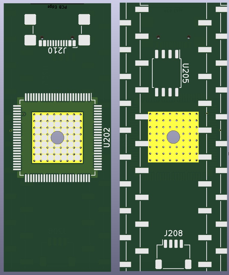
Great for breadboard use or as an upgrade for designs using FLiP or a DIP 40 P1. Will be slightly wider than a FLiP or DIP 40.
USB-C connector with data pins P62, P63. Reset signal on USB SBU pins. For now it would work with special prop plug with type C output. In the future we could have a native USB bootloader. I think an FTDI chip would fit on there if desired.
At the other end maybe a 4 pin JST for I2C. (QWIIC) If the PCB is 0.8 to 1mm thick then an edge connector for an HDMI cable is possible. Or another USB-C connector so the Sunnyside and Prop-Plug-C are the same board.
Power supply would generate the 1.8v from the 3.3v since the P1 only receives 3.3v. If used in place of a FLiP it would accept 5-9v from the appropriate pin.
Not routed yet, but I think it's possible with 4 layers.
Comments
Interesting idea. Wonder if all the Parallax style 0402 caps could fit on there. Maybe...
Nice!
A usb-serial chip will make it complete and a SD card slot will enhance it greatly.
Neat idea. If you have room somewhere eg. down near your potential HDMI connector (full size or micro?), a spare SOP8 footprint for devices with 6 free IO available could be useful for anyone interested in soldering in some optional additional flash or PSRAM device etc, as such spare memory is always useful for video, or for emulation applications. Certainly PCB real estate will start to get tight once you start routing and adding such features however.
Maybe the KISS board gives some inspiration
3 pins longer than a Pi Pico
16 MB PSRAM optional
2 EVAL connectors
USB-C upstream and downstream allows the same product to be used as a prog plug (with type C) or target board.
Interesting sacrifice of some through hole pins at the closest side to the P2 to keep the width in check.
How much total IO do you intend to bring out? Looks like it could do something similar to P2-EC32MB ~40 GPIO pins or so, maybe a few more.
This is my take at a low cost P2 board.
Mostly Pi Pico compatible pinout. It's a bit longer.
Single sided pick and place (except PSRAM. Although overclocking might not be great with capacitors on 2 edges only.)
Breadboard compatible .1" through hole headers. I think it would be possible to bend some of the top pins to connect to the castellated edge and get all of the pins.
Uses the P2 internal crystal oscillator to save a few cents and lower standby power.
USB-C connector for programming. I think a native USB bootloader is possible. Until that happens, those pins can be used for the usual serial programming.
A second USB-C connector to program another board or connect to USB devices.
4 layer board without via-in-pad.
7 pins lost due to lack of space to route them. (Pins 0-3, 38-39, 47)
10 pins PSRAM (48-57)
4 pins flash (58-61)
41 total GPIO, including P62-63. 29 on a breadboard, 33 castellated. (Pico has 26)
2 pins dedicated to QWIIC connector. (32-33)
2 EVAL connectors, 1 with 5v power
Pins starting with B are the inside columns.
I pivoted towards Pico compatible instead of FLiP compatible. But I still really like the Sunnyside name.
Hi
That looks good!
For my projects an SD card holder is much more useful than a second USB though....
Christof
Looks useful, nice that it's breadboard-able. Given the proximity you might be able to add extra PropPlug holes with tweaks along top edge in case you need some initial programming without custom USB-C cable availability and before USB capable bootloader is installed into the flash.
Still keep it simple, not every feature and /or pin out is needed on the P2 FLIP module. My concern / problem has been the fan out /_PCB real estate used for all the P2 i/o pins for my PCB layout application. In other words, use header connections on the "top side" of the P2 FLIP module for things like a Key pad, LCD display module, VGA or HDMI video, fitted with a ribbon cable arrangement. Consider 8 or 16 pin groupings for this.
Nice to have, but not necessary: uSD card socket, 16 MB SPI Flash, only one USB-C connection, no JST connectors, Internal VDD Power Supply(s)
Remember, it is up to the PCB layout and engineer /programmer, to make the best use of any uP and features, and adapt as necessary
Gave up one EVAL header to fit the micro SD card. 4 bit interface.
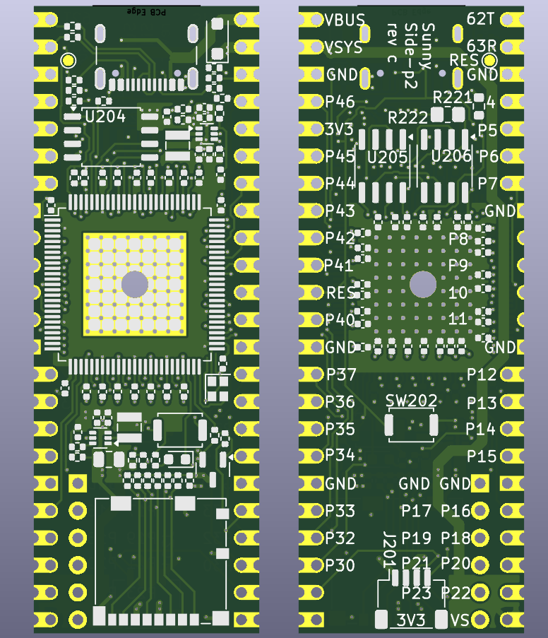
Prop plug header could be attached to the board with some creative soldering.