@Rayman said:
@rogloh Your 64 MB layout had two CS and two clocks, right? One CS for each 16-bit bank. Clocks for each 8-bit half bus. Guess that lets you address as four independent 8-bit banks.
Yeah definitely two of each but I'd need to go back and verify my layout. With what I mentioned I believe you could theoretically run independent 8 bit buses but with only half the total memory accessible (so 32MB of the 64MB), although I've not done this so far. Or when you setup the pingroup count as 1 for the clock pin, it will drive two clock signals (one for each 8 bits) and allow 16 bit transfers. That's how you could access the full bandwidth from a single driver COG. The second CS could be used to access the upper 32MB in this case. I think this is correct but I'm a little rusty nowadays because I've not be messing with PSRAM a lot recently.
@Rayman said:
@evanh Honestly, I've just been using same parts as Parallax (at least I think). APS6404L-3SQR-SN
What part# does DDR?
Well, one of the difficulties is they're the same BGA footprint as the HyperBus parts. See my previous mock-up. The pad spacings are very tight. I had to adjust minimum layout clearances and reduce via size just to place single vias in the diagonals.
EDIT: And are same pinout too. They are electrically drop-in compatible with HyperRAMs but use an OctoSPI protocol whereas HyperRAMs use more of a multiplexed Address/Data setup more like SDRAMs.
@Rayman said:
Ok, got the 64 MB of PSRAM wired up. Not sure could have done it without the extra two layers...
That looks to have caps on top and bottom ?
It may be better to remove most of the top side ones, to allow shorter traces, and you could add solder bridge jumpers to the RAM leads to connectors to reduce the C+Stub Load for RAM only board
I see there are Cap arrays available, in 0805 and 1206 packages - the 2 caps in 0805 look to fit well, and are more manageable than 4-caps, as they have 1mm lead pitch and the pair-repeat pitch is 3.0mm from P2 so the 2mm package has 1mm clearance.
A custom footprint could allow via-in-pad for even shorter decoupling lead lengths. The P2 exit pitch is 1.5mm, CAP pad pitch is 1.0mm, but the package is long enough to allow 1.5mm cap pad entry.
@Rayman , I just buzzed out my old 64MB PSRAM board and found I was incorrect about having 4 control pins. Turns out I actually wired up 8 control pins plus 16 data pins on this PCB. There were 4 chip selects and 4 clocks.
If PSRAMs are attached to P2 data pins and labeled this way for example:
D0..D3 : IC1 & IC5
D4..D7 : IC2 & IC6
D8..D11 : IC3 & IC7
D12..D15 : IC4 & IC8
Then the control pins were done like this (in this order)
CS1 - wired to IC1 & IC2
CS2 - wired to IC3 & IC4
CLK1 - wired to IC1 & IC2
CLK2 - wired to IC3 & IC4
CS3 - wired to IC5 & IC6
CS4 - wired to IC7 & IC8
CLK3 - wired to IC5 & IC6
CLK4 - wired to IC7 & IC8
But I think you can do it with 4 signals, they'll just increase the fanout for each signal by 2x. For CS it's fine but the clock signal could be more of an issue and would be loaded up more. It may required different tuning. So long as it remains valid as a clock the delay can be tuned accordingly. The P2 Edge gets away with a fanout of 4 devices for it's 32MB implementation so you should be fine.
Update: One more thing to consider. You don't want to end up in a situation where some clock signals are delayed far more than others to the point where you can't find a sweet spot timing delay value that works for both PSRAM byte lanes. So trying to match impedance and lengths to some degree is wise for the clocks (as well as data bits of course).
@Rayman said:
@SaucySoliton See post #20, there are now very short run caps on bottom of board, if needed.
Sorry, I didn't see that. That is much better. I remember a discussion here that physically smaller bypass capacitors have lower impedance. That's why the Parallax boards have 4.7uF 0402 caps. If you can comfortably solder smaller capacitors that should help a bit.
Hopefully the choice to use P28-P31 for the control lines and high speed clock won't come back to bite you later. If it were me I'd have used P48-P51 for those signals to not mess with the PLL IO supply on that nibble.
The high frequency decoupling caps look a tad spread out. If you're placing any components on the underside of the board then they should definitely be there too. The existing VDD/VIO vias can pop straight through to said caps.
@SaucySoliton said:
Sorry, I didn't see that. That is much better. I remember a discussion here that physically smaller bypass capacitors have lower impedance. That's why the Parallax boards have 4.7uF 0402 caps. If you can comfortably solder smaller capacitors that should help a bit.
@Rayman said:
The MLCC all have about the same ESR. But, it's actually the RC time that matters and I think that manifests as the resonant frequency.
I don't think 4.7 uF caps can help with high frequency noise...
Above the resonant notch, the impedance is inductance determined, and the cap vendor plots exclude pcb traces, that's why very short leads to the C is important, and some designs use via-in-pad.
The ideal placement for decoupling is 'under the package' so the VCC-CAP-GND loop is smallest area.
On your PSRAMs it looks like you can improve that, as you already have the caps on the other side
@Rayman said:
Got MegaYume beta 05 running with onboard PSRAM.
beta 05, that's ancient. Better upgrade that. Also, give the usbnew branch on either emulator a try for USB Hub support. (Also MegaYume has a bug fix that I did on that branch because I'm lazy)
That's kind of nice because thing only need 1 chip for that to work...
If you're using 16 or 8 bit mode it does use all the chips in the bank.


Comments
Yeah definitely two of each but I'd need to go back and verify my layout. With what I mentioned I believe you could theoretically run independent 8 bit buses but with only half the total memory accessible (so 32MB of the 64MB), although I've not done this so far. Or when you setup the pingroup count as 1 for the clock pin, it will drive two clock signals (one for each 8 bits) and allow 16 bit transfers. That's how you could access the full bandwidth from a single driver COG. The second CS could be used to access the upper 32MB in this case. I think this is correct but I'm a little rusty nowadays because I've not be messing with PSRAM a lot recently.
@evanh Honestly, I've just been using same parts as Parallax (at least I think). APS6404L-3SQR-SN
What part# does DDR?
Ok, got the 64 MB of PSRAM wired up. Not sure could have done it without the extra two layers...
Now that I think about it though, seems I have lower clock on Port A and upper clock on Port B.
That's a problem, right?
Yes, I think so. The clock and select pins each need to be in a contiguous addpins range (and therefore can't cross the port boundary)
Ok, redid the clock/select wiring like this
Well, one of the difficulties is they're the same BGA footprint as the HyperBus parts. See my previous mock-up. The pad spacings are very tight. I had to adjust minimum layout clearances and reduce via size just to place single vias in the diagonals.
EDIT: And are same pinout too. They are electrically drop-in compatible with HyperRAMs but use an OctoSPI protocol whereas HyperRAMs use more of a multiplexed Address/Data setup more like SDRAMs.
That looks to have caps on top and bottom ?
It may be better to remove most of the top side ones, to allow shorter traces, and you could add solder bridge jumpers to the RAM leads to connectors to reduce the C+Stub Load for RAM only board
I see there are Cap arrays available, in 0805 and 1206 packages - the 2 caps in 0805 look to fit well, and are more manageable than 4-caps, as they have 1mm lead pitch and the pair-repeat pitch is 3.0mm from P2 so the 2mm package has 1mm clearance.
A custom footprint could allow via-in-pad for even shorter decoupling lead lengths. The P2 exit pitch is 1.5mm, CAP pad pitch is 1.0mm, but the package is long enough to allow 1.5mm cap pad entry.
Ok, I forgot about caps..
I’ll try to squeeze them in
@Rayman , I just buzzed out my old 64MB PSRAM board and found I was incorrect about having 4 control pins. Turns out I actually wired up 8 control pins plus 16 data pins on this PCB. There were 4 chip selects and 4 clocks.
If PSRAMs are attached to P2 data pins and labeled this way for example:
Then the control pins were done like this (in this order)
But I think you can do it with 4 signals, they'll just increase the fanout for each signal by 2x. For CS it's fine but the clock signal could be more of an issue and would be loaded up more. It may required different tuning. So long as it remains valid as a clock the delay can be tuned accordingly. The P2 Edge gets away with a fanout of 4 devices for it's 32MB implementation so you should be fine.
Update: One more thing to consider. You don't want to end up in a situation where some clock signals are delayed far more than others to the point where you can't find a sweet spot timing delay value that works for both PSRAM byte lanes. So trying to match impedance and lengths to some degree is wise for the clocks (as well as data bits of course).
Sorry, I didn't see that. That is much better. I remember a discussion here that physically smaller bypass capacitors have lower impedance. That's why the Parallax boards have 4.7uF 0402 caps. If you can comfortably solder smaller capacitors that should help a bit.
Hopefully the choice to use P28-P31 for the control lines and high speed clock won't come back to bite you later. If it were me I'd have used P48-P51 for those signals to not mess with the PLL IO supply on that nibble.
The high frequency decoupling caps look a tad spread out. If you're placing any components on the underside of the board then they should definitely be there too. The existing VDD/VIO vias can pop straight through to said caps.
That looks like a mistake to me... One should use small value caps near the chip.
Here's why: https://electronics.stackexchange.com/questions/25280/will-a-0402-0-01-µf-ceramic-capacitor-next-to-a-0402-0-1-µf-ceramic-capacitor-ha
The MLCC all have about the same ESR. But, it's actually the RC time that matters and I think that manifests as the resonant frequency.
I don't think 4.7 uF caps can help with high frequency noise...
@jmg Thanks for asking about caps. Can't believe I forgot about them!
I squeezed 8 caps onto the top layer, very close to the chips.
Above the resonant notch, the impedance is inductance determined, and the cap vendor plots exclude pcb traces, that's why very short leads to the C is important, and some designs use via-in-pad.
The ideal placement for decoupling is 'under the package' so the VCC-CAP-GND loop is smallest area.
On your PSRAMs it looks like you can improve that, as you already have the caps on the other side
It works! Finally can run Megayume and NeoYume on one of my boards.
Guess going to 4 layers and better cap placement helped.
But, this is without the caps under the board. Guess don't need them for this.
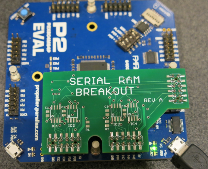
Also using 24MB PSRAM board instead of the onboard memory.
Have to test out the onboard memory next...
Strangely, 24 MB board didn't work so good on basepin 0, but seems fine on basepin 16
That was quick work Rayman. Fingers crossed for your on board PSRAM.
Good job!
Got MegaYume beta 05 running with onboard PSRAM.
Going to try NeoYume next...
That's kind of nice because thing only need 1 chip for that to work...
What's the delay values for the accessory board vs on-board?
beta 05, that's ancient. Better upgrade that. Also, give the
usbnewbranch on either emulator a try for USB Hub support. (Also MegaYume has a bug fix that I did on that branch because I'm lazy)If you're using 16 or 8 bit mode it does use all the chips in the bank.
No luck with NeoYume yet. Thought maybe same memory settings would work, but maybe this clock frequency is higher?
Or, maybe it's because it needs more than one chip and I'm doing something wrong...
No, needs different settings due to different clock speed. Post up your config.
Here's the config.spin2 for MegaYume that worked with onboard PSRAM
Here's the last thing I tried with NeoYume that doesn't work much at all, just garbage on screen with crossed swords game.
Go get versions that aren't super outdated and try those.
And because I realize these aren't posted anywhere highly visible, the links where the newest version lives:
MegaYume master: https://github.com/IRQsome/MegaYume/tree/master
MegaYume new USB driver testing: https://github.com/IRQsome/MegaYume/tree/usbnew
NeoYume master: https://github.com/IRQsome/NeoYume/tree/master
NeoYume new USB driver testing: https://github.com/IRQsome/NeoYume/tree/usbnew
Ok, got latest MegaYume running with attached config.spin2
Also, again had to make this change in megayume_upper.spin2 to account for non-standard uSD pins:
Now to see if can get latest NeoYume to work with onboard PSRAM...
You're using 4 bit mode, you probably want 16 bit mode instead:
Ok, NeoYume now running crossed swords game with PSRAM8 driver and attached config.
Think PSRAM16 not working because have two clock pins for some reason...
Probably have to mod the driver to make that work...