@evanh said:
The weirdest thing ... I can't replicate the mishandled CLK glitches any longer. I've gone back to post #24 and removed the deglitcher code. So now it just simply waits for CS low to start. It works nice and clean.
Must be the tx program working better maybe ... yep, an intentionally inserted CLK glitch during CS high does the job of fooling the rx code when the deglitcher is missing.
Tolerating clock glitches is certainly a nice feature.
What SPI speeds can this run to on a mid-speed P2 ?
I see FT2232H claims 30MHz and CH347 claims 36MHz (master only), so those HS-USB Bridge parts are useful candidates.
Rx smartpin hardware seems fine up to sysclock/3, errors occur at 10% over that. Limited by Nyquist sampling plus some jitter allowance I guess. So it is tight but 100 Mbit/s does work. The inner code loop is good for sysclock/2.
Tx smartpin hardware has a different problem set, if wanting to build by-directional setup. The tx bit-shifter is directly impacted by the Prop2's I/O staging latency. So the clock-data phase relationship has to be managed to achieve SPI looking timing specs as a slave device. It probably won't be completely possible. The software on the master device will likely need to accommodate this limitation.
EDIT: Or maybe not so bad as I'm making out. Smartpins might be good for a lag of four sysclock ticks. That would be manageable on the slave end only I think. I'll need to double check ...
EDIT2: A negative side effect is the tx smartpin will output large stepped tx jitter across sysclock samples. The master will need to be true sync shifter to handle it. And sysclock/3 will be too coarse me thinks. That's two reasons to limit to at least sysclock/4 now.
For tx, I/O staging latency produces a clock-in to data-out phase lag of 3 to 4 (with sampling jitter) sysclock ticks. This gets extended by 1 or 2 ticks by enabling pin registration on each of clock and data pins.
This is substantially better than what the Cogs can do. Another 5 ticks (stages) there. It maybe 4 more stages with the ALU execution time a factor (6 for I/O stages + 2 for instruction execution). The 3 ticks for a smartpin is probably 2 ticks for I/O stages (1 in and 1 out) and 1 tick for the smartpin itself.
I think Chip has stated Cog I/O stages are more on the outgoing than incoming, so it'll be 2 input stages and 4 output stages. Nope, it's just a difference in execution between TESTP and reading INA/INB. There is 3 stages each way using a Cog. From the docs:
[damn, deleted the wrong post Don't even remember what I posted here]
Hmm, it was about tx smartpin being limited to sysclock/6 ...
EDIT5000: Here's a scope capture of the sampling jitter at sysclock/6 data rate when linking data from two clock sources. The blue trace is from the slave Prop2. The other three traces are all from the master. Scope is triggered from the master's falling CS pin (green trace). Both master and slave are outputting the same data pattern.
The blue trace is clocked out on the rising clock (orange trace), it demonstrates the 3 to 4 ticks of lag from the I/O latency and smartpin response. Even if there wasn't any I/O staging registers the same jitter would exist as 1 to 2 ticks of lag because, in the Prop2, the SPI clock is not used to actually clock a real register. It's just another sampled I/O pin.
And a second capture at sysclock/8 data rate. You can see how the phase lag shifts because the latency is still 3 to 4 ticks from the rising clock edge. Sysclock is at 4 MHz for easy capture, in case anyone was wondering why the data rate is so slow.
I think I've got my head around it now. I've spent a few days, on and off over the last week, writing up functional comments for it too:
/*
 *      ____     Mode 0 : CPHA=0  CPOL=0       ____
 *   CS     |_________________________________|
 *             _   _   _   _   _   _   _   _
 *  CLK ______| |_| |_| |_| |_| |_| |_| |_| |______
 *           ___ ___ ___ ___ ___ ___ ___ ___
 * MOSI ----X___X___X___X___X___X___X___X___XXX----
 * MISO       7   6   5   4   3   2   1   0
 *
 *
 *      ____     Mode 3 : CPHA=1  CPOL=1       ____
 *   CS     |_________________________________|
 *      ______   _   _   _   _   _   _   _   ______
 *  CLK       |_| |_| |_| |_| |_| |_| |_| |_|
 *             ___ ___ ___ ___ ___ ___ ___ ___
 * MOSI ----XXX___X___X___X___X___X___X___X___X----
 * MISO         7   6   5   4   3   2   1   0
 *
 *
 * As a minimum, SPI requires just half clock cycle from CS low to first clock
 *      ____ <------>
 *   CS     |________________________ ......
 *                   _______
 *  CLK ____________|       |_______| ......
 *
 * The easy solution is enable the serial smartpin after CS falls:
 *      waitse1    // wait for falling edge
 *      dirh #MOSI    // enable RX smartpin
 * However, this becomes impossible once the SPI clock is faster than the time
 * it takes to enable the smartpin.  Bear in mind that the Prop2's I/O staging
 * latency impacts how quickly software can respond to CS falling.
 * At 10 Mbit/s, there's just 50.0 nanoseconds to both identify CS low then
 * enable the smartpin before missing that first CLK edge.  This is tight for
 * software even at 200 MHz sysclock.  Whereas the smartpin can handle a bit
 * rate of up to sysclock/3.  So, 66 Mbit/s using 200 MHz sysclock.
 *
 * Just to be clear, collecting the wrong number of clock pulses will
 * mangle your data!
 *
 *
 **** THE SOLUTION ****
 *
 * The alternative is to enable the serial smartpin before CS is lowered.  This
 * allows fastest clocking but also creates a problem.  Spurious CLK pulses
 * while CS is high do happen for various reasons.  The most likely one is
 * simply because the SPI master controller has just been initailised and can
 * glitch its pins in the process.
 *
 * So, to achieve reliable smartpin starting conditions, some crafted code is
 * needed.  There's two components, state sequence and pin detects.
 *
 * Pin Detects:
 *    Falling CS:  This is an edge detect, it triggers once per CS cycle.
 *    Spurious CLK:  This uses a combo of CS high and CLK high together.  It's
 * important that CLK is masked when CS is low.  Without checking against CS, a
 * regular fast cycling clock would flood this event, resetting the smartpin
 * over and.over until the clock pulses cease.
 *
 * The pattern event also performs a second critical function over what could
 * be achieved through simple fast cycling on a TESTP.  It catches the tiniest
 * clock glitches that can be missed by software sampling in a tight loop,
 * thereby accurately informing the program of smartpin's condition.
 *
 * The pattern event uses 16 bytes of code to configure it but it surely
 * performs a vital job.
 *
 * State Sequence:
 *    The starting phase consisits of the two branch on event instructions,
 * JPAT/JNSE1, with the smarpin resetter instructions, DIRL/DIRH.  The hardware
 * event of JNSE1 wasn't strictly needed but provided a faster loop not needing
 * any TESTP.  That's worth it by itself.
 *
 * Regarding the inner loop:  The exit state changes are decided using TESTP
 * sampling.  This turned out advantageous over using hardware events.  Both the
 * smartpin's buffer full flag and the CS pin produce a steady state indicator
 * that is good to be sampled.  This in turn allows a cleaner logic decision
 * tree.  The smartpin can raise its byte received flag two sysclock ticks after
 * CS pin rises and still be correctly emptied.
 */
@evanh said:
I think I've got my head around it now. I've spent a few days, on and off over the last week, writing up functional comments for it too:
Impressive work.
I can see upper speed comments in earlier posts, but not commented in the last post's code itself ?
What speeds and rules does the improved code allow ?
How long does CS need to be high between bursts ?
@jmg said:
I can see upper speed comments in earlier posts, but not commented in the last post's code itself ?
What speeds and rules does the improved code allow ?
Yep, those all hold true still. I made a lot of edits previously to get the numbers right at the time. The code hasn't evolved much over the last week. Mostly just me testing it out and trying out poorer alternatives.
@jmg said:
How long does CS need to be high between bursts ?
Undefined. The test code makes no attempt.
There's a lot more to it as well. If there is the usual use of SPI commands then command response latency within the CS low period will be a big question too. That's application dependant and can also be tuned but is never going to be the speed of real hardware.
@evanh said:
I think I've got my head around it now. I've spent a few days, on and off over the last week, writing up functional comments for it too:
/*
 *      ____     Mode 0 : CPHA=0  CPOL=0       ____
 *   CS     |_________________________________|
 *             _   _   _   _   _   _   _   _
 *  CLK ______| |_| |_| |_| |_| |_| |_| |_| |______
 *           ___ ___ ___ ___ ___ ___ ___ ___
 * MOSI ----X___X___X___X___X___X___X___X___XXX----
 * MISO       7   6   5   4   3   2   1   0
 *
 *
 *      ____     Mode 3 : CPHA=1  CPOL=1       ____
 *   CS     |_________________________________|
 *      ______   _   _   _   _   _   _   _   ______
 *  CLK       |_| |_| |_| |_| |_| |_| |_| |_|
 *             ___ ___ ___ ___ ___ ___ ___ ___
 * MOSI ----XXX___X___X___X___X___X___X___X___X----
 * MISO         7   6   5   4   3   2   1   0
 *
 *
 * As a minimum, SPI requires just half clock cycle from CS low to first clock
 *      ____ <------>
 *   CS     |________________________ ......
 *                   _______
 *  CLK ____________|       |_______| ......
 *
 * The easy solution is enable the serial smartpin after CS falls:
 *        waitse1    // wait for falling edge
 *        dirh #MOSI    // enable RX smartpin
 * However, this becomes impossible once the SPI clock is faster than the time
 * it takes to enable the smartpin.  Bear in mind that the Prop2's I/O staging
 * latency impacts how quickly software can respond to CS falling.
 * At 10 Mbit/s, there's just 50.0 nanoseconds to both identify CS low then
 * enable the smartpin before missing that first CLK edge.  This is tight for
 * software even at 200 MHz sysclock.  Whereas the smartpin can handle a bit
 * rate of up to sysclock/3.  So, 66 Mbit/s using 200 MHz sysclock.
 *
 * Just to be clear, collecting the wrong number of clock pulses will
 * mangle your data!
 *
 *
 **** THE SOLUTION ****
 *
 * The alternative is to enable the serial smartpin before CS is lowered.  This
 * allows fastest clocking but also creates a problem.  Spurious CLK pulses
 * while CS is high do happen for various reasons.  The most likely one is
 * simply because the SPI master controller has just been initailised and can
 * glitch its pins in the process.
 *
 * So, to achieve reliable smartpin starting conditions, some crafted code is
 * needed.  There's two components, state sequence and pin detects.
 *
 * Pin Detects:
 *    Falling CS:  This is an edge detect, it triggers once per CS cycle.
 *    Spurious CLK:  This uses a combo of CS high and CLK high together.  It's
 * important that CLK is masked when CS is low.  Without checking against CS, a
 * regular fast cycling clock would flood this event, resetting the smartpin
 * over and.over until the clock pulses cease.
 *
 * The pattern event also performs a second critical function over what could
 * be achieved through simple fast cycling on a TESTP.  It catches the tiniest
 * clock glitches that can be missed by software sampling in a tight loop,
 * thereby accurately informing the program of smartpin's condition.
 *
 * The pattern event uses 16 bytes of code to configure it but it surely
 * performs a vital job.
 *
 * State Sequence:
 *    The starting phase consisits of the two branch on event instructions,
 * JPAT/JNSE1, with the smarpin resetter instructions, DIRL/DIRH.  The hardware
 * event of JNSE1 wasn't strictly needed but provided a faster loop not needing
 * any TESTP.  That's worth it by itself.
 *
 * Regarding the inner loop:  The exit state changes are decided using TESTP
 * sampling.  This turned out advantageous over using hardware events.  Both the
 * smartpin's buffer full flag and the CS pin produce a steady state indicator
 * that is good to be sampled.  This in turn allows a cleaner logic decision
 * tree.  The smartpin can raise its byte received flag two sysclock ticks after
 * CS pin rises and still be correctly emptied.
 */
Hii @evanh ,
Thank you for your suggestions and support.
I have tried your code. I made some minor changes according to our setup. It works well for less buffer data.
Sometimes it's not reading the accurate data when I'm sending the data buffer of 8 bytes at a time. I sent a total of 19200 bytes (8 bytes per chunk) of data from the Rpi to the propeller and I got 19043 bytes. I have set Rpi clk freq = 20Mhz and propeller clk freq = 300Mhz.
I have also tried with 50Bytes to 4Kbytes (Rpi Max Limit is 4Kbytes) of buffer data at a time, but got many mismatched and garbage data. So any idea why spi_shiftin code not working for data more than 8 bytes? Also for 8 bytes its missing data. Please find attached updated code.
@evanh said:
That's a very strange set baud of 300400. Why not the common 230400?
Also, what version of FlexC are you compiling with? You should be using at least version 5.9.17. It fixes a bug with inlined pasm.
Hii @evanh,
By mistake, I've taken this baud rate. It was my mistake. I have tested with a 230400 Baud rate. The result is the same. And yes, I am using the updated FlexC version 5.9.17.
Thank you!
What is the minimum number of pins needed to support SPI Flash, µSD and a third SPI device using shared clock and data pins? Only one of the three enabled at any given time.
SPI clock mode 3 is less error prone than mode 0 when using this wiring.
All the slave devices data out pins are tied together. This fails if any of the slaves drive upon chip select (CS). SPI devices typically leave MISO tri-stated until a reply is due. Eg:
I think there was concern, or evidence, that SD cards aren't so friendly. So the Eval Boards have collision protection resistor on the SD DAT pin. Which limits its bandwidth.
EDIT: Yep, SD in SPI mode drives the DAT (MISO) pin one clock cycle after selected. Amusingly, SD mode doesn't do this.
@TonyB_ said:
What is the minimum number of pins needed to support SPI Flash, µSD and a third SPI device using shared clock and data pins? Only one of the three enabled at any given time.
With or without the collision protection resistor, the Eval Board config could be extended:
SPI clock mode 3 is less error prone than mode 0 when using this wiring.
All the slave devices data out pins are tied together. This fails if any of the slaves drive upon chip select (CS). SPI devices typically leave MISO tri-stated until a reply is due.
Ah, you're planning on using an actual Eval Board then. I just realised that two devices both with resistors on MISO won't work. Can't use both an SD card and the W5500 on the same pins. The master won't see solid high-low levels when selecting either slave.
At least that's assuming I've correctly understood the W5500 is driving its MISO immediately upon CS low.
This should work on an Eval Board, and at high speed for the W5500:
Pin     µSD     Flash   W5500

57      HIGH    HIGH    CS3
58      MISO1+  MISO2   MISO3
59      MOSI1   MOSI2   MOSI3
60      CS1     CLK2    HIGH
61      CLK1    CS2++   CLK3

+       via 240 ohm series resistor
++      if selected by switch
@evanh said:
Ah, you're planning on using an actual Eval Board then. I just realised that two devices both with resistors on MISO won't work. Can't use both an SD card and the W5500 on the same pins. The master won't see solid high-low levels when selecting either slave.
At least that's assuming I've correctly understood the W5500 is driving its MISO immediately upon CS low.
I'm thinking of using Edge plus motherboard at first, then replicating Edge on motherboard later when some pins could be changed, however boot pins are hardwired into P2 ROM. Below is another 4-pin option. Would it work?
µSD and Flash or W5500
Pin     µSD     Flash | W5500

58      MISO1+  MISO2 | MOSI3
59      MOSI1   MOSI2 | MISO3
60      CS1     CLK2  | CLK3
61      CLK1    CS2++ | CS3+++

+       via 240 ohm series resistor
++      if Flash selected by switch
+++     if W5500 selected by jumper
@TonyB_ said:
Below is another 4-pin option. Would it work?
No, the problem is that every time CLK1 is lowered to clock the SD card, it also causes the W5500 chip to drive MISO3, which fights with whatever else is active - MOSI1 in that config above.
You could put a 240 ohm resistor in there though since it is fighting the Prop2 rather than the SD card. ie:
Pin     µSD     Flash | W5500

58      MISO1+  MISO2 | MOSI3
59      MOSI1   MOSI2 | MISO3+
60      CS1     CLK2  | CLK3
61      CLK1    CS2++ | CS3+++

+       via 240 ohm series resistor
++      if Flash selected by switch
+++     if W5500 selected by jumper
Hello @evanh
I'm sending data from Raspberry Pi to P2. Considering Raspberry Pi as master and P2 as slave. It's working properly. Now to send acknowledge from P2 to Raspberry Pi in same code, I need function like shiftout. I have tried several ways but nothing received in Raspberry Pi. Can you please share program or function for data transfer from P2 as a slave?
@evanh said:
The source code doesn't indicate what sort of reply the RPi is expecting.
In Rpi, receive any character of single byte from P2. Then Rpi will send data to P2.
Rpi waits till receive byte (say 249). When 249 received it breaks while loop and continue to send data to P2.
int rx = 0;
while (true) {
    rx = spiRx();
    if (rx == 249)
        break;
}
Txfunc();
In P2 used shift_out() to send byte to Rpi.
int m = 0, x = 0, ret =0;
DIRA |= MISO;
_pinl(CS);
m = P_SYNC_TX | P_OE;
m |= ((CLK - MISO) & 0b111) << 24;
x = 0b1_00000 | (8-1);
_pinstart(MISO, m, x, 0);

char i = 249;
shift_out(MISO, CLK, LSBFIRST, 8, i);
Sorry, been a little sidetracked of late. Need to get back into the grove here ...
Ah, first thing that stands out is SPI is MSBit first. I would expect the RPi will want it this way.
Only AC97 codecs use LSBit first. Which is amusing because signal sampling is exactly where order of significance is most impactful. Typical PC industry - Smile-about-face.


Comments
Tolerating clock glitches is certainly a nice feature.
What SPI speeds can this run to on a mid-speed P2 ?
I see FT2232H claims 30MHz and CH347 claims 36MHz (master only), so those HS-USB Bridge parts are useful candidates.
Rx smartpin hardware seems fine up to sysclock/3, errors occur at 10% over that. Limited by Nyquist sampling plus some jitter allowance I guess. So it is tight but 100 Mbit/s does work. The inner code loop is good for sysclock/2.
Tx smartpin hardware has a different problem set, if wanting to build by-directional setup. The tx bit-shifter is directly impacted by the Prop2's I/O staging latency. So the clock-data phase relationship has to be managed to achieve SPI looking timing specs as a slave device. It probably won't be completely possible. The software on the master device will likely need to accommodate this limitation.
EDIT: Or maybe not so bad as I'm making out. Smartpins might be good for a lag of four sysclock ticks. That would be manageable on the slave end only I think. I'll need to double check ...
EDIT2: A negative side effect is the tx smartpin will output large stepped tx jitter across sysclock samples. The master will need to be true sync shifter to handle it. And sysclock/3 will be too coarse me thinks. That's two reasons to limit to at least sysclock/4 now.
EDIT: [grr, that was just wrong] trying again...
For tx, I/O staging latency produces a clock-in to data-out phase lag of 3 to 4 (with sampling jitter) sysclock ticks. This gets extended by 1 or 2 ticks by enabling pin registration on each of clock and data pins.
This is substantially better than what the Cogs can do. Another 5 ticks (stages) there. It maybe 4 more stages with the ALU execution time a factor (6 for I/O stages + 2 for instruction execution). The 3 ticks for a smartpin is probably 2 ticks for I/O stages (1 in and 1 out) and 1 tick for the smartpin itself.
I think Chip has stated Cog I/O stages are more on the outgoing than incoming, so it'll be 2 input stages and 4 output stages. Nope, it's just a difference in execution between TESTP and reading INA/INB. There is 3 stages each way using a Cog. From the docs:
[damn, deleted the wrong post Don't even remember what I posted here]
Hmm, it was about tx smartpin being limited to sysclock/6 ...
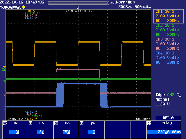
EDIT5000: Here's a scope capture of the sampling jitter at sysclock/6 data rate when linking data from two clock sources. The blue trace is from the slave Prop2. The other three traces are all from the master. Scope is triggered from the master's falling CS pin (green trace). Both master and slave are outputting the same data pattern.
The blue trace is clocked out on the rising clock (orange trace), it demonstrates the 3 to 4 ticks of lag from the I/O latency and smartpin response. Even if there wasn't any I/O staging registers the same jitter would exist as 1 to 2 ticks of lag because, in the Prop2, the SPI clock is not used to actually clock a real register. It's just another sampled I/O pin.
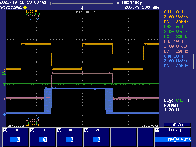
And a second capture at sysclock/8 data rate. You can see how the phase lag shifts because the latency is still 3 to 4 ticks from the rising clock edge. Sysclock is at 4 MHz for easy capture, in case anyone was wondering why the data rate is so slow.
[merged to next post]
I think I've got my head around it now. I've spent a few days, on and off over the last week, writing up functional comments for it too:
Impressive work.
I can see upper speed comments in earlier posts, but not commented in the last post's code itself ?
What speeds and rules does the improved code allow ?
How long does CS need to be high between bursts ?
Yep, those all hold true still. I made a lot of edits previously to get the numbers right at the time. The code hasn't evolved much over the last week. Mostly just me testing it out and trying out poorer alternatives.
Undefined. The test code makes no attempt.
There's a lot more to it as well. If there is the usual use of SPI commands then command response latency within the CS low period will be a big question too. That's application dependant and can also be tuned but is never going to be the speed of real hardware.
Hii @evanh ,
Thank you for your suggestions and support.
I have tried your code. I made some minor changes according to our setup. It works well for less buffer data.
Sometimes it's not reading the accurate data when I'm sending the data buffer of 8 bytes at a time. I sent a total of 19200 bytes (8 bytes per chunk) of data from the Rpi to the propeller and I got 19043 bytes. I have set Rpi clk freq = 20Mhz and propeller clk freq = 300Mhz.
I have also tried with 50Bytes to 4Kbytes (Rpi Max Limit is 4Kbytes) of buffer data at a time, but got many mismatched and garbage data. So any idea why spi_shiftin code not working for data more than 8 bytes? Also for 8 bytes its missing data. Please find attached updated code.
That's a very strange set baud of 300400. Why not the common 230400?
Also, what version of FlexC are you compiling with? You should be using at least version 5.9.17. It fixes a bug with inlined pasm.
Hii @evanh,
By mistake, I've taken this baud rate. It was my mistake. I have tested with a 230400 Baud rate. The result is the same. And yes, I am using the updated FlexC version 5.9.17.
Thank you!
Ah, the compare() function is not moving through the rxdata[] array along with the "count_data".
Here's a revised version of your modified code. I've updated spi_shift_in() to latest revision.
What is the block rate? The printf() code takes time between blocks. I don't know how long, at least a few milliseconds.
This might not be the right place to ask this:
What is the minimum number of pins needed to support SPI Flash, µSD and a third SPI device using shared clock and data pins? Only one of the three enabled at any given time.
With or without the collision protection resistor, the Eval Board config could be extended:
SPI clock mode 3 is less error prone than mode 0 when using this wiring.
All the slave devices data out pins are tied together. This fails if any of the slaves drive upon chip select (CS). SPI devices typically leave MISO tri-stated until a reply is due. Eg:
I think there was concern, or evidence, that SD cards aren't so friendly. So the Eval Boards have collision protection resistor on the SD DAT pin. Which limits its bandwidth.
EDIT: Yep, SD in SPI mode drives the DAT (MISO) pin one clock cycle after selected. Amusingly, SD mode doesn't do this.
Thanks for the info, Evan. Three SPI devices sharing four pins, 58-61, is just what I was hoping for. The third SPI device I have in mind is the WIZnet W5500:
https://docs.wiznet.io/img/products/w5500/w5500_ds_v109e.pdf
Hm, that Wiznet chip appears to drive its MISO pin the moment the chip is selected. Which is even more aggressive than SD cards.
Studying the Eval and Edge schematics again:
Are three devices on pins 58-61 still possible?
With that resistor, yes. You'll need the resistor for the W5500 too. Which limits bit rate of devices using a resistor to about 25 Mbit/s.
What would the pins be for the W5500?
Ah, you're planning on using an actual Eval Board then. I just realised that two devices both with resistors on MISO won't work. Can't use both an SD card and the W5500 on the same pins. The master won't see solid high-low levels when selecting either slave.
At least that's assuming I've correctly understood the W5500 is driving its MISO immediately upon CS low.
This should work on an Eval Board, and at high speed for the W5500:
I'm thinking of using Edge plus motherboard at first, then replicating Edge on motherboard later when some pins could be changed, however boot pins are hardwired into P2 ROM. Below is another 4-pin option. Would it work?
µSD and Flash or W5500
No, the problem is that every time CLK1 is lowered to clock the SD card, it also causes the W5500 chip to drive MISO3, which fights with whatever else is active - MOSI1 in that config above.
You could put a 240 ohm resistor in there though since it is fighting the Prop2 rather than the SD card. ie:
But of course that limits data rate to 25 Mbit/s.
.
Hello @evanh
I'm sending data from Raspberry Pi to P2. Considering Raspberry Pi as master and P2 as slave. It's working properly. Now to send acknowledge from P2 to Raspberry Pi in same code, I need function like shiftout. I have tried several ways but nothing received in Raspberry Pi. Can you please share program or function for data transfer from P2 as a slave?
The source code doesn't indicate what sort of reply the RPi is expecting.
In Rpi, receive any character of single byte from P2. Then Rpi will send data to P2.
Rpi waits till receive byte (say 249). When 249 received it breaks while loop and continue to send data to P2.
int rx = 0; while (true) { rx = spiRx(); if (rx == 249) break; } Txfunc();In P2 used shift_out() to send byte to Rpi.
Sorry, been a little sidetracked of late. Need to get back into the grove here ...
Ah, first thing that stands out is SPI is MSBit first. I would expect the RPi will want it this way.
Only AC97 codecs use LSBit first. Which is amusing because signal sampling is exactly where order of significance is most impactful. Typical PC industry - Smile-about-face.
Okay, I do have a couple of "shiftout" test programs here. I'm not sure if I ever fully tested them though.
Here's one, from October last year, that looks like it just spits out consecutive data from hubRAM as long as CS is low and CLK is toggling.
EDIT: I can see there is a mistake already. There is no return value, yet main() is expecting a byte count.
The second one "shiftout_short" might be more finished. It seems to perform the same but uses a larger 16-bit shifter size.