@rogloh said:
We do already have a USB COG working for keyboards that has recently been reworked and can now also take USB gamepad information (NeoYume uses it). This would be an easy way to use modern USB keyboards and gamepads with a Gigatron emulation.
FTFY: "This would be an easy way to use one modern USB keyboard or gamepad with a Gigatron emulation." ;3
Well it's not that easy I know... but still potentially doable. I was able to get it to work with generic USB gamepad with some mods, and this code you and Marco improved from GarryJ's work is pretty useful.
Yep PS/2 is not too hard to achieve on a P2 though surprisingly I've not seen a PS/2 COG yet (haven't hunted in detail for one though so it might already be available). We used to have a good PS/2 Keyboard SPIN1 COG on the P1 chip. We do already have a USB COG working for keyboards that has recently been reworked and can now also take USB gamepad information (NeoYume uses it). This would be an easy way to use modern USB keyboards and gamepads with a Gigatron emulation. We just need a COG to adapt and drive these inputs into the INPUT port at the correct time.
I think it would need to add ASCII conversion too in order to be compatible with Pluggy. But Pluggy also adds some other I/O features, like being able to accept screen wiggle as an output to write to the internal controller NVRAM for BASIC storage. Of course, it would be better to add the newer expansion method to have a larger pipe for that. It would be nice to take the best of Pluggy reloaded and I/O expander projects. I think one adds assistance with the protocol end but has the slow interface, and the other has a bigger pipe but has to use more driver code in ROM.
If one were to choose to go with a ROM rewrite, you could have the keyboard controller cog write directly to memory, thus timing is less important, hence what I said at the beginning about "lazy writes." I think there is a RAM address to store the result of what comes in. And I imagine one could add more features if that is the case since one could add a cache and use that address as "clothesline memory." So it could accept several keypresses and maybe use them during subsequent pollings. And thus that is back to my original premise of using a stock or maybe a speed-doubled or slightly faster Gigatron. My goal was to have a controller board that is asynchronous from the Gigatron and have an all-in-one solution. Then have it be indirection table aware, I/O commands aware, and perhaps even move the original ports to it for passing commands/data, while it provides its own and works mostly with RAM using snooping as its main DMA strategy for reads. For the writes, do things like lazy writing (wait until /WE and /OE are high and quickly slip in a write), the I/O command protocol with ROM cooperation, and/or spinlocks in ROM. But with the ports being freed up, a custom ROM could support using them for more general I/O or as another way to pass commands.
And with the vCPU only idea I have in mind, it could get some advantages. I am not sure how it multiplies, whether there is a vCPU instruction for that or a syscall for that. Some coders just do their own in vCPU with tables or whatever if they are looking for some speed improvement. But if there is such a thing, the Propeller could do that much faster, even with the overhead. And random numbers would no longer need the native ROM's RAM-scouring method when the P2 has RNGs in every cog and pin.
One video note on the Gigatron is that technically, 6.25 Mhz is a tad slow for VGA. Marcel made up for that by slightly shortening the porches. And that's why the vertical frequency is not quite 60 Hz. In the ROM comments, you can see where Marcel played with different porch values and centered the screen the best he could with a slightly low frequency.
If I could make a dream Gigatron-similar machine with discrete chips, I'd use a 4-stage pipeline and do everything in LUTs. That would allow me to customize the native code some to add full right and left shifters, PRNG, 8/8/16 multiplication, 8/8/8 division. I wouldn't know what to do with 3 delay slots or how to use that for trampolines. As for LUTs, my LUT SRAMs would need to be filled from ROMs on boot somehow. (I don't know if I'd do this, but pre-decoding during boot could save a pipeline stage. So run the System ROM through the CU ROMs and shadow the result.) So have the System ROM and an SRAM, the CU ROM and an SRAM, the user SRAM (and maybe a secondary ALU ROM and SRAM), and the main ALU and an SRAM for it. Yes, that is a lot of ROMs and SRAMs. Plus you'd have pipeline registers between everything. The way I'd interact with RAM would be different than on the Gigatron. Looking at the native code, only reads can be manipulated, never writes. So that explains the "Access" stage out of Fetch, Decode, Access, and Execute. And since User RAM won't be used all the time, I might as well put a table of random numbers and an additional ALU there. Thus, some 16-bit native ops could be possible. Speaking of the user RAM, I might as well use RAM with 20 address bits and 16 data bits. Of course, that adds 2 more control lines and is not exactly compatible with the current implementation. So I could have 2 vCPUs and memory maps. So have one that ignores the upper bytes to keep the 8-bit map (or repurpose it or have another address bit and maybe a mux for that), and one that fully embraces it. And of course, there would need to be more registers to make bit-banging still possible. Now, as for the RAM used for the system RAM and everything else, 10 ns would be the proposed speed. But that complicates things some as that would be SMDs. So I imagine such a contraption could do 75 Mhz. I mentioned more registers, since the way to bit-bang the same resolution at 75 Mhz would be to write to the screen every 12 cycles and let the Out register hold the data during the other 11 cycles. And it would be a complex vCPU to write for sure, since vCPU and video would need to be more intertwined, and similar goes for other I/O. So more registers would be needed to allow for faster context switches. That might require up to 5 new registers to be able to use all the memory and allow for context switches. I mean, a Z register to go with X and Y, 3 registers that duplicate their functionality, and maybe another accumulator. I don't know if that would be too much to chew.
@rogloh said:
By the way I took a look at those vCPU instructions... here's a quick snippet showing roughly the P2 instructions needed in an XBYTE mode to emulate them. For brevity I've neglected the ret at the ends of each instruction handler as this was just a rough sketch only to gauge how easy/hard it might be, and I've left out some stuff I don't yet understand or didn't get to yet...
What will be hard to understand is where branches are placed due to the delay slot and things like trampoline code.
I guess the last argument below is the source (Intel style). I think D is the immediate operand, and it can only be read. So moving from D to Ac makes sense. I am not sure what language that is, but that is not regular assembly. Maybe that is GCL (Gigatron Control Language) which may be a cross between assembly and Perl. Some of these names might be memory locations of virtual registers. I know native Gigatron has no SP register, but vCPU does. Plus I think I see some workaround for a lack of a carry flag. I don't know what the # part does unless that's an offset or something, or if that is a comment.
@PurpleGirl said:
I guess the last argument below is the source (Intel style). I think D is the immediate operand, and it can only be read. So moving from D to Ac makes sense. I am not sure what language that is, but that is not regular assembly. Maybe that is GCL (Gigatron Control Language) which may be a cross between assembly and Perl. Some of these names might be memory locations of virtual registers. I know native Gigatron has no SP register, but vCPU does. Plus I think I see some workaround for a lack of a carry flag. I don't know what the # part does unless that's an offset or something, or if that is a comment.
To spell it out a bit my sample code snippets are written in Propeller2 assembly language (PASM2) or sometimes generically called "PASM" which was the term also used for P1 assembly. In these snippets I've already assumed the existence of P2 register variables called "AC", and "D", and "SP" and "LR" etc which are apparently part of the vCPU architecture. The "#" symbol means a 9 bit constant value as the argument.
In PASM2 the general assembly language syntax is : [label] [execution_condition] operation-mnemonic destination, source [flag_modifiers] ' comment
so
add a, b means register "b" is added to register "a" and the result written back to register "a"
The optional execution_condition prefix let an instruction be executed only when a specific nominated condition is true and skipped otherwise. E.g.: if_c add a, b
means only add register "b" to register "a" if the carry flag C is set, and skip otherwise.
The (mostly) optional flag_modifiers field let you adjust the output flags as a result of the execution of the statement. E.g.: add a, b wc
will write the carry flag a value based on the overflow result of the addition operation.
You can use constants instead of register names in the syntax with the # symbol, typically for source arguments, but sometimes also for destination arguments. E.g.: add a, #3
Adds the immediate value 3 to register "a".
There's a bit more to this than just that but it is a start. I suggest you have a look at the P2 documentation if you want to know more.
@PurpleGirl said:
I think it would need to add ASCII conversion too in order to be compatible with Pluggy. But Pluggy also adds some other I/O features, like being able to accept screen wiggle as an output to write to the internal controller NVRAM for BASIC storage. Of course, it would be better to add the newer expansion method to have a larger pipe for that. It would be nice to take the best of Pluggy reloaded and I/O expander projects. I think one adds assistance with the protocol end but has the slow interface, and the other has a bigger pipe but has to use more driver code in ROM.
If one were to choose to go with a ROM rewrite, you could have the keyboard controller cog write directly to memory, thus timing is less important, hence what I said at the beginning about "lazy writes." I think there is a RAM address to store the result of what comes in. And I imagine one could add more features if that is the case since one could add a cache and use that address as "clothesline memory." So it could accept several keypresses and maybe use them during subsequent pollings. And thus that is back to my original premise of using a stock or maybe a speed-doubled or slightly faster Gigatron. My goal was to have a controller board that is asynchronous from the Gigatron and have an all-in-one solution. Then have it be indirection table aware, I/O commands aware, and perhaps even move the original ports to it for passing commands/data, while it provides its own and works mostly with RAM using snooping as its main DMA strategy for reads. For the writes, do things like lazy writing (wait until /WE and /OE are high and quickly slip in a write), the I/O command protocol with ROM cooperation, and/or spinlocks in ROM. But with the ports being freed up, a custom ROM could support using them for more general I/O or as another way to pass commands.
And with the vCPU only idea I have in mind, it could get some advantages. I am not sure how it multiplies, whether there is a vCPU instruction for that or a syscall for that. Some coders just do their own in vCPU with tables or whatever if they are looking for some speed improvement. But if there is such a thing, the Propeller could do that much faster, even with the overhead. And random numbers would no longer need the native ROM's RAM-scouring method when the P2 has RNGs in every cog and pin.
One video note on the Gigatron is that technically, 6.25 Mhz is a tad slow for VGA. Marcel made up for that by slightly shortening the porches. And that's why the vertical frequency is not quite 60 Hz. In the ROM comments, you can see where Marcel played with different porch values and centered the screen the best he could with a slightly low frequency.
If I could make a dream Gigatron-similar machine with discrete chips, I'd use a 4-stage pipeline and do everything in LUTs. That would allow me to customize the native code some to add full right and left shifters, PRNG, 8/8/16 multiplication, 8/8/8 division. I wouldn't know what to do with 3 delay slots or how to use that for trampolines. As for LUTs, my LUT SRAMs would need to be filled from ROMs on boot somehow. (I don't know if I'd do this, but pre-decoding during boot could save a pipeline stage. So run the System ROM through the CU ROMs and shadow the result.) So have the System ROM and an SRAM, the CU ROM and an SRAM, the user SRAM (and maybe a secondary ALU ROM and SRAM), and the main ALU and an SRAM for it. Yes, that is a lot of ROMs and SRAMs. Plus you'd have pipeline registers between everything. The way I'd interact with RAM would be different than on the Gigatron. Looking at the native code, only reads can be manipulated, never writes. So that explains the "Access" stage out of Fetch, Decode, Access, and Execute. And since User RAM won't be used all the time, I might as well put a table of random numbers and an additional ALU there. Thus, some 16-bit native ops could be possible. Speaking of the user RAM, I might as well use RAM with 20 address bits and 16 data bits. Of course, that adds 2 more control lines and is not exactly compatible with the current implementation. So I could have 2 vCPUs and memory maps. So have one that ignores the upper bytes to keep the 8-bit map (or repurpose it or have another address bit and maybe a mux for that), and one that fully embraces it. And of course, there would need to be more registers to make bit-banging still possible. Now, as for the RAM used for the system RAM and everything else, 10 ns would be the proposed speed. But that complicates things some as that would be SMDs. So I imagine such a contraption could do 75 Mhz. I mentioned more registers, since the way to bit-bang the same resolution at 75 Mhz would be to write to the screen every 12 cycles and let the Out register hold the data during the other 11 cycles. And it would be a complex vCPU to write for sure, since vCPU and video would need to be more intertwined, and similar goes for other I/O. So more registers would be needed to allow for faster context switches. That might require up to 5 new registers to be able to use all the memory and allow for context switches. I mean, a Z register to go with X and Y, 3 registers that duplicate their functionality, and maybe another accumulator. I don't know if that would be too much to chew.
You have plenty of ideas. Mostly they extend/diverge from the original Gigatron HW. The P2 is a very capable system and could certainly do much of what you'd like to try out. It is somewhat fondly termed the "Amiga of microcontrollers", if you are old enough like me to remember what the Amiga was. I'd recommend starting to dig right into the P2 architecture and tools and start experimenting with your ideas. You might start to find you rapidly move beyond the whole Gigatron thing and build what you dream of in a native Propeller environment and language for the highest performance possible. Have a go!
First brief sanity test looks good...I'm outputting a clock from the Gigatron instruction emulator that toggles each time an instruction gets executed and a video byte is sent on one output pin. In a second COG I am toggling another clock pin at the system clock rate divided by 52 cycles. This is running much slower than normal so I can view it, but it will perfectly scale with frequency. These two pin's phase difference should remain stable if the instructions are being executed at the correct rate and the FIFO is not stealing cycles from the reads and writes. I've captured these outputs on my logic analyzer but a proper oscilloscope triggering on a pulse width exceeding a certain value is probably a better way to view it and I might set that up as well. This is just executing garbage from HUB RAM, not a real program, so it's not a proper test yet. I might also use a third COG to try to monitor for any variation in pulse width and drive another pin if that ever happens too, making it easier to detect.
You have plenty of ideas. Mostly they extend/diverge from the original Gigatron HW. The P2 is a very capable system and could certainly do much of what you'd like to try out. It is somewhat fondly termed the "Amiga of microcontrollers", if you are old enough like me to remember what the Amiga was. I'd recommend starting to dig right into the P2 architecture and tools and start experimenting with your ideas. You might start to find you rapidly move beyond the whole Gigatron thing and build what you dream of in a native Propeller environment and language for the highest performance possible. Have a go!
Well, I don't know if my 75 Mhz, 4-stage, Gigatron similar would be worthwhile to do. I mean, this would be using SMDs and mostly memory of one type or another. The problem would be the expense and availability. Good luck finding memory right now, and particularly ROMs. NVRAM is a little more available.
I'd use SRAMs as LUTs because I don't know how to make the circuits involved, and because of the ease of being able to replace instructions and math operations. I mean, for a CU LUT, you'd feed the opcode into the address lines and get the control signal matrix out of the data lines. That may take 2-3 of the 16-bit ROMs. The Gigatron native code has a lot of useless instructions, and all native code to date uses the lowest values that can do a job. So only the first NOP is used and not the other 11 that can do that. So with a LUT ROM/RAM combo, you can arbitrarily repurpose redundant or useless instructions. So more registers, full shift functions, random numbers, multiplication, and division would be available.
But how would I deal with a 75 Mhz bus if I wanted I/O help from another device? The ISA bus, for instance, ran at 4.77 to 8 Mhz. The original PCI could do up the 33 Mhz. And being able to respond within 15 ns or less would be a challenge for a P2, even at max. That would be more of a job for an FPGA since an I/O controller could be deeply pipelined and have many parallel processes. With the snooper idea, instead of a broad-range snooper, one would have time to narrow the search to specific ranges if multiple snoopers were used. But, that said, with 75 Mhz for a simple design, bit-banging would be more feasible. And in true 16-bit mode as opposed to 8-16 that the Gigatron vCPU emulates, things could go faster. Up to 150 Mips for native code isn't bad. But one would practically never achieve that with such an arrangement.
I know I could have fun with a P2, but I'd then want a design that integrates more with the P2 and uses its abilities, even if it uses a virtual ISA. I've thought about the feasibility of adding a 16-bit parallel, async SRAM, but that will take up 40 GPIO lines. (20 address bits, 16 data bits, 4 control lines). That leaves 24 and then you have the pre-determined pins. And one might want to add a /halt line to allow for DMA. Some do use such an approach and use multiple P2s. Maybe not the most efficient way to do it, but faster than the approach of the Hydra that used serial lines for everything.
And are there easy ways to convert virtual instructions to code on the P2? For instance, the Gigatron does it by jumping to ROM locations that are what is in the RAM location of the vCPU instruction. Of course, that is why the instruction map is only about 1/3 full, to leave room for branches, thus making many addresses unavailable to work as instructions. Even newer BASIC compilers have the Switch command that lets you jump based on a list rather than polling for every condition.
I like some of the ideas behind the Foenix Computer. In the early generations, Stefany used FPGAs for most things. If I were her, I'd have likely used an FPGA for the '816 CPU as well. That would be faster than Bill Mensch's 14 Mhz '816, and you could then remove multiplexing to avoid limiting the board speed. Oh, and you could mod it to default to '816 mode instead of the 6502 CPU mode to simplify an 816-only machine. But she used a stock chip for that. She did refuse to make her FPGA source open and I get her reasons. The idea is to impose limits to provide compatibility, and if others mod her code for their chips, they'd remove such limits or create confusion. So it is easier to give chips names and control the tech. If others want to reverse engineer them, and make something a little different, then they could do that. So she wanted to make folks work for what they want a bit. At some point, she decided to quit making them because everyone was griping about features they wanted, and few were using the features she provided such as a sound system that people would have been willing to kill for in the '80s. I mean, it had 2 SID clones, emulated two Yamaha chips, had a sound management and coprocessor chip, and used a DAC that was really a bit of overkill. And folks were talking about porting Linux to it, writing their own OS, etc., and never mentioned the sound hardware. But then, she started making them again and offered 3rd-party CPUs on modules. So you can put a 68xxx chip or a 486 DX on it too. I wonder how well a port of DOOM would work on that.
@rogloh said:
First brief sanity test looks good...I'm outputting a clock from the Gigatron instruction emulator that toggles each time an instruction gets executed and a video byte is sent on one output pin. In a second COG I am toggling another clock pin at the system clock rate divided by 52 cycles. This is running much slower than normal so I can view it, but it will perfectly scale with frequency. These two pin's phase difference should remain stable if the instructions are being executed at the correct rate and the FIFO is not stealing cycles from the reads and writes. I've captured these outputs on my logic analyzer but a proper oscilloscope triggering on a pulse width exceeding a certain value is probably a better way to view it and I might set that up as well. This is just executing garbage from HUB RAM, not a real program, so it's not a proper test yet. I might also use a third COG to try to monitor for any variation in pulse width and drive another pin if that ever happens too, making it easier to detect.
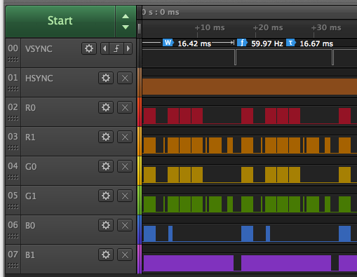
Did some simple sanity opcode tests (not exhaustive), and the emulator seems okay, so I just loaded the Gigatron v4 ROM to see what would happen, thinking not much. Suprisingly I noticed it was pulsing the LEDs on the board in a Larson scanner style output, then I probed its video output port.
Looky what I see on my Logic Analyzer capturing its parallel/EGA port output...
Now I just have to get the VGA part working to see this on screen (or make up a simple DAC board).
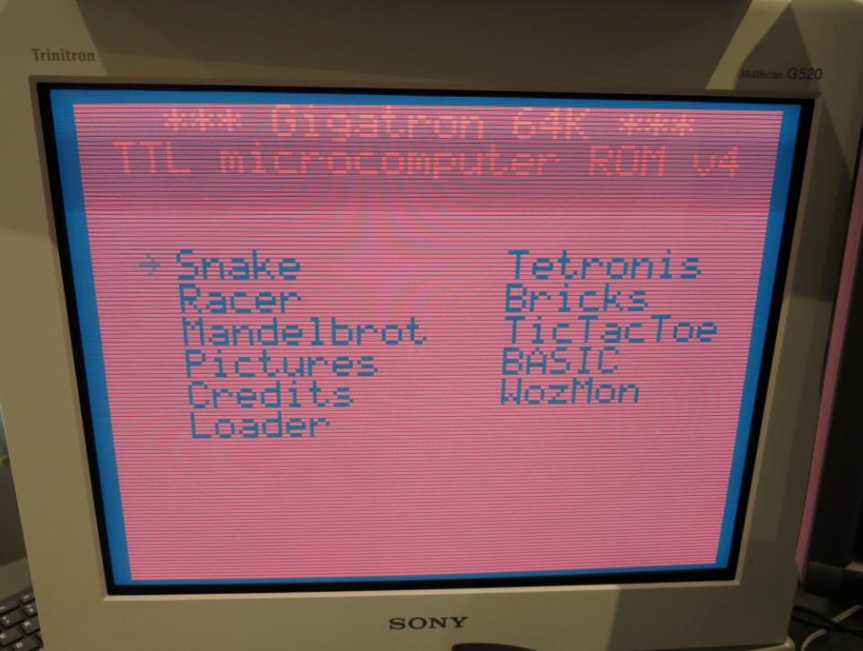
Forgot to put the COGID into the DAC config longs for the VGA pins. Fixed that and now I see this on the VGA port. Sync appears solid. Not sure if the colours are correct or not being all in red. But happy to see this and I can probably move onto the IO stuff.
Here's the latest code with fixes etc for anyone playing along.
@rogloh said:
Forgot to put the COGID into the DAC config longs for the VGA pins. Fixed that and now I see this on the VGA port. Sync appears solid. Not sure if the colours are correct or not being all in red. But happy to see this and I can probably move onto the IO stuff.
Yeah, the colors are off. On that screen, you could get yellow text and a blue background.
Now that looks better. Some of the stock ones do blue, white, and yellow like yours. Others do blue and yellow. I imagine the ROM version has something to do with that.
If you want to work on the I/O, you might do better to use ROM 5A or the DevROM. That adds things to use some of the expander boards some have made. That uses the "undefined" memory instructions that assert both /WE and /OE. That is not a valid control state for the memory. Some ignores it or only writes, but some comingle what is on the bus with what is already there. And current add-on cards exploit this and take the RAM off the bus and do whatever is passed to it. I am unsure how things are passed. I think I read somewhere that it is the address bus that does the command passing. But really, I'd go to the forum at Gigatron.IO and read what the techier folks have said.
Yeah I think I figured it all out and it's the address bus that passes the data in this case. I've emulated the updated IO expansion board with this mapping of bits below that I discovered in those Gigatron forums. It gives you control of 4 SPI devices and 4 RAM banks (128KB). I noticed this older v4 ROM only reported 64kB so it probably didn't detect this type of expansion RAM banking and I thought I might have a bug somewhere there, but if the ROM needs to be newer that could explain things. I can try the later ROM.
' EXPANSION IO MAPPING OF ADDRESS BITS IN CTRL WRITE
' A15 - SPI MOSI OUTPUT
' A7 - RAM BANK
' A6 - RAM BANK
' A5:A2 - SPI CS OUTPUTS
' A1 - UNUSED
' A0 - SPI CLK & RAM/IO READ SELECT BIT
@rogloh said:
Yeah I think I figured it all out and it's the address bus that passes the data in this case. I've emulated the updated IO expansion board with this mapping of bits below that I discovered in those Gigatron forums. It gives you control of 4 SPI devices and 4 RAM banks (128KB). I noticed this older v4 ROM only reported 64kB so it probably didn't detect this type of expansion RAM banking and I thought I might have a bug somewhere there, but if the ROM needs to be newer that could explain things. I can try the later ROM.
I thought 256 was more the max if 64K banks were allowed. The stock Gigatron only provides 32K, but some have modded the socket and used the breakout for A15, and theirs report 64K. Or course, that has been debated in the forum, whether banks should be 32K or 64K.
And with one of the expansion boards, they added 512K. They may have used unused lines or repurposed some. Not everyone would want 4 SPI buses, for instance, and those can be repurposed as additional bank selectors.
One board went as far as to add a Z register, meaning it was physically possible to use memory with 20-24 address bits. They customized the control protocol a bit to let the Gigatron set this extra index register.
Another thing folks do is to repurpose 2 of the lights for adding sound resolution. I am not 100% sure, but they put the extra bits on the bottom since the low nibble is sound and the upper nibble of X-Out is Blinkenlights. That helps the sound some due to the fact that the internal samples are 6-bits. Using 8-bits would help more, but not as much since the samples are 6 bits, and that would help more with mixing channels since you'd lose less aggregated resolution. With the current Gigatron, that's a hard thing to decide since that can break compatibility the same. If I were interested in breaking compatibility, I'd use all the bits in order. With stock programs, that would work since you'd mod the ROM to allow that and remove the cap. But then, the software could be an issue. For instance, PucMon edits 1-2 of the sample tables to add custom sounds. A workaround I've considered for a controller would be to let stock sounds play at whatever resolution you want since you could use your own sound tables. But watch to see if any software changes those so the controller can use the modified samples. So then you'd get better sound and a fallback mode for using custom sounds. But of course, some like more gritty sounds with the occasional artifacts (quantization noise).
@rogloh said:
Newer v5a ROM does report 128kB (and a couple of different programs).
That is neat, though some have reported bugs in ROM 5A. I don't remember reading what they are. But that is understandable. Marcel knew he didn't have long, so he sorta rushed that one. So users like AT67 have written a newer one that fixes the bugs and might support newer boards.
We can certainly support 256kB if banks are actually 64kB, not 32kB in size. 512kB RAM is too much for the P2 to fit everything into HUB RAM including the 128kB ROM image as well. You could use external memory to expand memory further but not with a fully synced 6.25MHz emulation. Not enough time to get a random access result in one cycle. That external memory would be far better used as a large video frame buffer with mailbox control to transfer pixel data in and out from Gigatron RAM space which the P2 can share from other COGs.
If this works out, and I think it most probably will now based on what I'm seeing, people can always modify extend what I put together to support other IO features. You could have further IO COGs doing other things too in parallel or replacing the one I wrote which currently has to do VGA VIDEO+sync/AUDIO/LED outputs and serialize the input data. It's really tightly packed in to fit in with 325MHz operation. Amazingly the P2 can (just) handle this, right down to the clock cycle. Hopefully we won't encounter weird FIFO slowdowns that could corrupt video output...so far I've not seen any but it's early days.
@rogloh said:
We can certainly support 256kB if banks are actually 64kB, not 32kB in size. 512kB RAM is too much for the P2 to fit everything into HUB RAM including the 128kB ROM image as well. You could use external memory to expand memory further but not with a fully synced 6.25MHz emulation. Not enough time to get a random access result in one cycle. That external memory would be far better used as a large video frame buffer with mailbox control to transfer pixel data in and out from Gigatron RAM space which the P2 can share from other COGs.
If this works out, and I think it most probably will now based on what I'm seeing, people can always modify extend what I put together to support other IO features. You could have further IO COGs doing other things too in parallel or replacing the one I wrote which currently has to do VGA VIDEO+sync/AUDIO/LED outputs and serialize the input data. It's really tightly packed in to fit in with 325MHz operation. Amazingly the P2 can (just) handle this, right down to the clock cycle. Hopefully we won't encounter weird FIFO slowdowns that could corrupt video output...so far I've not seen any but it's early days.
Yeah, I understand the hub RAM limitations. And serial memory is possible to add, but as you said, that would slow things down. And we know parallel SRAM would take up too many pins. That would take up 29-30 pins (19-20 address bits, 2 control lines, and 8 data lines).
I'm glad you made this. It makes a nice testbed for testing other possible features. Like with my idea for splitting the video, while it sounds nice, there is no telling what software race conditions that this could introduce. So this would be a way to test this without making/using other hardware. Similar goes with sound. With more processing time from a modified ROM that provides no video support, values could get overwritten before they are used. You wouldn't have hardware races because of the way the hub works, but code races are another issue. I've thought about having a halt line, thus if one splits out the video, there would be a way to gate things and keep performance at stock levels.
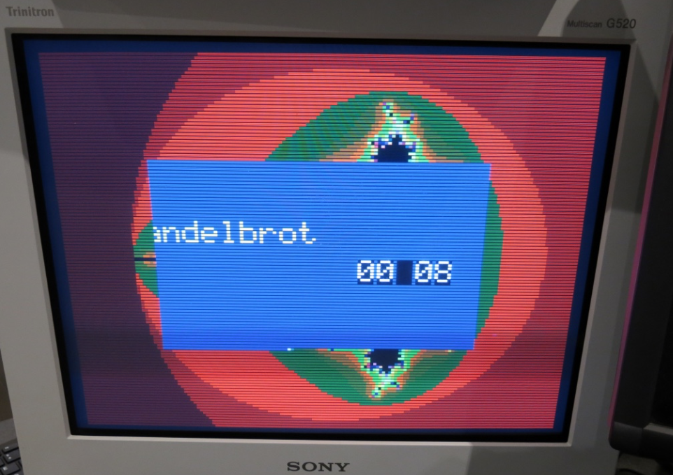
Just hooked up a SNES style game controller and got the input working in the game controller mode (not serial port data quite yet). I just ran the controller I had at 3.3V (likely a CMOS 4021 etc) and it worked directly wired to the P2 pins without any resistor needed. I could run the snake and car racing game with it. Works fine. Select seems to cycle the actively rendered scan lines per pixel and holding Start down resets the system as expected. No evidence of sync corruption so far, very solid with the P2 @ 325MHz/6.25MHz Gigatron emulation. That Mandelbrot set is a pretty slow to render at this speed though. I'm watching it crawl along until I increase the CPU time by dropping the actively drawn scan lines.
Be nice to have the actual mating connector for the game controller. Only wire I had that fits inside it was some thick enameled stuff I had lying about and took ages to scrape it off. Am loathed to cut the connector off but I might.
@rogloh said:
No evidence of sync corruption so far, very solid with the P2 @ 325MHz/6.25MHz Gigatron emulation.
Good work, Roger. I have done more testing and I understand full FIFO loading now. Partial FIFO filling to be investigated.
RDFAST with wait takes 10-17 cycles, one more than RDLONG with the extra cycle at the start. RDBYTE, RDWORD & RDLONG have a fixed pre-read time of 3 cycles, then a variable read time of 1-8 cycles depending on egg beater hub RAM slice, then a fixed post-read time of 5 cycles, making a total of 9-16 assuming no long crossing that would add an extra cycle. WRBYTE, WRWORD, WRLONG & WMLONG have a fixed pre-write time of 3 cycles and a variable write time of 0-7 cycles, again assuming no long crossing.
The FIFO depth of 19 means 18 longs must be read in 18 cycles immediately after the first long. A random hub read or write will be delayed after RDFAST if the random read or write slice coincides with any of these 18 FIFO read slices. The post-read time of 5 cycles for RDFAST and pre-read or pre-write time of 3 cycles for the hub access add up to 8 cycles, which leaves a minimum time of 10 cycles between end of RDFAST with wait and start of random read/write to avoid the latter being delayed.
N.B. The 10 cycle minimum is increased by one cycle every time RFxxxx consumes a long when the FIFO is still filling. A long is consumed by every RFLONG, or by RFWORD that starts at bytes 2 or 3, or by RFBYTE at byte 3.
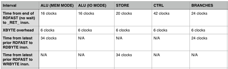
Well that's useful information @TonyB_. Here's the timing I think we have between the relevant instructions in my code.
Also audio is working now. It's hardly the best sounding stuff, being 4bit audio, but it is what it is and can be output over the A/V breakout board now.
I still have to check through the SPI pin IO and try to get the serial input working. But the basics with the game controller interface, that is video+audio+leds+game port is apparently all working so far. It does need to build with DEBUG mode in FlexSpin (the -gbrk option) for some reason and I'm still figuring out why it fails to start up properly without that. Might be PLL related as this was pure PASM without SPIN2, or it could need a delay after COG startup to sync the two correctly. So if you build this just use the -gbrk option.
RLs-MacBook-Pro:gigatron roger$ flexspin -gbrk gigatron.spin2
Propeller Spin/PASM Compiler 'FlexSpin' (c) 2011-2021 Total Spectrum Software Inc.
Version 5.9.3-beta-v5.9.2-33-g35412c83 Compiled on: Sep 26 2021
gigatron.spin2
gigatron.spin2
Done.
Program size is 268904 bytes
RLs-MacBook-Pro:gigatron roger$ loadp2 -t gigatron.binary
Could not find a P2
RLs-MacBook-Pro:gigatron roger$ loadp2 -t gigatron.binary
( Entering terminal mode. Press Ctrl-] or Ctrl-Z to exit. )
Cog0 INIT $0000_0000 $0000_0000 load
Cog1 INIT $0000_0380 $0000_0000 load
Latest code is attached - and it's moved to beta status now since it's essentially usable for all the basic Gigatron functions (with a game controller anyway).
@TonyB_ said:
The FIFO depth of 19 means 18 longs must be read in 18 cycles immediately after the first long. A random hub read or write will be delayed after RDFAST if the random read or write slice coincides with any of these 18 FIFO read slices. The post-read time of 5 cycles for RDFAST and pre-read or pre-write time of 3 cycles for the hub access add up to 8 cycles, which leaves a minimum time of 10 cycles between end of RDFAST and start of hub read/write to avoid the latter being delayed.
For a non-blocking RDFAST, the max post-RDFAST ticks needed will be 17 (start filling) + 18 (fill complete) - 2 (non-blocking execution) = 33 ticks.
Yeah I am hoping we are mostly okay except that branch case. Looking at the branch code I think I can possibly rearrange it a bit to buy a few more clocks before we need to do the RDBYTE. The main thing is to not read from the FIFO before it is ready, that will lock up the system. If the other RDBYTE or WRBYTE cycles happen to be delayed a bit, it might corrupt video temporarily with an extra pixel on a line, but it may not be too noticeable unless it happens a lot. I just want to make sure it doesn't hang or something.
@rogloh said:
I still have to check through the SPI pin IO and try to get the serial input working. But the basics with the game controller interface, that is video+audio+leds+game port is apparently all working so far. It does need to build with DEBUG mode in FlexSpin (the -gbrk option) for some reason and I'm still figuring out why it fails to start up properly without that. Might be PLL related as this was pure PASM without SPIN2, or it could need a delay after COG startup to sync the two correctly. So if you build this just use the -gbrk option.
@rogloh said:
Why would the FIFO fill waste 17 clocks before it even starts reading???
In the worst case, it needs to finish writing up to 8 or so longs and then wait a whole rotation before it reaches the slice it wants to start reading at.
BTW, FIFO writes are unlikely to be buffer delayed in the FIFO. Testing has proven they are always written to hubRAM ASAP, to the detriment of throughput.
Thinking about it a little more, that 33 ticks may not be right either. The 5 post-hubRAM stages won't matter since they are just like a pipeline so don't need to be emptied first. Then, 28 ticks after a non-blocking RDFAST should be clear.


Comments
Well it's not that easy I know... but still potentially doable. I was able to get it to work with generic USB gamepad with some mods, and this code you and Marco improved from GarryJ's work is pretty useful.
I think it would need to add ASCII conversion too in order to be compatible with Pluggy. But Pluggy also adds some other I/O features, like being able to accept screen wiggle as an output to write to the internal controller NVRAM for BASIC storage. Of course, it would be better to add the newer expansion method to have a larger pipe for that. It would be nice to take the best of Pluggy reloaded and I/O expander projects. I think one adds assistance with the protocol end but has the slow interface, and the other has a bigger pipe but has to use more driver code in ROM.
If one were to choose to go with a ROM rewrite, you could have the keyboard controller cog write directly to memory, thus timing is less important, hence what I said at the beginning about "lazy writes." I think there is a RAM address to store the result of what comes in. And I imagine one could add more features if that is the case since one could add a cache and use that address as "clothesline memory." So it could accept several keypresses and maybe use them during subsequent pollings. And thus that is back to my original premise of using a stock or maybe a speed-doubled or slightly faster Gigatron. My goal was to have a controller board that is asynchronous from the Gigatron and have an all-in-one solution. Then have it be indirection table aware, I/O commands aware, and perhaps even move the original ports to it for passing commands/data, while it provides its own and works mostly with RAM using snooping as its main DMA strategy for reads. For the writes, do things like lazy writing (wait until /WE and /OE are high and quickly slip in a write), the I/O command protocol with ROM cooperation, and/or spinlocks in ROM. But with the ports being freed up, a custom ROM could support using them for more general I/O or as another way to pass commands.
And with the vCPU only idea I have in mind, it could get some advantages. I am not sure how it multiplies, whether there is a vCPU instruction for that or a syscall for that. Some coders just do their own in vCPU with tables or whatever if they are looking for some speed improvement. But if there is such a thing, the Propeller could do that much faster, even with the overhead. And random numbers would no longer need the native ROM's RAM-scouring method when the P2 has RNGs in every cog and pin.
One video note on the Gigatron is that technically, 6.25 Mhz is a tad slow for VGA. Marcel made up for that by slightly shortening the porches. And that's why the vertical frequency is not quite 60 Hz. In the ROM comments, you can see where Marcel played with different porch values and centered the screen the best he could with a slightly low frequency.
If I could make a dream Gigatron-similar machine with discrete chips, I'd use a 4-stage pipeline and do everything in LUTs. That would allow me to customize the native code some to add full right and left shifters, PRNG, 8/8/16 multiplication, 8/8/8 division. I wouldn't know what to do with 3 delay slots or how to use that for trampolines. As for LUTs, my LUT SRAMs would need to be filled from ROMs on boot somehow. (I don't know if I'd do this, but pre-decoding during boot could save a pipeline stage. So run the System ROM through the CU ROMs and shadow the result.) So have the System ROM and an SRAM, the CU ROM and an SRAM, the user SRAM (and maybe a secondary ALU ROM and SRAM), and the main ALU and an SRAM for it. Yes, that is a lot of ROMs and SRAMs. Plus you'd have pipeline registers between everything. The way I'd interact with RAM would be different than on the Gigatron. Looking at the native code, only reads can be manipulated, never writes. So that explains the "Access" stage out of Fetch, Decode, Access, and Execute. And since User RAM won't be used all the time, I might as well put a table of random numbers and an additional ALU there. Thus, some 16-bit native ops could be possible. Speaking of the user RAM, I might as well use RAM with 20 address bits and 16 data bits. Of course, that adds 2 more control lines and is not exactly compatible with the current implementation. So I could have 2 vCPUs and memory maps. So have one that ignores the upper bytes to keep the 8-bit map (or repurpose it or have another address bit and maybe a mux for that), and one that fully embraces it. And of course, there would need to be more registers to make bit-banging still possible. Now, as for the RAM used for the system RAM and everything else, 10 ns would be the proposed speed. But that complicates things some as that would be SMDs. So I imagine such a contraption could do 75 Mhz. I mentioned more registers, since the way to bit-bang the same resolution at 75 Mhz would be to write to the screen every 12 cycles and let the Out register hold the data during the other 11 cycles. And it would be a complex vCPU to write for sure, since vCPU and video would need to be more intertwined, and similar goes for other I/O. So more registers would be needed to allow for faster context switches. That might require up to 5 new registers to be able to use all the memory and allow for context switches. I mean, a Z register to go with X and Y, 3 registers that duplicate their functionality, and maybe another accumulator. I don't know if that would be too much to chew.
What will be hard to understand is where branches are placed due to the delay slot and things like trampoline code.
I guess the last argument below is the source (Intel style). I think D is the immediate operand, and it can only be read. So moving from D to Ac makes sense. I am not sure what language that is, but that is not regular assembly. Maybe that is GCL (Gigatron Control Language) which may be a cross between assembly and Perl. Some of these names might be memory locations of virtual registers. I know native Gigatron has no SP register, but vCPU does. Plus I think I see some workaround for a lack of a carry flag. I don't know what the # part does unless that's an offset or something, or if that is a comment.
To spell it out a bit my sample code snippets are written in Propeller2 assembly language (PASM2) or sometimes generically called "PASM" which was the term also used for P1 assembly. In these snippets I've already assumed the existence of P2 register variables called "AC", and "D", and "SP" and "LR" etc which are apparently part of the vCPU architecture. The "#" symbol means a 9 bit constant value as the argument.
In PASM2 the general assembly language syntax is :
[label] [execution_condition] operation-mnemonic destination, source [flag_modifiers] ' commentso
add a, b means register "b" is added to register "a" and the result written back to register "a"
The optional execution_condition prefix let an instruction be executed only when a specific nominated condition is true and skipped otherwise. E.g.:
if_c add a, bmeans only add register "b" to register "a" if the carry flag C is set, and skip otherwise.
The (mostly) optional flag_modifiers field let you adjust the output flags as a result of the execution of the statement. E.g.:
add a, b wcwill write the carry flag a value based on the overflow result of the addition operation.
You can use constants instead of register names in the syntax with the # symbol, typically for source arguments, but sometimes also for destination arguments. E.g.:
add a, #3Adds the immediate value 3 to register "a".
There's a bit more to this than just that but it is a start. I suggest you have a look at the P2 documentation if you want to know more.
You have plenty of ideas. Mostly they extend/diverge from the original Gigatron HW. The P2 is a very capable system and could certainly do much of what you'd like to try out. It is somewhat fondly termed the "Amiga of microcontrollers", if you are old enough like me to remember what the Amiga was. I'd recommend starting to dig right into the P2 architecture and tools and start experimenting with your ideas. You might start to find you rapidly move beyond the whole Gigatron thing and build what you dream of in a native Propeller environment and language for the highest performance possible. Have a go!
First brief sanity test looks good...I'm outputting a clock from the Gigatron instruction emulator that toggles each time an instruction gets executed and a video byte is sent on one output pin. In a second COG I am toggling another clock pin at the system clock rate divided by 52 cycles. This is running much slower than normal so I can view it, but it will perfectly scale with frequency. These two pin's phase difference should remain stable if the instructions are being executed at the correct rate and the FIFO is not stealing cycles from the reads and writes. I've captured these outputs on my logic analyzer but a proper oscilloscope triggering on a pulse width exceeding a certain value is probably a better way to view it and I might set that up as well. This is just executing garbage from HUB RAM, not a real program, so it's not a proper test yet. I might also use a third COG to try to monitor for any variation in pulse width and drive another pin if that ever happens too, making it easier to detect.
Well, I don't know if my 75 Mhz, 4-stage, Gigatron similar would be worthwhile to do. I mean, this would be using SMDs and mostly memory of one type or another. The problem would be the expense and availability. Good luck finding memory right now, and particularly ROMs. NVRAM is a little more available.
I'd use SRAMs as LUTs because I don't know how to make the circuits involved, and because of the ease of being able to replace instructions and math operations. I mean, for a CU LUT, you'd feed the opcode into the address lines and get the control signal matrix out of the data lines. That may take 2-3 of the 16-bit ROMs. The Gigatron native code has a lot of useless instructions, and all native code to date uses the lowest values that can do a job. So only the first NOP is used and not the other 11 that can do that. So with a LUT ROM/RAM combo, you can arbitrarily repurpose redundant or useless instructions. So more registers, full shift functions, random numbers, multiplication, and division would be available.
But how would I deal with a 75 Mhz bus if I wanted I/O help from another device? The ISA bus, for instance, ran at 4.77 to 8 Mhz. The original PCI could do up the 33 Mhz. And being able to respond within 15 ns or less would be a challenge for a P2, even at max. That would be more of a job for an FPGA since an I/O controller could be deeply pipelined and have many parallel processes. With the snooper idea, instead of a broad-range snooper, one would have time to narrow the search to specific ranges if multiple snoopers were used. But, that said, with 75 Mhz for a simple design, bit-banging would be more feasible. And in true 16-bit mode as opposed to 8-16 that the Gigatron vCPU emulates, things could go faster. Up to 150 Mips for native code isn't bad. But one would practically never achieve that with such an arrangement.
I know I could have fun with a P2, but I'd then want a design that integrates more with the P2 and uses its abilities, even if it uses a virtual ISA. I've thought about the feasibility of adding a 16-bit parallel, async SRAM, but that will take up 40 GPIO lines. (20 address bits, 16 data bits, 4 control lines). That leaves 24 and then you have the pre-determined pins. And one might want to add a /halt line to allow for DMA. Some do use such an approach and use multiple P2s. Maybe not the most efficient way to do it, but faster than the approach of the Hydra that used serial lines for everything.
And are there easy ways to convert virtual instructions to code on the P2? For instance, the Gigatron does it by jumping to ROM locations that are what is in the RAM location of the vCPU instruction. Of course, that is why the instruction map is only about 1/3 full, to leave room for branches, thus making many addresses unavailable to work as instructions. Even newer BASIC compilers have the Switch command that lets you jump based on a list rather than polling for every condition.
I like some of the ideas behind the Foenix Computer. In the early generations, Stefany used FPGAs for most things. If I were her, I'd have likely used an FPGA for the '816 CPU as well. That would be faster than Bill Mensch's 14 Mhz '816, and you could then remove multiplexing to avoid limiting the board speed. Oh, and you could mod it to default to '816 mode instead of the 6502 CPU mode to simplify an 816-only machine. But she used a stock chip for that. She did refuse to make her FPGA source open and I get her reasons. The idea is to impose limits to provide compatibility, and if others mod her code for their chips, they'd remove such limits or create confusion. So it is easier to give chips names and control the tech. If others want to reverse engineer them, and make something a little different, then they could do that. So she wanted to make folks work for what they want a bit. At some point, she decided to quit making them because everyone was griping about features they wanted, and few were using the features she provided such as a sound system that people would have been willing to kill for in the '80s. I mean, it had 2 SID clones, emulated two Yamaha chips, had a sound management and coprocessor chip, and used a DAC that was really a bit of overkill. And folks were talking about porting Linux to it, writing their own OS, etc., and never mentioned the sound hardware. But then, she started making them again and offered 3rd-party CPUs on modules. So you can put a 68xxx chip or a 486 DX on it too. I wonder how well a port of DOOM would work on that.
Wow, that looks nice so far.
Did some simple sanity opcode tests (not exhaustive), and the emulator seems okay, so I just loaded the Gigatron v4 ROM to see what would happen, thinking not much. Suprisingly I noticed it was pulsing the LEDs on the board in a Larson scanner style output, then I probed its video output port.
Looky what I see on my Logic Analyzer capturing its parallel/EGA port output...
Now I just have to get the VGA part working to see this on screen (or make up a simple DAC board).
Forgot to put the COGID into the DAC config longs for the VGA pins. Fixed that and now I see this on the VGA port. Sync appears solid. Not sure if the colours are correct or not being all in red. But happy to see this and I can probably move onto the IO stuff.
Here's the latest code with fixes etc for anyone playing along.
Yeah, the colors are off. On that screen, you could get yellow text and a blue background.
https://forum.gigatron.io/download/file.php?id=1429
Doh!
                            setxfrq     vgafreq
                            setcy       ##$5A000000 + 76
                            setcy       ##$005A0000 + 76
                            setcy       ##$00005A00 + 76
                            setcmod     #$20                    ' setup vga RGB mode
should actually be
                            setxfrq     vgafreq
                            setcy       ##$5A000000 + 76
                            setci       ##$005A0000 + 76
                            setcq       ##$00005A00 + 76
                            setcmod     #$20                    ' setup vga RGB mode
Now we're good.
Now that looks better. Some of the stock ones do blue, white, and yellow like yours. Others do blue and yellow. I imagine the ROM version has something to do with that.
If you want to work on the I/O, you might do better to use ROM 5A or the DevROM. That adds things to use some of the expander boards some have made. That uses the "undefined" memory instructions that assert both /WE and /OE. That is not a valid control state for the memory. Some ignores it or only writes, but some comingle what is on the bus with what is already there. And current add-on cards exploit this and take the RAM off the bus and do whatever is passed to it. I am unsure how things are passed. I think I read somewhere that it is the address bus that does the command passing. But really, I'd go to the forum at Gigatron.IO and read what the techier folks have said.
Yeah I think I figured it all out and it's the address bus that passes the data in this case. I've emulated the updated IO expansion board with this mapping of bits below that I discovered in those Gigatron forums. It gives you control of 4 SPI devices and 4 RAM banks (128KB). I noticed this older v4 ROM only reported 64kB so it probably didn't detect this type of expansion RAM banking and I thought I might have a bug somewhere there, but if the ROM needs to be newer that could explain things. I can try the later ROM.
' EXPANSION IO MAPPING OF ADDRESS BITS IN CTRL WRITE
' A15 - SPI MOSI OUTPUT
' A7 - RAM BANK
' A6 - RAM BANK
' A5:A2 - SPI CS OUTPUTS
' A1 - UNUSED
' A0 - SPI CLK & RAM/IO READ SELECT BIT
Newer v5a ROM does report 128kB (and a couple of different programs).
I thought 256 was more the max if 64K banks were allowed. The stock Gigatron only provides 32K, but some have modded the socket and used the breakout for A15, and theirs report 64K. Or course, that has been debated in the forum, whether banks should be 32K or 64K.
And with one of the expansion boards, they added 512K. They may have used unused lines or repurposed some. Not everyone would want 4 SPI buses, for instance, and those can be repurposed as additional bank selectors.
One board went as far as to add a Z register, meaning it was physically possible to use memory with 20-24 address bits. They customized the control protocol a bit to let the Gigatron set this extra index register.
Another thing folks do is to repurpose 2 of the lights for adding sound resolution. I am not 100% sure, but they put the extra bits on the bottom since the low nibble is sound and the upper nibble of X-Out is Blinkenlights. That helps the sound some due to the fact that the internal samples are 6-bits. Using 8-bits would help more, but not as much since the samples are 6 bits, and that would help more with mixing channels since you'd lose less aggregated resolution. With the current Gigatron, that's a hard thing to decide since that can break compatibility the same. If I were interested in breaking compatibility, I'd use all the bits in order. With stock programs, that would work since you'd mod the ROM to allow that and remove the cap. But then, the software could be an issue. For instance, PucMon edits 1-2 of the sample tables to add custom sounds. A workaround I've considered for a controller would be to let stock sounds play at whatever resolution you want since you could use your own sound tables. But watch to see if any software changes those so the controller can use the modified samples. So then you'd get better sound and a fallback mode for using custom sounds. But of course, some like more gritty sounds with the occasional artifacts (quantization noise).
That is neat, though some have reported bugs in ROM 5A. I don't remember reading what they are. But that is understandable. Marcel knew he didn't have long, so he sorta rushed that one. So users like AT67 have written a newer one that fixes the bugs and might support newer boards.
We can certainly support 256kB if banks are actually 64kB, not 32kB in size. 512kB RAM is too much for the P2 to fit everything into HUB RAM including the 128kB ROM image as well. You could use external memory to expand memory further but not with a fully synced 6.25MHz emulation. Not enough time to get a random access result in one cycle. That external memory would be far better used as a large video frame buffer with mailbox control to transfer pixel data in and out from Gigatron RAM space which the P2 can share from other COGs.
If this works out, and I think it most probably will now based on what I'm seeing, people can always modify extend what I put together to support other IO features. You could have further IO COGs doing other things too in parallel or replacing the one I wrote which currently has to do VGA VIDEO+sync/AUDIO/LED outputs and serialize the input data. It's really tightly packed in to fit in with 325MHz operation. Amazingly the P2 can (just) handle this, right down to the clock cycle. Hopefully we won't encounter weird FIFO slowdowns that could corrupt video output...so far I've not seen any but it's early days.
Yeah, I understand the hub RAM limitations. And serial memory is possible to add, but as you said, that would slow things down. And we know parallel SRAM would take up too many pins. That would take up 29-30 pins (19-20 address bits, 2 control lines, and 8 data lines).
I'm glad you made this. It makes a nice testbed for testing other possible features. Like with my idea for splitting the video, while it sounds nice, there is no telling what software race conditions that this could introduce. So this would be a way to test this without making/using other hardware. Similar goes with sound. With more processing time from a modified ROM that provides no video support, values could get overwritten before they are used. You wouldn't have hardware races because of the way the hub works, but code races are another issue. I've thought about having a halt line, thus if one splits out the video, there would be a way to gate things and keep performance at stock levels.
Just hooked up a SNES style game controller and got the input working in the game controller mode (not serial port data quite yet). I just ran the controller I had at 3.3V (likely a CMOS 4021 etc) and it worked directly wired to the P2 pins without any resistor needed. I could run the snake and car racing game with it. Works fine. Select seems to cycle the actively rendered scan lines per pixel and holding Start down resets the system as expected. No evidence of sync corruption so far, very solid with the P2 @ 325MHz/6.25MHz Gigatron emulation. That Mandelbrot set is a pretty slow to render at this speed though. I'm watching it crawl along until I increase the CPU time by dropping the actively drawn scan lines.
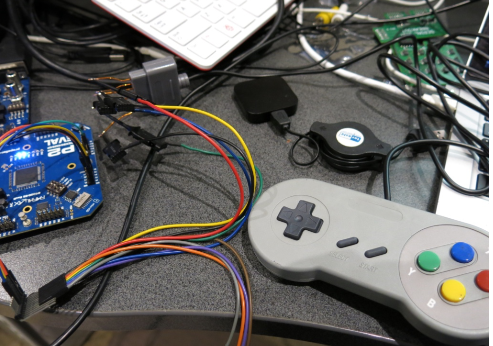
Be nice to have the actual mating connector for the game controller. Only wire I had that fits inside it was some thick enameled stuff I had lying about and took ages to scrape it off. Am loathed to cut the connector off but I might.
Good work, Roger. I have done more testing and I understand full FIFO loading now. Partial FIFO filling to be investigated.
RDFAST with wait takes 10-17 cycles, one more than RDLONG with the extra cycle at the start. RDBYTE, RDWORD & RDLONG have a fixed pre-read time of 3 cycles, then a variable read time of 1-8 cycles depending on egg beater hub RAM slice, then a fixed post-read time of 5 cycles, making a total of 9-16 assuming no long crossing that would add an extra cycle. WRBYTE, WRWORD, WRLONG & WMLONG have a fixed pre-write time of 3 cycles and a variable write time of 0-7 cycles, again assuming no long crossing.
The FIFO depth of 19 means 18 longs must be read in 18 cycles immediately after the first long. A random hub read or write will be delayed after RDFAST if the random read or write slice coincides with any of these 18 FIFO read slices. The post-read time of 5 cycles for RDFAST and pre-read or pre-write time of 3 cycles for the hub access add up to 8 cycles, which leaves a minimum time of 10 cycles between end of RDFAST with wait and start of random read/write to avoid the latter being delayed.
N.B. The 10 cycle minimum is increased by one cycle every time RFxxxx consumes a long when the FIFO is still filling. A long is consumed by every RFLONG, or by RFWORD that starts at bytes 2 or 3, or by RFBYTE at byte 3.
Well that's useful information @TonyB_. Here's the timing I think we have between the relevant instructions in my code.
Also audio is working now. It's hardly the best sounding stuff, being 4bit audio, but it is what it is and can be output over the A/V breakout board now.
I still have to check through the SPI pin IO and try to get the serial input working. But the basics with the game controller interface, that is video+audio+leds+game port is apparently all working so far. It does need to build with DEBUG mode in FlexSpin (the -gbrk option) for some reason and I'm still figuring out why it fails to start up properly without that. Might be PLL related as this was pure PASM without SPIN2, or it could need a delay after COG startup to sync the two correctly. So if you build this just use the -gbrk option.
The Gigatron ROM is found on github here..
https://github.com/kervinck/gigatron-rom
Latest code is attached - and it's moved to beta status now since it's essentially usable for all the basic Gigatron functions (with a game controller anyway).
For a non-blocking RDFAST, the max post-RDFAST ticks needed will be 17 (start filling) + 18 (fill complete) - 2 (non-blocking execution) = 33 ticks.
Yeah I am hoping we are mostly okay except that branch case. Looking at the branch code I think I can possibly rearrange it a bit to buy a few more clocks before we need to do the RDBYTE. The main thing is to not read from the FIFO before it is ready, that will lock up the system. If the other RDBYTE or WRBYTE cycles happen to be delayed a bit, it might corrupt video temporarily with an extra pixel on a line, but it may not be too noticeable unless it happens a lot. I just want to make sure it doesn't hang or something.
Why would the FIFO fill waste 17 clocks before it even starts reading???
Do you do ASMCLK at startup?
In the worst case, it needs to finish writing up to 8 or so longs and then wait a whole rotation before it reaches the slice it wants to start reading at.
Ha, no, FIFO writes would extend that further.
Excluding prior writes, but including the 2 ticks for execution, 17 is worst case for just RDFAST by itself. 10 is best case.
The 10..17 is made of 2 for execution, 2 for internal setup, 1..8 for hub slot align and read, and 5 for route/switching stages.
A plain RDLONG is 9..16 so is made of 2 for execution, 1 for internal setup, 1..8 for hub slot align and read, and 5 for route/switching stages.
BTW, FIFO writes are unlikely to be buffer delayed in the FIFO. Testing has proven they are always written to hubRAM ASAP, to the detriment of throughput.
Thinking about it a little more, that 33 ticks may not be right either. The 5 post-hubRAM stages won't matter since they are just like a pipeline so don't need to be emptied first. Then, 28 ticks after a non-blocking RDFAST should be clear.