Yeah, a smartpin timing mismatch recovering during vblank sounds fine to me. It would primarily be a debugging tool anyway.
Thanks. Yeah I was thinking about how it could be done this morning. It needs to measure the time (in pixel clocks) from the falling edge of DE on the last active scan line to the HSYNC edge on the next line at the start of vertical blanking. If this count is different to the expected configured front porch pixels then there is a mismatch and the code needs to resync the streamer output to the DE PWM timing, which might hopefully be a matter of a one off adjustment in the streamer by introducing some extra dummy pixel clocks. While the overload lasts this process would be continuous and likely mess up the analog output, but the digital output would at least start out correct at the start of the next frame and it would recover when the overload ceased. I might have some spare instruction cycles if I create a custom VSYNC sequence just for parallel RGB output. It's not critical but it's good to know whether something like this might be doable at some point. I'd need to find a smartpin mode that can time first pin edge to 2nd pin edge cases, surely one of the many modes does that...
Here's what I'm thinking about for this new parallel RGB feature to go into my P2 video driver.
To enable this output type you would nominate the digital output in the existing initialization register's "D" bit. Driver would then use the "V" bit to distinguish HDMI/DVI vs Parallel RGB. My setup APIs would need to be extended a little for this.
The (currently unused) mode dependent initialization register (RESERVED_1) would point to an additional block of configuration data used for parallel RGB. This block would include configuration data for:
a CLK pin & polarity bit
an optional DE pin & polarity bit
the base pin group for the start of 24 bit RGB data (0-7), ie. where Blue bit 0 pin begins.
24 bit data pin mask applied to this 24 bit RGB data sent over port A / B, to optionally reduce the number of active RGB pins from 24 down to something smaller, eg. for 12, 15, 18 bit LCD panels etc
an optional LCD backlight PWM pin & polarity bit and the backlight PWM frequency (~20Hz ... ~15kHz). The PWM duty cycle that controls backlight brightness can be changed dynamically via an API with something like setBacklight(@display, duty_value)
flags indicating whether:
the DE pin signal gets output or not
the additional VSYNC and HSYNC signals are output (the sync pins would be obtained from the existing initialization register data used in VGA mode)
the additional analog RGB signals are also output by DACs (DAC base taken from existing initialization register data used in VGA mode)
an optional control pin and polarity bit to enable LCD power, and a programmable delay applied after LCD power up before active video is sent out
I think this set of features should be useful for various cases of parallel LCDs or RGB encoders such as the TFP410. I've already proven my driver can do analog & digital RGB outputs at the same time.
All the LCD control pins bar HSYNC would be arbitrary. Probably the only constraint would be that the HSYNC pin would need to remain on a 4 bit boundary (as it is generated by DAC0), which is already the case today for the VGA output.
That DAC channel is used for HSYNC I think. Also I would want to keep the ability to output both VGA and parallel RGB simultaneously, so I don't have a spare in that case either. The streamer is fully used in that case. Given these constraints, the PWM smart pin output for DE is probably the best/only other option.
That idea might be possible. If I remember rightly, CMOD can leave DAC0 raw. Whatever you're doing for 24-bit parallel presumably can also apply to 32-bit parallel.
@evanh said:
That idea might be possible. If I remember rightly, CMOD can leave DAC0 raw. Whatever you're doing for 24-bit parallel presumably can also apply to 32-bit parallel.
Maybe, but I still really want to keep DAC0 avialable for an HSYNC signal when that is needed. Some LCD panels can actually use VSYNC/HSYNC instead of DE. It is already being generated for the analog case too, so all that related VGA code can simply remain the same.
The 32 bit parallel output thing brings up an interesting point though. Right now on my own board I am using 24 GPIO pins from P0-P23 for the RGB data, and the 4th channel (the "0" in R:G:B:0) wraps back around to P56-P63 on port B, but gets masked off with corresponding DIRB bits low in the driver so it has no effect. It might end up being the case that these extra 8 parallel bits can't overlap the DAC pins (not sure yet which gets priority). Hopefully the other PWM smart pins would take priority over the streamer, or else there is another constraint that they not be put in this region of pins. In any case, P0-P23 is quite a good choice of pins for RGB data, as most of the upper port B bits are already used for serial/flash anyway.
The parallel out doesn't go through the CSC, does it? because the CSC only cares about the bottom two bits... Though then you'd have to put the DE on a channel 0 pin.
@Wuerfel_21 said:
The parallel out doesn't go through the CSC, does it? because the CSC only cares about the bottom two bits... Though then you'd have to put the DE on a channel 0 pin.
Yes and then the video driver design wouldn't be able to work with my own LCD given my Voyager board's DE signal is P25 and my VGA output is on P35-P39. I can see it could be helpful to help resolve any DE to HSYNC phase offset change during overload though. Maybe I'll eventually look into adding some compensation code in the vertical blanking in case that happens. But that's low priority right now as overload is not a normal situation.
IIRC, in case of TFP410, only 16 lanes would suffice, in order to be able to transfer 24-bit RGB data + HSync + VSync +DE + PClk.
And even DE can be internally generated by TFP410, though under some restrictions related to each line's total pixel count versus HSync.
The 24-bit RGB data can be split 12 + 12, DDR style, but much easier than with HyperBus devices, because it has a programmable phase-delay, correlating data sampling position with respect to the pixel clock active edge(s).
P2 Sysclk would need to reach 2 x pixel clock (~2 x 165 MHz), to be able to keep with its maximum data rates (and also a very carefull layout), though.
@Yanomani said:
IIRC, in case of TFP410, only 16 lanes would suffice, in order to be able to transfer 24-bit RGB data + HSync + VSync +DE + PClk.
Yes it might be possible with a different video driver that streamed DDR output from a 32 bit frame buffer designed with that custom pixel format. But the P2 doesn't do DDR RGB in its LUT output modes, it only uses R:G:B:0 so it's just 24 bits of RGB data from my driver at all times, or a subset of their MSb's (or LSb's if you always use palette modes where you can control the colour range).
@rogloh said:
Hopefully the other PWM smart pins would take priority over the streamer, or else there is another constraint that they not be put in this region of pins. In any case, P0-P23 is quite a good choice of pins for RGB data, as most of the upper port B bits are already used for serial/flash anyway.
Smartpins are downstream so have inherent priority. Same for DAC channels - They have to be correctly selected to Cog/Streamer path or nothing will make it out.
@evanh said:
Smartpins are downstream so have inherent priority. Same for DAC channels
Umm, not sure about that for the DAC channels. I had a bug in my driver that was corrupting analog video out if the parallel streamer bits overlapped the DACs and the "e" bit was enabled in the "eppp" bits of the streamer commands. To me it seemed like it probably OR'd the parallel data or something and it could mess up the colours. Sync also might have been affected too. I fixed it by disabling the "e" bit when I had pure VGA out.
@rogloh said:
I had a bug in my driver that was corrupting analog video out if the parallel streamer bits overlapped the DACs and the "e" bit was enabled in the "eppp" bits of the streamer commands. To me it seemed like it probably OR'd the parallel data or something and it could mess up the colours. Sync also might have been affected too. I fixed it by disabling the "e" bit when I had pure VGA out.
That would be up-stream, inside the cog/streamer or maybe hub area. Prior to smartpins and pin config.
Pin config (WRPIN) selects which cog gets the quad channel DAC group. Given these are an 8-bit channel per pin, I can't see them being mixed with the OUT data after leaving the cog. It would have to be where the parallel data is aligned with the DAC data. That's only in the streamer itself I'd say.
It's funny (not) how with software you can quickly hack something new up and get it working in a few minutes and then discover that whenever you have to integrate everything fully with the existing code base and its provisioning APIs etc it takes hours/days of extra time to get it done. With my driver COG so full I've also had to resort to adding some overlays in LUT RAM at COG startup time to get this new parallel RGB mode setup code to run in the available space which complicates the matter too.
However I think I've got most of it figured out now. So far I only identified one new minor constraint for now, which is that the CLK and DE pins need to be on the same P2 port so they can be started at the same time with their DIRx bits going high on the same cycle. This is because we can't start both smart pins spanning port A and port B at the same time to align the phase (maybe we could if they are in the same pin span but that just limits them to being next to one another and doesn't help much). Maybe sometime later I can try to resync the DE startup to the right clock phase with waitx...I just don't want to think about that right now.
I've added 6 control bits in the top byte of the driver initialization register that can select which outputs are generated in parallel digital RGB mode:
bit 0 - disables CLK (CLK is generated by default, not sure why you wouldn't need a clock but whatever)
bit 1 - disables DE (DE is generated by default but can be disabled if not required and device only uses H+V syncs)
bit 2 - H&V SYNC outputs enabled
bit 3 - RGB DAC output pins enabled (set for simultaneous analog + digital RGB output)
bit 4 - optional backlight PWM pin enabled
bit 5 - optional power on pin enabled
The other two bits of this byte are already defined in this register and would get set as follows:
bit 6 - "V" bit set to 1 for parallel digital RGB output
bit 7 - "D" bit set to 1 for parallel digital RGB output
There are several other fields passed in now that control the extra pins:
HSYNC - P2 pin for DAC0 HSYNC output (also defines RGB pin outputs, these must start on a 4 pin group)
VSYNC - any P2 pin not already used (but this is not enforced)
CLK - LCD Clock pin
DE - LCD Display Enable pin (keep on same P2 port as the CLK pin)
B/L PWM - LCD backlight control pin
PWR - power on pin, can be used as a reset or "mute" function while video COG is not running or for power control to device (video begins after a settable delay once this pin is driven)
The last 4 pins above can each selectively be inverted if they are active low instead of active high by using an INVERT_PIN flag when passing in some pin numbers. H&V sync pin inversion is already defined in the video timing.
We also have a RGB mask, optional startup delay, and backlight frequency control. I think this lot should be sufficient for now.
To support the parallel RGB output mode in the SPIN2 code I've been extending my API to include a method of creating and passing a block of extended pin data (instead of the single VSYNC pin used in VGA mode), as well as two new output types DIGITAL_RGB24 and DIGITAL_RGB24_VGA, plus some new flags to select what you need.
To initialize the driver to run a LCD display using CLK+DE signals with a backlight operating at 200Hz with 10msec startup delay and simultaneously outputting VGA output on DAC pins you would use something like this:
I'm also thinking of allowing the set of "canned" resolution constants like RES_1024x768 etc to be passed in as the timing argument pointer. These would be made negative values and I could detect this special condition and look them up dynamically instead of using the timing argument as a pointer to a standard or custom timing struct. Saves a little extra code and it might be convenient for one line startups. But this is independent of the parallel RGB output mode stuff.
About 150 brand new lines of PASM2 were needed to fully integrate this parallel RGB code feature with my driver at initialization time and my LCD output is not working any more.
What fun this will now be to debug.
Maybe I should move over to proptool to gain those handy debug commands from PASM, unless debug from PASM also now works in flexspin?
So using those DEBUG statements in PASM2 made it a total breeze to debug the code. In about 10mins I found the offending one instruction in 150 - it turns out I was patching a CALLPA instruction's S field with a fixed address but it should be relative. Without this DEBUG printing output feature from PASM2 I know it would have taken me quite a while longer.
This was my CALLPA to do the vertical front porch blanking lines
patchvfp callpa #V_FP-0, #blank 'send vertical front porch lines
and I was patching it to get it to call some code to manage DE PWM output one line earlier:
sets patchvfp, #blank-1
but being relative it should just be this:
sub patchvfp, #1
or possibly better, something like this:
sets patchvfp, #(blank-patchvfp-1)
Still testing it but basically I now have LCD/digital RGB output support integrated into my P2 video driver and can use it do all the usual things such as multiple regions, text, palettes, external memory framebuffers etc...
Update: With some special palette setups I could potentially tweak this feature to even support CGA and EGA types of monitors too (having 4 and 6 digital outputs controlling the colour). I just don't have any old monitors for testing that.
Yep, I'm a fan of C for low level programming partly because it always has printf() as standard. It works really well for debugging when you've got all the source code and complete data on the hardware.
The plotting features of debug() takes that up a level and, what's more, debug() doesn't have to be Spin2 specific. Nothing stopping it working with BASIC, C and even Forth I'd imagine.
Being still unsatisfied with the composite video quality, I went ahead and recomputed all the relevant constants (well, some are still eyeballed). Seems significantly improved, though I only tested it on my capture card and by looking at colorbars through the oscilloscope.
Good work. I've been hoping for getting some better values for the composite quality which I know had NTSC looking oversaturated and PAL somewhat anemic in comparsion. I know we looked at some of this a while back when someone generous had access to that vectorscope and were trying to get those colour burst phases and levels to match up properly, but we then hit that 1Vpp DAC swing roadblock with PAL and NTSC and the P2 and it's not easily solved. To meet the proper composite video colour levels IIRC it would need to be able to drive to 1V and around negative 0.3V for the sync tips when terminated IIRC which exceeds the 1Vpp range of the 75ohm DAC in the P2, although the s-video output with its chroma split out on a separate channel was okay and wouldn't exceed the dynamic range. I'd not looked at any more of that stuff since then. Also I think Chip had some demo code using accurate calculations for computing the CFRQ parameter I wanted to try to incorporate in at some point.
I think I did have the composite sync stuff totally nailed, it's really just the colour modulator timing parameter or levels might still be off somewhere, IDK.
Yeah, it's all in the CSC parameters. The signal does end up kindof weak after leaving enough headroom above white level (some 0.55v black-to-white), maybe one of the other DAC modes is more appropriate. Then again, it's not that important if the display has AGC. Relatedly, Chip's settings get around the level issue to some extent by lowering the blanking level. That is very bad, because it will totally blow out the image on some displays (such as the s-video input on my capture card)
@Wuerfel_21 said:
Yeah, it's all in the CSC parameters. The signal does end up kindof weak after leaving enough headroom above white level (some 0.55v black-to-white), maybe one of the other DAC modes is more appropriate. Then again, it's not that important if the display has AGC. Relatedly, Chip's settings get around the level issue to some extent by lowering the blanking level. That is very bad, because it will totally blow out the image on some displays (such as the s-video input on my capture card)
That's right, and I agree reducing the sync tips/blanking level is a bit of a hack here. It would have been nice to be able to send 100% colour bars AND meet the standard voltage levels to achieve correct colour. It does not appear possible on the P2 to achieve PAL voltage levels and meet colour reference levels at the same time. You have to play with colour burst amplitude levels to try to compensate for the reduced DAC range and can't really match the standard voltages into 75 ohm loads. ie. you couldn't match a reference PAL colour bar composite video signal using the P2, and it's probably same with NTSC, you can only approximate it with some scaling but that throws all the specified chroma voltages off a bit and becomes hard to tune right on a scope as I found out.
I've added 6 control bits in the top byte of the driver initialization register that can select which outputs are generated in parallel digital RGB mode:
bit 0 - disables CLK (CLK is generated by default, not sure why you wouldn't need a clock but whatever)
So I finally found a use case for disabling the clock in my parallel output mode. This will be a good way to support old school CGA/MDA/EGA monitors that don't need a clock (or DE for that matter). My new RGB parallel output mode is maskable and will readily support 1, 2, 4, 6 colour bits per pixel anyway, so assuming the video timing is setup correctly my driver should be able to output to these old TTL monitors nicely. It would be a nostalgic laugh to see the P2 generate some graphics on older digital monitors like these if I can source one. It should still look nice and vibrant even with their limited colour palette range.
Since I've just added parallel digital output I have also been thinking about LVDS again and also located this thread https://forums.parallax.com/discussion/171516/p2-fpd-link-lvds-displays. I figure if I can get the processing done in less than 14 clocks per pixel it might (only) just be achievable to output LVDS using my driver. There would need to be a lot of limitations imposed though, like single region only, no mouse, no text render, no border, low refresh rate panels only ~24Hz?, either 4bpp or 8bpp gfx mode only, maybe with some pixel doubling (not sure). If I can't get pixel doubling it would not be possible to have a framebuffer for 1024x600x8bpp displays fit in internal hub RAM though it could be done for 4bpp. External RAM would have the capacity but again I'd need to see if there is any time for that in the code, and it would need some more rework to read external data one scan line earlier so the pixels are ready to be processed in time.
The thread above mentioned that 20MHz pixel clocks (low refresh) were possible on a particular LVDS display. I came up with an instruction sequence below that can generate 8 LVDS encoded pixels at a rate of 12 P2 clocks/pixel in its inner loop which is still under the budget of 14 P2 clocks for a 280MHz P2 clocking out 20MHz LVDS encoded pixels. However I would also need to read the input pixels from HUB to LUT and then write back to HUB once encoded and this adds 1.125 more clocks per pixel. It's already really tight and yet to be determined if its execution timing fits in with the loop overheads and HUB burst read/write delays etc. Perhaps 21 P2 clocks per pixel would be needed instead, but that only reduces the frame rate even more...
```
rdlut colours, ptra++ ' read in 4 coloured 8 bit pixels from LUTRAM input buffer
getbyte index, colours, #0 ' get first pixel colour (8bit colour index)
rdlut pixels, index ' read palette colour to translate to 7x4 bit LVDS patterns (18 or 24 bit colour)
getbyte index, colours, #1 ' get second pixel colour
rdlut pixels+1, index ' get second pixel pattern
setnib pixels, pixels+1, #7 ' merge new portion with 28 bits of first long
shr pixels+1, #4 ' align second long
wrlut pixels, ptrb++ ' write first long to output buffer in LUTRAM
getbyte index, colours, #2 ' get third pixel colour
rdlut pixels+2, index ' get third pixel pattern
setbyte pixels+1, pixels+2, #3 ' merge new portion with 24 bits of second long
shr pixels+2, #8 ' align third long
wrlut pixels+1, ptrb++ ' write second long to output buffer
getbyte index, colours, #3 ' get fourth pixel colour
rdlut pixels+3, index ' get fourth pixel pattern
setnib pixels+2, pixels+3, #5 ' merge new portion with 20 bits of third long
shr pixels+3, #4 ' align fourth long
setbyte pixels+2, pixels+3, #3 ' merge new portion with 24 bits of third long
shr pixels+3, #8 ' align fourth long
wrlut pixels+2, ptrb++ ' write third long to output buffer
rdlut colours, ptra++ ' continue with next four pixels...writing four further longs to LUT (7 total)
getbyte index, colours, #0
rdlut pixels+4, index
setword pixels+3, pixels+4, #1
shr pixels+4, #16
wrlut pixels+3, ptrb++
getbyte index, colours, #1
rdlut pixels+5, index
setnib pixels+4, pixels+5, #3
shr pixels+5, #4
setword pixels+4, pixels+5, #1
shr pixels+5, #16
wrlut pixels+4, ptrb++
getbyte index, colours, #2
rdlut temp, index
setbyte pixels+5, temp, #1
shr temp, #8
setword pixels+5, temp, #1
wrlut pixels+5, ptrb++
getbyte index, colours, #3
rdlut pixels+6, index
rolnib pixels+6, a, #4
wrlut pixels+6, ptrb++
' Total loop for 8 pixels = 10xRDLUT(3) + 7xWRLUT(2) + 26x2 other instructions = 30+14+52 = 96 clocks or 12 clocks/pixel
' plus
' 4 pixels read per long on input in 8bpp mode (~ 0.25 clocks/pixel in SETQ2 read burst)
' 7 longs generated for 8 pixels on output (0.875 clocks/pixels to write to hub)
' making 12 + 0.25 + 0.875 = 13.125 clocks/pixel exluding other loop overheads etc.
' This number must remain below 14 after the overheads. It will be very tight!
bit 0 - disables CLK (CLK is generated by default, not sure why you wouldn't need a clock but whatever)
So I finally found a use case for disabling the clock in my parallel output mode. This will be a good way to support old school CGA/MDA/EGA monitors that don't need a clock (or DE for that matter). My new RGB parallel output mode is maskable and will readily support 1, 2, 4, 6 colour bits per pixel anyway, so assuming the video timing is setup correctly my driver should be able to output to these old TTL monitors nicely. It would be a nostalgic laugh to see the P2 generate some graphics on older digital monitors like these if I can source one. It should still look nice and vibrant even with their limited colour palette range.
Leave LVDS for Chip to add, alongside TMDS, as a new mode for CMOD.
Funnily, I had originally assumed DVI/HDMI used the same encoding as LVDS. I first bumped into LVDS in a system called Camera-Link in the late 1990's. Used for defect detection of products on a production line. The software was horribly buggy. Kept corrupting its config files. And the system was replaced with something only marginally better.


Comments
Thanks. Yeah I was thinking about how it could be done this morning. It needs to measure the time (in pixel clocks) from the falling edge of DE on the last active scan line to the HSYNC edge on the next line at the start of vertical blanking. If this count is different to the expected configured front porch pixels then there is a mismatch and the code needs to resync the streamer output to the DE PWM timing, which might hopefully be a matter of a one off adjustment in the streamer by introducing some extra dummy pixel clocks. While the overload lasts this process would be continuous and likely mess up the analog output, but the digital output would at least start out correct at the start of the next frame and it would recover when the overload ceased. I might have some spare instruction cycles if I create a custom VSYNC sequence just for parallel RGB output. It's not critical but it's good to know whether something like this might be doable at some point. I'd need to find a smartpin mode that can time first pin edge to 2nd pin edge cases, surely one of the many modes does that...
Yep, there's many modes that have A->B measuring. Never tested the feature myself, always just A->A instead, ...
Here's what I'm thinking about for this new parallel RGB feature to go into my P2 video driver.
To enable this output type you would nominate the digital output in the existing initialization register's "D" bit. Driver would then use the "V" bit to distinguish HDMI/DVI vs Parallel RGB. My setup APIs would need to be extended a little for this.
The (currently unused) mode dependent initialization register (RESERVED_1) would point to an additional block of configuration data used for parallel RGB. This block would include configuration data for:
flags indicating whether:
an optional control pin and polarity bit to enable LCD power, and a programmable delay applied after LCD power up before active video is sent out
I think this set of features should be useful for various cases of parallel LCDs or RGB encoders such as the TFP410. I've already proven my driver can do analog & digital RGB outputs at the same time.
All the LCD control pins bar HSYNC would be arbitrary. Probably the only constraint would be that the HSYNC pin would need to remain on a 4 bit boundary (as it is generated by DAC0), which is already the case today for the VGA output.
Hmm, couldn't you just generate DE with the streamer? (would have to be in that DAC0 channel that gets zeroes during active display).
That DAC channel is used for HSYNC I think. Also I would want to keep the ability to output both VGA and parallel RGB simultaneously, so I don't have a spare in that case either. The streamer is fully used in that case. Given these constraints, the PWM smart pin output for DE is probably the best/only other option.
That idea might be possible. If I remember rightly, CMOD can leave DAC0 raw. Whatever you're doing for 24-bit parallel presumably can also apply to 32-bit parallel.
Maybe, but I still really want to keep DAC0 avialable for an HSYNC signal when that is needed. Some LCD panels can actually use VSYNC/HSYNC instead of DE. It is already being generated for the analog case too, so all that related VGA code can simply remain the same.
The 32 bit parallel output thing brings up an interesting point though. Right now on my own board I am using 24 GPIO pins from P0-P23 for the RGB data, and the 4th channel (the "0" in R:G:B:0) wraps back around to P56-P63 on port B, but gets masked off with corresponding DIRB bits low in the driver so it has no effect. It might end up being the case that these extra 8 parallel bits can't overlap the DAC pins (not sure yet which gets priority). Hopefully the other PWM smart pins would take priority over the streamer, or else there is another constraint that they not be put in this region of pins. In any case, P0-P23 is quite a good choice of pins for RGB data, as most of the upper port B bits are already used for serial/flash anyway.
The parallel out doesn't go through the CSC, does it? because the CSC only cares about the bottom two bits... Though then you'd have to put the DE on a channel 0 pin.
Yes and then the video driver design wouldn't be able to work with my own LCD given my Voyager board's DE signal is P25 and my VGA output is on P35-P39. I can see it could be helpful to help resolve any DE to HSYNC phase offset change during overload though. Maybe I'll eventually look into adding some compensation code in the vertical blanking in case that happens. But that's low priority right now as overload is not a normal situation.
IIRC, in case of TFP410, only 16 lanes would suffice, in order to be able to transfer 24-bit RGB data + HSync + VSync +DE + PClk.
And even DE can be internally generated by TFP410, though under some restrictions related to each line's total pixel count versus HSync.
The 24-bit RGB data can be split 12 + 12, DDR style, but much easier than with HyperBus devices, because it has a programmable phase-delay, correlating data sampling position with respect to the pixel clock active edge(s).
P2 Sysclk would need to reach 2 x pixel clock (~2 x 165 MHz), to be able to keep with its maximum data rates (and also a very carefull layout), though.
Yes it might be possible with a different video driver that streamed DDR output from a 32 bit frame buffer designed with that custom pixel format. But the P2 doesn't do DDR RGB in its LUT output modes, it only uses R:G:B:0 so it's just 24 bits of RGB data from my driver at all times, or a subset of their MSb's (or LSb's if you always use palette modes where you can control the colour range).
Smartpins are downstream so have inherent priority. Same for DAC channels - They have to be correctly selected to Cog/Streamer path or nothing will make it out.
Umm, not sure about that for the DAC channels. I had a bug in my driver that was corrupting analog video out if the parallel streamer bits overlapped the DACs and the "e" bit was enabled in the "eppp" bits of the streamer commands. To me it seemed like it probably OR'd the parallel data or something and it could mess up the colours. Sync also might have been affected too. I fixed it by disabling the "e" bit when I had pure VGA out.
Raising OUT on a DAC pin enables the ADC (and thus presumably disables DAC?)
That would be up-stream, inside the cog/streamer or maybe hub area. Prior to smartpins and pin config.
Pin config (WRPIN) selects which cog gets the quad channel DAC group. Given these are an 8-bit channel per pin, I can't see them being mixed with the OUT data after leaving the cog. It would have to be where the parallel data is aligned with the DAC data. That's only in the streamer itself I'd say.
Does both at once. DAC drives pin and ADC reads pin. ADC then feeds IN with sigma-delta(PDM) bitstream.
It would be nice to know what caused the real problem in this overlap. Luckily it was a simple fix in the end.
It's funny (not) how with software you can quickly hack something new up and get it working in a few minutes and then discover that whenever you have to integrate everything fully with the existing code base and its provisioning APIs etc it takes hours/days of extra time to get it done. With my driver COG so full I've also had to resort to adding some overlays in LUT RAM at COG startup time to get this new parallel RGB mode setup code to run in the available space which complicates the matter too.
However I think I've got most of it figured out now. So far I only identified one new minor constraint for now, which is that the CLK and DE pins need to be on the same P2 port so they can be started at the same time with their DIRx bits going high on the same cycle. This is because we can't start both smart pins spanning port A and port B at the same time to align the phase (maybe we could if they are in the same pin span but that just limits them to being next to one another and doesn't help much). Maybe sometime later I can try to resync the DE startup to the right clock phase with waitx...I just don't want to think about that right now.
I've added 6 control bits in the top byte of the driver initialization register that can select which outputs are generated in parallel digital RGB mode:
bit 0 - disables CLK (CLK is generated by default, not sure why you wouldn't need a clock but whatever)
bit 1 - disables DE (DE is generated by default but can be disabled if not required and device only uses H+V syncs)
bit 2 - H&V SYNC outputs enabled
bit 3 - RGB DAC output pins enabled (set for simultaneous analog + digital RGB output)
bit 4 - optional backlight PWM pin enabled
bit 5 - optional power on pin enabled
The other two bits of this byte are already defined in this register and would get set as follows:
bit 6 - "V" bit set to 1 for parallel digital RGB output
bit 7 - "D" bit set to 1 for parallel digital RGB output
There are several other fields passed in now that control the extra pins:
HSYNC - P2 pin for DAC0 HSYNC output (also defines RGB pin outputs, these must start on a 4 pin group)
VSYNC - any P2 pin not already used (but this is not enforced)
CLK - LCD Clock pin
DE - LCD Display Enable pin (keep on same P2 port as the CLK pin)
B/L PWM - LCD backlight control pin
PWR - power on pin, can be used as a reset or "mute" function while video COG is not running or for power control to device (video begins after a settable delay once this pin is driven)
The last 4 pins above can each selectively be inverted if they are active low instead of active high by using an INVERT_PIN flag when passing in some pin numbers. H&V sync pin inversion is already defined in the video timing.
We also have a RGB mask, optional startup delay, and backlight frequency control. I think this lot should be sufficient for now.
To support the parallel RGB output mode in the SPIN2 code I've been extending my API to include a method of creating and passing a block of extended pin data (instead of the single VSYNC pin used in VGA mode), as well as two new output types DIGITAL_RGB24 and DIGITAL_RGB24_VGA, plus some new flags to select what you need.
PUB digitalPinInfo(pinInfoAddr, hsyncPin, vsyncPin, clkPin, dePin, backLightPin, powerPin, backLightFreq, startupDelayUs, rgbMask24)
    longmove(pinInfoAddr, @hsyncPin, 9)
    return pinInfoAddr
To initialize the driver to run a LCD display using CLK+DE signals with a backlight operating at 200Hz with 10msec startup delay and simultaneously outputting VGA output on DAC pins you would use something like this:
Compared to this, VGA is a little simpler with the arguments, and is still done the same way...
I'm also thinking of allowing the set of "canned" resolution constants like RES_1024x768 etc to be passed in as the timing argument pointer. These would be made negative values and I could detect this special condition and look them up dynamically instead of using the timing argument as a pointer to a standard or custom timing struct. Saves a little extra code and it might be convenient for one line startups. But this is independent of the parallel RGB output mode stuff.
About 150 brand new lines of PASM2 were needed to fully integrate this parallel RGB code feature with my driver at initialization time and my LCD output is not working any more.
What fun this will now be to debug.
Maybe I should move over to proptool to gain those handy debug commands from PASM, unless debug from PASM also now works in flexspin?
Yes, it does now ;p Compile with
-gbrkCool. I will have to figure it out and give it a try.
Update: Great!
So using those DEBUG statements in PASM2 made it a total breeze to debug the code. In about 10mins I found the offending one instruction in 150 - it turns out I was patching a CALLPA instruction's S field with a fixed address but it should be relative. Without this DEBUG printing output feature from PASM2 I know it would have taken me quite a while longer.
This was my CALLPA to do the vertical front porch blanking lines
and I was patching it to get it to call some code to manage DE PWM output one line earlier:
but being relative it should just be this:
or possibly better, something like this:
Still testing it but basically I now have LCD/digital RGB output support integrated into my P2 video driver and can use it do all the usual things such as multiple regions, text, palettes, external memory framebuffers etc...
Update: With some special palette setups I could potentially tweak this feature to even support CGA and EGA types of monitors too (having 4 and 6 digital outputs controlling the colour). I just don't have any old monitors for testing that.
Yep, I'm a fan of C for low level programming partly because it always has printf() as standard. It works really well for debugging when you've got all the source code and complete data on the hardware.
The plotting features of debug() takes that up a level and, what's more, debug() doesn't have to be Spin2 specific. Nothing stopping it working with BASIC, C and even Forth I'd imagine.
Being still unsatisfied with the composite video quality, I went ahead and recomputed all the relevant constants (well, some are still eyeballed). Seems significantly improved, though I only tested it on my capture card and by looking at colorbars through the oscilloscope.
    ONE_IRE = 255.0 / 180.0
    BLANKING_LEVEL = ONE_IRE*40.0
    PEDESTAL = ONE_IRE*7.5 ' NTSC only, other standards (including NTSC-J) don't have pedestal

    BLANK_LEVEL = round(BLANKING_LEVEL)

    B2W_NTSC = ONE_IRE*100.0 - PEDESTAL
    YSCALE_NTSC = 127.0*(B2W_NTSC/255.0)
    IQSCALE_NTSC = YSCALE_NTSC * 1.47

    B2W_PAL = ONE_IRE*100.0
    YSCALE_PAL = 127.0*(B2W_PAL/255.0)
    UVSCALE_PAL = YSCALE_PAL * 1.33 ' Can't set correct amplitude (around 1.47) because weird overflow?


    CY_CVBS_SDTV = (round(0.299*YSCALE_NTSC)&$FF)<<24 + (round(0.587*YSCALE_NTSC)&$FF)<<16 + (round(0.114*YSCALE_NTSC)&$FF)<<8 + round(BLANKING_LEVEL+PEDESTAL)
    CI_CVBS_SDTV = (round(+0.5959*IQSCALE_NTSC)&$FF)<<24 + (round(-0.2746*IQSCALE_NTSC)&$FF)<<16 + (round(-0.3216*IQSCALE_NTSC)&$FF)<<8 + round(BLANKING_LEVEL)
    CQ_CVBS_SDTV = (round(+0.2115*IQSCALE_NTSC)&$FF)<<24 + (round(-0.5227*IQSCALE_NTSC)&$FF)<<16 + (round(+0.3112*IQSCALE_NTSC)&$FF)<<8 + 128

    CY_PAL      = (round(0.299*YSCALE_PAL)&$FF)<<24 + (round(0.587*YSCALE_PAL)&$FF)<<16 + (round(0.114*YSCALE_PAL)&$FF)<<8 + round(BLANKING_LEVEL)
    CU_PAL      = (round(-0.147*UVSCALE_PAL)&$FF)<<24 + (round(-0.289*UVSCALE_PAL)&$FF)<<16 + (round(+0.436*UVSCALE_PAL)&$FF)<<8 + round(BLANKING_LEVEL)
    CV_PAL_ODD  = (round(+0.615*UVSCALE_PAL)&$FF)<<24 + (round(-0.515*UVSCALE_PAL)&$FF)<<16 + (round(-0.100*UVSCALE_PAL)&$FF)<<8 + 128
    CV_PAL_EVEN = (round(-0.615*UVSCALE_PAL)&$FF)<<24 + (round(+0.515*UVSCALE_PAL)&$FF)<<16 + (round(+0.100*UVSCALE_PAL)&$FF)<<8 + 128

    COLOUR_BURST_NTSC = $7C9900_01
    COLOUR_BURST_PAL  = $D8A351_01
Comparsion time
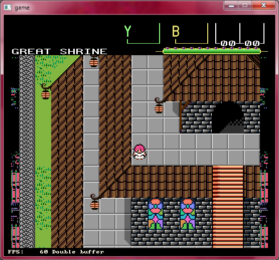
(raw screenshots from my capture card)
Roger's original constants
very cool
My earlier eyeballed constants
The new constants in this post
For comparsion, same scene in PC version
(well, the ROM on the P2 sd card is a bit outdated, thus the map name being "???". Also, different input config.)
Good work. I've been hoping for getting some better values for the composite quality which I know had NTSC looking oversaturated and PAL somewhat anemic in comparsion. I know we looked at some of this a while back when someone generous had access to that vectorscope and were trying to get those colour burst phases and levels to match up properly, but we then hit that 1Vpp DAC swing roadblock with PAL and NTSC and the P2 and it's not easily solved. To meet the proper composite video colour levels IIRC it would need to be able to drive to 1V and around negative 0.3V for the sync tips when terminated IIRC which exceeds the 1Vpp range of the 75ohm DAC in the P2, although the s-video output with its chroma split out on a separate channel was okay and wouldn't exceed the dynamic range. I'd not looked at any more of that stuff since then. Also I think Chip had some demo code using accurate calculations for computing the CFRQ parameter I wanted to try to incorporate in at some point.
I think I did have the composite sync stuff totally nailed, it's really just the colour modulator timing parameter or levels might still be off somewhere, IDK.
Yeah, it's all in the CSC parameters. The signal does end up kindof weak after leaving enough headroom above white level (some 0.55v black-to-white), maybe one of the other DAC modes is more appropriate. Then again, it's not that important if the display has AGC. Relatedly, Chip's settings get around the level issue to some extent by lowering the blanking level. That is very bad, because it will totally blow out the image on some displays (such as the s-video input on my capture card)
That's right, and I agree reducing the sync tips/blanking level is a bit of a hack here. It would have been nice to be able to send 100% colour bars AND meet the standard voltage levels to achieve correct colour. It does not appear possible on the P2 to achieve PAL voltage levels and meet colour reference levels at the same time. You have to play with colour burst amplitude levels to try to compensate for the reduced DAC range and can't really match the standard voltages into 75 ohm loads. ie. you couldn't match a reference PAL colour bar composite video signal using the P2, and it's probably same with NTSC, you can only approximate it with some scaling but that throws all the specified chroma voltages off a bit and becomes hard to tune right on a scope as I found out.
So I finally found a use case for disabling the clock in my parallel output mode. This will be a good way to support old school CGA/MDA/EGA monitors that don't need a clock (or DE for that matter). My new RGB parallel output mode is maskable and will readily support 1, 2, 4, 6 colour bits per pixel anyway, so assuming the video timing is setup correctly my driver should be able to output to these old TTL monitors nicely. It would be a nostalgic laugh to see the P2 generate some graphics on older digital monitors like these if I can source one. It should still look nice and vibrant even with their limited colour palette range.
Since I've just added parallel digital output I have also been thinking about LVDS again and also located this thread https://forums.parallax.com/discussion/171516/p2-fpd-link-lvds-displays. I figure if I can get the processing done in less than 14 clocks per pixel it might (only) just be achievable to output LVDS using my driver. There would need to be a lot of limitations imposed though, like single region only, no mouse, no text render, no border, low refresh rate panels only ~24Hz?, either 4bpp or 8bpp gfx mode only, maybe with some pixel doubling (not sure). If I can't get pixel doubling it would not be possible to have a framebuffer for 1024x600x8bpp displays fit in internal hub RAM though it could be done for 4bpp. External RAM would have the capacity but again I'd need to see if there is any time for that in the code, and it would need some more rework to read external data one scan line earlier so the pixels are ready to be processed in time.
The thread above mentioned that 20MHz pixel clocks (low refresh) were possible on a particular LVDS display. I came up with an instruction sequence below that can generate 8 LVDS encoded pixels at a rate of 12 P2 clocks/pixel in its inner loop which is still under the budget of 14 P2 clocks for a 280MHz P2 clocking out 20MHz LVDS encoded pixels. However I would also need to read the input pixels from HUB to LUT and then write back to HUB once encoded and this adds 1.125 more clocks per pixel. It's already really tight and yet to be determined if its execution timing fits in with the loop overheads and HUB burst read/write delays etc. Perhaps 21 P2 clocks per pixel would be needed instead, but that only reduces the frame rate even more...
```
```
Those things were ugly hacks even then!
Leave LVDS for Chip to add, alongside TMDS, as a new mode for CMOD.
Funnily, I had originally assumed DVI/HDMI used the same encoding as LVDS. I first bumped into LVDS in a system called Camera-Link in the late 1990's. Used for defect detection of products on a production line. The software was horribly buggy. Kept corrupting its config files. And the system was replaced with something only marginally better.