

Feedback on Out-Of-Box Experience when Just Getting Started
 whicker
Posts: 749
whicker
Posts: 749
I bought a new Windows 10 laptop. I decided to "play dumb and innocent" as I tried to get the P2 EVAL board working as if I purchased it today.
I started at the shop page https://www.parallax.com/product/propeller-2-evaluation-board-rev-c/
Things went awry when I plugged in the USB cable without having the parallax FTDI drivers installed. I was working with a set of "fresh eyes". Detached and intentionally forgetting what I already knew, I documented my path in detail into the weeds. But I'll spare all the screenshots and writeup. I'll just cut to the chase.
I am suggesting that on the Downloads & Resources tab, underneath resource links, that a link is given to the Parallax drivers:
https://www.parallax.com/package/parallax-ftdi-usb-drivers-for-windows/
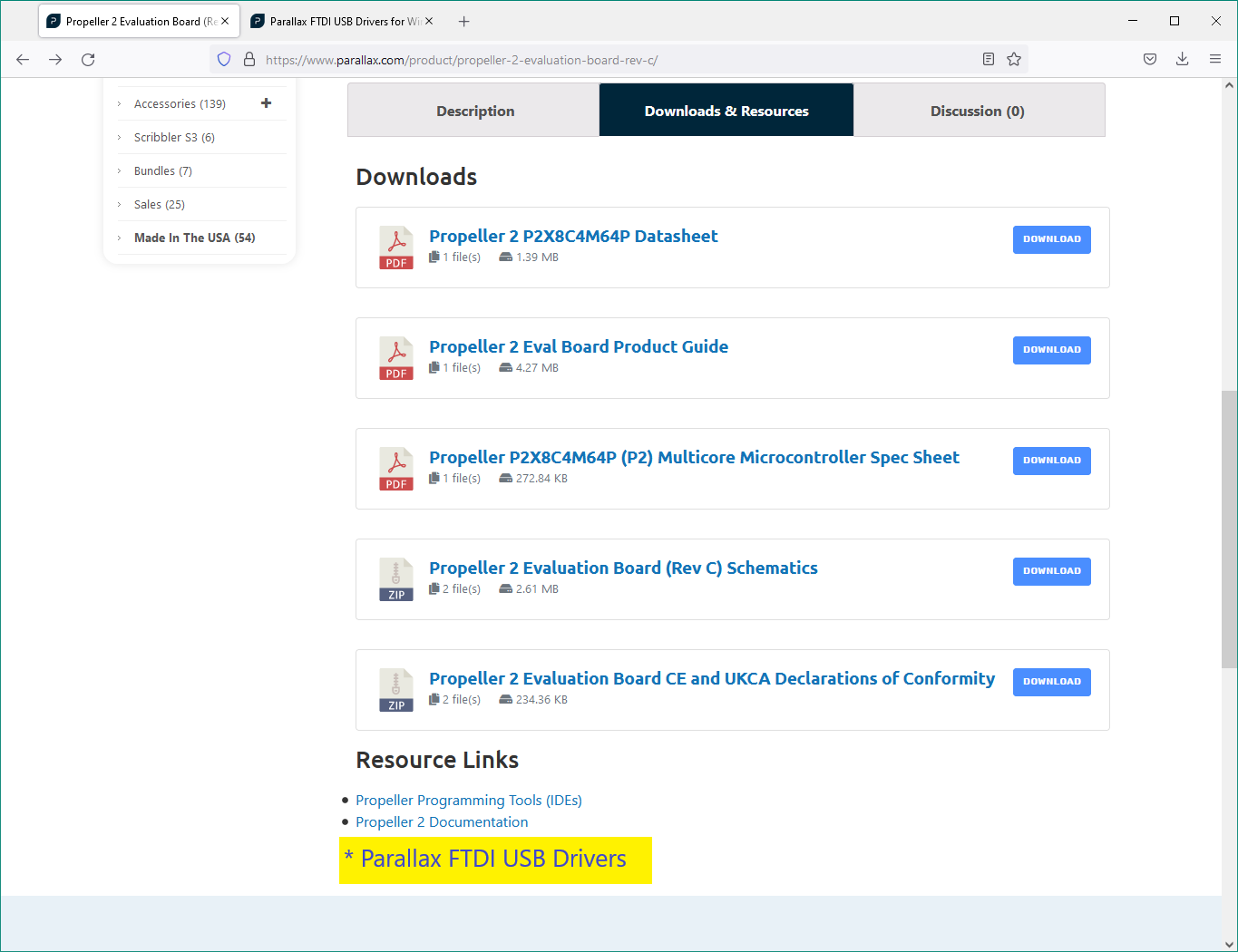
This is so that the new purchaser understands that they need to install custom Parallax drivers, and that plugging in the board will not "just work". Windows Update will lead you quite a ways down a bad path, but not ultimately find the correct drivers.
P2 Edge:
Similarly, I performed another thought experiment with the P2 Edge Breadboard and Mini Breakout Board.
Underneath the Resource Links for both of these products, there should be a link to Parallax Prop Plug (#32201). It is not okay to mention it in passing in the Specifications section, as it is easily missed and forgotten.
In the PDF documentation as well, there is no mention of drivers. It's just made to seem like 'plug it in'. Again, I know this seems obvious, but no it really isn't. Getting things connected and communicating is like 80% of the work.
Perhaps in-between the two paragraphs below, add...
If this is your first time using the Prop Plug, you will need to install the necessary Windows or Mac USB driver on your computer. Download links are available on the Prop Plug Download page. Please note, installing the Propeller Tool Software for Windows also installs the necessary USB drivers for the Prop Plug.
3. Prop Plug Programming Header The P2 Edge Module is programmed by the Parallax Prop Plug programming tool (#32201). To accommodate the Prop Plug, there is a dedicated 4-pin programming and debugging header. The pins are marked ▽ △ RES VSS, and correspond to the pin labelling on the Prop Plug adapter. Connect the Prop Plug to your computer with a suitable USB cable. Then, insert the Prop Plug onto the header pins with the Prop Plug components facing upward. The upward orientation allows you to see the RX and TX activity LEDs on the Prop Plug while programming or debugging data is being transmitted.
Comments
I'm confused here.
I think there are no 'Parallax custom drivers', just the FTDI ones. That means the best driver (ideally) should be the latest FTDI one.
That seems to be : Windows* 2021-07-15 2.12.36.4 2.12.36.4
In an ideal world, Windows should know about FTDI drivers and install the latest ones, when it sees a FTDI device plugged in.
If Windows update drops the ball, it would help to document that on Parallax.
FTDI have been dropping the ball for a while now. At this point I desperately avoid their chips. For most designs I use either the mcp2200 or xr21v1410. Both work with windows built-in drivers and don't require a download or a trip to Windows Update.
Indeed that FTDI 'got greedy' and opened the door for competitors.
I'm still wondering if Parallax is unnecessarily customizing something in a device descriptor or other string that causes Windows to avoid pairing the normal FTDI driver.
For example, instead of showing up as a COM port serial port, it initially gets listed under "unknown devices".
I think the Prop Tool also installs the FTDI virtual com port drivers.
But, I think Windows 10 comes with (or automatically installs) the FTDI virtual com port drivers.
It does not. I have tested this.
I just said in my first post that it does not.
Interesting... Not sure I've tried with a fresh Windows install in a while...
But, this Sparkfun guide says it "may" work without installing drivers:
https://learn.sparkfun.com/tutorials/how-to-install-ftdi-drivers/all
This is RS232R chip, but think drivers are the same...
I know nothing about FTDIs greed. I do know Windows does as it pleases. We use USB Ethernet with the bog standard descriptor and PID/VID, and it forgets about this all the time. And needs a “driver” to be installed which is nothing but a text file telling it “yes, you in fact do know this”. So I’d be a bit wary blaming FTDI here. It might well just windows being windows.
FTDI doesn't use a USB standard protocol; The driver is, in fact, a driver, and whether it's available via Windows Update varies from month to month, and that depends on FTDI. Furthermore, they've gone to great lengths to punish the victims of supply chain poisoning without doing anything to fix the problem.
This is an excellent e suggestion of focusing on the user experience, with
a particular specific example of what can be improved. It is part of
the broader exercise of User Centric design. Parallax may want to
consult with a user experience professional such as @UxMonty on
twitter A friend of mine, he regularly reminds me to focus on my work
from the point of view of the user, not the technology.
There are many more such examples. I try to minimize my posts, and
people are kind enough to respond, often by referencing obscure
documents. So an index into all of the scattered documents would be
most helpful.
The lexicon was a good step. Really it should be adopted by Parallax.
I know it is a huge amount of work just to create all of the
documentation, but high level introductions are also needed. Let us
give recent examples.
There is no guide to when to use which language. Slowly, very slowly,
I am creating such a guide in my head.
Thee is no guide to when to use the P2 versus a cheaper chip like the
ESP32. Okay, hard real time control is one example. I think High
Frequency I/O is another example. I think I read that at 300Mhz, you
can do I/O every 3.3 nano seconds. Did I get that right? Really phenomenal. But what about
20Mhz? At what frequency do you beat the competition? Tell the world about your strengths.
There is no high level guide to the software model. There was a
recent discussion about relative addressing. where I was reminded
that Register and LUTRAM addresses store 32 bits. Hubram addresses
store 8 bits. Wait a minute. Does that mean that in one round robin
cycle by FIFO, I can only load 8 x8 bits of hub ram? Ouch. I thought
in one round robin cycle, it would load 8 x 32 bits. It is really sad
that I do not yet have in my mind a high level model of how this chip
works. I am actually drafting such a document, but am quite confident
it still has too many mistakes to publish.
I will repeat there is no high level guide to PASM. The recent
discussion about "ROL D,{#}S {WC/WZ/WCZ} Syntax question" I still
mostly do not understand it.
There is a term called "software archeology". Where one reads the
source code to figure out how the system works. Quite a painful
process. I feel like i have been reading specific documentations, to
figure out how the whole system works. I have even been reading
source code, of Taqoz (Beautifully commented, thank you peter) and tried but failed to read the Spin2
interpreter source code, in order to figure out how this system works.
It is all very painful, very interesting, but painful, and slows down my progress.
Truth to be told, I have not bought a board yet. I still have not
figured out if this chip is a brilliant bottom up design, or if it is
too detail oriented, designed by an electrical engineer without enough
emphasis on getting the abstractions right. Several times I have
jumped away, looked at other chips, but still none look as promising
as this chip. Eventually I will know enough to make an intelligent
decision as to whether this chip meets my needs or not.
Which brings me back to my earlier point that it would be great to
have a high level market analysis. Where is this chip unique in what
it can do. When should one use a cheaper chip, like the ESP32?
And of course the rising competition is the Risc-v chip. All open
source, and dominated by India and China. Even used in the ESP32. One should not
underestimate them. A lot of people will say "Open Source", I want
that. Or "Cheap", I want that. They just do not know enough to
understand their limitations. Which is why Parallax needs a simple
clear argument why they are better then those two competitors.
Sorry if I am critical, I hope it helps you. Personally I think it is
brilliant, what you have done, how you hire americans, rather than out
sourcing to India, and that you are Chip owned, rather than venture
capital owned.
Keep up the great work.
Chris
One correction to the above:
While HubRAM is byte addressable, and therefore functionally 8 bits wide, the RAM blocks are 32 bits wide. The animation found in the Hub section of the Parallax Propeller 2 Documentation shows how the round-robin access works.
I'd also say that if the design process focusses on abstraction you never get facilities like the instruction skipping. Yes the chip would be easier to understand without the facility, but it wouldn't be as powerful.
@whicker,
yes it is sometimes painful, but parallax documentation states that you should install the drivers or PropTool BEFORE connecting the device. Then everythig usually workes out fine in any Windows Version.
@lozinski,
So Chris I really enjoy your posts and the effort you are putting into documentation for beginners, because I live way to long in the Parallax Universe to stumble over those miss named things like COGs=CORES etc.
The P1 documentation accessible over the PropTool is in my opinion the quality goal the P2 documentation need to reach.
In my not at all humble opinion one needs to not just read the P1 documentation, but PROGRAM the P1 for a couple of weeks to get a feeling for the quite different approach you need in software to get the jump/difference between threads and real parallel running cores.
Do simple stuff, USING the 'Propeller Way' to program parallel processes WITHOUT "interrupts, predefined Pin functions (SPI does just work if on Pins XX but then you can't use yyy)", instead loadable 'drivers' for whatever hardware you want to use on any pin.
This is a huge one for P1 and P2. Any function on any pin with just one Chip not 15+ Chip variants having 2xIC2 but then no second SPI except you use pins 2,5,7, whathever.
Same goes for board layout. Being able to place components whereever they fit best and just use the pins physically next to it is quite a winner.
And YES the P1 not the P2. Just to get (grook?) the different style of programming needed to understand the kind of different way to think about parallel programming.
Because on the P1 it is way more easy to understand the pincip. And THEN you should start with the P2 because a lot of features the P2 has got developed are building on the foundation of the P1.
The point I want to make here that 'this chip is a brilliant bottom up design'. But you need to think different to program it.
For most of the people here in the Forum it was/is still a jump from P1 to P2 but we mostly are adapted to Chips thinking and went a long way while the P2 was developed. While programming P1 ones.
Not so for newcomers. Both Propeller Chips are exotic (feral?) cats not normal house cats.
I like your term of "software archeology", because I program in COBOL, still, sometimes, because they throw money at me.
But this is currently the only way to go as a programmer, grab the pieces, build something, explore the way things are done. No programmer EVER was able to understand and program a computer thru reading all available documentation.
You have do do it. Get Hardware, run something, repeat.
Someone has to make @Potatohead long threads,
Enjoy!
Mike
Right. Basically it goes like this:
Jumping straight into the P2 waters and bypassing the P1 might work for some but going the P1 route first is what I did (and I only started last August) and it worked.
@msrobots said
I will read the P1 docs. I have no problem with the general approach the P2 takes. I have no problem thinking about distributed systems. I was specifically looking for a manycore chip that did something like this. My problem is grasping a high level understanding of the chip, so that I can decide if it will support my project or not.
@AJL, It is still not quite clear to me. So I went back to the documentation.
In the rest of this document, the most recent changes are in bold.
Here is what I think me introductory documentation should say:
Hub RAM is divided into n slices. One slice for each Cog/Core. Meaning 8 slices on the P2. The cogs all access HubRAM simultaneously in a round robin fashion, each accessing a different slice .
HubRam slices are accessed using 20 bit addresses. The lowest 2 bits specify the byte within a word. The next lowest 3 bits specify the slice on the P2. This way consecutive longs (sets of 4 byte-level addresses) are in consecutive slices. Making it easy to read a large region of memory on consecutive clocks one long at a time. This is used by the FIFO buffer discussed next.
There are two ways to access HubRAM. It can be accessed directly by the cogs/cores, but that involves an average delay of (n-1)/2 clock cycles (3.5 on the P2). For improved performance, a region of memory can be read or written all at once using the FIFO buffers. The FIFO buffer reads or writes a long on every clock from consecutive slices. While it still takes 3.5 clock cycles to get the first long from the FIFO, after that it never runs out. Unless you want it to.
The difference between the two versions is that the first one, the one from the documentation, is written from the perspective of the hard ware designer, bottom up. It includes some technical jargon EE's use. " single-port RAMs with byte-level write controls". Many software developers have no idea what that means. The second one is written from the perspective of the newbie software developer, top down. Way way more software developers in the world than electrical engineers. The second one also includes motivation for the design decisions. And the second one is at a higher level of abstraction. It leaves out some details, like setting the memory block size on FIFO, so that the new user gets a usable but slightly too simple understanding. Eventually they can read the detailed documentation, but that can be postponed until later, hopefully most of the detailed documentation can be postponed until long after they buy a board and get started.
Indeed the need to read all of the detailed documentation, including for the P1, has delayed my buying a board.
My current belief is that this chip is brilliantly designed, but that the documentation is written by electrical engineers, rather than for software developers.
@msrobots said:
Thank you for the encouragement. If you said it, 10 others must think it. I often feel out of place among all of these electrical engineers. So the encouragement is most needed, and very much appreciated.
Chris
The hub is made of 8 blocks of 16K longs (4 bytes or 32bits wide). Each core (cog) can access one of these blocks simultaneously on every clock - each core has access to a different block during the one clock. On the next clock the cores can access the next block in their sequence, so after 8 clock have elapsed the access returns to the first block. The addressing is arranged such that within a block the lowest 2 bits address the byte within a block. The next lower 3 bits address the block number (8 addresses and this is the part that rotates between cores) and the remaining upper 15 bits access the addresses within each block making for a total of 20 bits which allows for 1MB of hub although the current P2 only implements 512KB. It those lower 3 bits that form the 8 addresses which increment the hub rotation access for each core. So, if cog 0 (core 0) has access to 000 it gets access to any address $xxxx_xxxx_xxxx_xxx0_00xx, core 1 will have access to 001 as $xxxx_xxxx_xxxx_xxx0_01xx, etc. On the next clock, core 0 gets the next block $xxxx_xxxx_xxxx_xxx0_01xx, core 1 to $xxxx_xxxx_xxxx_xxx0_10, and so on.
Now, due to this mechanism (called the egg-beater) a core can transfer 32 bits on every clock. So the two instruction sequence
setq #512-1
rdlong #0,#hubaddr
can transfer 512 longs (5124 bytes) in 512 clocks plus about 4-12 clocks overhead to execute these two instructions. If the P2 is slightly over locked to 250MHz (very conservatively) we get 2504 MB/s = 1GByte per second. And this applies to equally to all 8 cores in parallel. So the hub can actually burst transfer at 8GB/s - not bad eh!
@Cluso99
That is a brilliant piece of documentation. You write really well. I do hope that Parallax puts that in the documentation, not in the introduction section, but in the detailed section.
I updated my proposed documentation above, the changes are in bold.
My only comment is that I think "blocks" is a technical term from digital circuit design covering a collection of transistors doing something useful. It is used too often to refer to different things, and thus is confusing. Note how in the second posting on this thread, the author says "the RAM blocks are 32 bits wide". And here you give them a different size. so best to call them different things. Slices and words come to mind. The larger software community would prefer that.
RAM memory blocks
I’m not fond of slices but that’s just me.
BTW you are using words in the bold text above when you must use longs.
A word is two bytes and a long is four bytes.
Note you can read/write a byte/word/long.
It is possible to make suggestions for changes within the Google Doc that is the ‘Parallax Propeller 2 Documentation’. Doing that Is probably a more effective way of proposing changes than here in the forum.
@Cluso99
I think it is phenomenal, but then I really do not know.
The critical marketing question is what is the I/O rate for the competition.
So a quick Google search on "ESP32 1/O bandwidth" yields
Confirmed elsewhere. Although it is not clear to me how many different channels can operate at the same time on the ESP32. It is a bus, mayby only 1 channel at that rate. Or two channels at half that rate.
So high bandwidth applications is a clear area where the P2 wins. Simplicity of programming is another winning feature. Much easier to do real time with multiple cores.
Indeed, and it's good to read.
I just picked up an Edge from a friend and am starting to setup again! Looks like a little time will free up. (been forever)
Now, where was I?
So much is new. From what I can tell, also so much is improved too.
figured out if this chip is a brilliant bottom up design, or if it is
too detail oriented, designed by an electrical engineer without enough
emphasis on getting the abstractions right.
Many here will tell you to get a chip and do some programming, and or work through some of the code you find here. This is high value advice for either P1 or P2. Back when P1 was released, a friend sent me the datasheet and I had a bit different reaction: This thing is either genius or insane. The truth is a little of both, and I'm kidding. The P1 chip proved to be both easy and capable, but with a twist! You gotta let go of a few ideas you may hold dear and just roll with the device some. All of us who did that on P1 were well rewarded with many complex tasks made fairly simple and very robust when compared to the usual approaches.
P2 is a little different in that it does support many more of the usual way of doing things. However, the core ideas, what makes these chips distinctive are present and well accounted for.
have a high level market analysis. Where is this chip unique in what
it can do. When should one use a cheaper chip, like the ESP32?
Here is the hard truth:
That doesn't exist. It may exist at some point, but I would not count on it. The design goals were not your usual attempts to map out a particular space, balance features, and all that other stuff. They were to make doing this stuff accessible, fun, and robust.
Compared to those other devices, this chip is a real time playground. There are a lot of clever, robust resources available and some ways of doing things that may seem very different, but have strong merits once a person tries a few things. And that's important.
And of course the rising competition is the Risc-v chip. All open
source, and dominated by India and China. Even used in the ESP32. One should not
underestimate them. A lot of people will say "Open Source", I want
that. Or "Cheap", I want that. They just do not know enough to
understand their limitations. Which is why Parallax needs a simple
clear argument why they are better then those two competitors.
Well?
On this chip, people could run up to 8 NAMCO arcade cabinet emulations at the same time, offering independent displays, game states, controls... One full system per core, or COG.
Maybe you want to sample a couple dozen analog input sources, log that data, transform it, display it graphically or aurally, or some other way?
Or, go really simple. Say you want a touch screen display, control logic, UX, and have it all respond to a variety of sources, analog, digital...
Others here could go on with many other examples.
People say they want this or that. Often they do, or they are told they do, or they believe they do.
What we tend to do here is zero in on the thing that needs to be done and do that. And on these chips, once it's done reasonably, it's possible to reuse that code in ways that are often much easier and robust than you will find your typical library on other chips. I've hinted at it a few times, but that right there is the secret sauce.
Take that simple task above:
Get your display working, ideally there is some demo or sample code to use. Once that is up and responding, you've probably used a COG or core, maybe two, depending on the display. And just about anything you can name can be a display and driven by this chip.
Next, you have it log and display all the sources. And you can do that a piece at a time, not really disturbing your display code.
Finally, drop in your control logic.
What most of us like about these chips is how that all gets done. Once you have your display, for example, it's like adding some hardware to a system on chip, custom, just for you. You can set it and largely forget it.
Same goes for data collection, math, a whole lot of things.
The usual way to do this is to build out a main program and hang a bunch of stuff off of interrupts and be careful about how all that works, how long it takes and so forth. You can do that on a P2, if you want to, but you probably want to do it on one or more of the cores, or COGS, and once that is working, just communicate with it in simple ways.
See, each of the cores works independently. Each of them has various events, others will call interrupts, and a priority system for that kind of programming. And it's fast, robust. But, since they are all independent, one can just have a core do part of the task at hand, and once that is all done, it can kind of be left alone. What you do on the other cores, barring something crazy like trying to use the same pin, or stomping on the same memory region, does not affect the one you've got setup to get something you want done!
And that's magic. What it means is being able to really solve a problem a piece at a time. As this all makes progress, there will be lots of little pieces one can use too. Looks like there are quite a few now. P1 ended up with a ton. Often, it was possible to just grab a few things, get them all setup and running, then write the real application at a high level as if, and again, you had custom hardware dedicated to the task. Easy peasy.
The reason there isn't, and unlikely to be a market analysis, is simple:
Propeller chips work differently from the other stuff out there. You get 8 little computers, all with their own private memory regions, all connected to one another with a dead simple common memory they all can use, and all featuring their own dedicated hardware, all able to use other dedicated hardware on the chip, and namely the CORDIC math feature.
This means you can write one program, often in one single text file if you want to, and that program can invoke all 8 of these little computers too.
Or, you can write several simple task based programs, and once those are done, tested, bundle the whole thing up into a main type program that ends up being pretty easy. While not a perfect analogy, Propeller users will often assign a core to a task normally associated with a library and or an interrupt on other devices.
Finally, on the P2, you can write programs that are all assembly language, or mixed programs high level that can call assembly language, or feature it inline, and those higher level programs can be byte code or native assembly language, and the flex
Seems this forum software kind of breaks down on longer posts...
To finish the above:
Finally, on the P2, you can write programs that are all assembly language, or mixed programs high level that can call assembly language, or feature it inline, and those higher level programs can be byte code or native assembly language, and with the compiler tools ersmith is developing, can be mixed language, meaning your high level program can be in BASIC, some logic or math in C, and drivers, other real time components in assembly language or compiled to machine language SPIN.
Really, the question is how do you want to work? Chances are you can work that way on a P2.