

P2 Data Sheet Smart Pin Drive Circuitry
 Bob Drury
Posts: 236
Bob Drury
Posts: 236
in Propeller 2
The Data sheet contains 24 logic block diagrams for each smart pin mode configuration and there is a logic block called "Drive" that appears in 17 of the diagrams.
Is there a schematic for what is contained in the pin Drive logic block? I am assuming that the mode bits
H2 = M5 H1 = M4 H0 = M3 L2 = M2 L1= M1 L0 = M0 are from the legend H/L
As an example assuming the first smart pin diagram "Logic" using 1.5K (H/L 001) how would the drive circuit look like? How would pull up or pull down resistor look on the transistor.
Thanks and Regards
Bob (WRD)
Comments
The "drive" block is controlled via the registers for each smart pin, if I'm not mistaken. You don't have to worry, because it is an internal block, anyway.
Thanks for reply.
It would clarify how the pull up resistors come into play and how the pin is connected as totem pole output or what ever the configurtion is for connecting to field devices.
Regards
Bob (WRD)
Not yet. The closest is the big glue schematic with lots of blocks in it. It shows the 20 ohm "FAST" pair but the other lower power circuits are inside a block - https://forums.parallax.com/discussion/comment/1494131/#Comment_1494131
The one full block that Chip has posted was of the ADC modulator, which is a humdinger, - hmm forgotten where that is ...
Oh, M[12:0] from the PAD_IO Modes sheet. Yes, correct mapping.
There's no actual pull-up/down resistors. They will probably be a set of high-side and low-side transistors, with each one tuned for a driving resistance. You make it act like a pull-up by driving the output high with the selected resistance transistor.
The drive block looks like that:
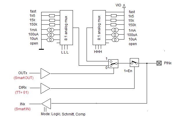
The resistors/current sources are a kind of drive strength. To get a pullup, you need to set the pin to output with a drive strength of 1.5 or 15k or 150k Ohm for HHH and you need to output a High (OUTx=1).
Also if the pin is set to output, you still can read the input.
If the pin is in smartmode, the red labels are valid, DIRx and OUTx do no longer control the IO signals.
Andy
Thanks Andy this is what I was looking for
Regards
Bob (WRD)
Close enough to get the gist. It'll be slightly different, in that OUT/DIR will control the whole mux rather than one switch each.
Here's a logic simulation that works. However, the constant current modes are bogus. It creates a logic error if I try to finish them.
Requires Logisim to run - https://sourceforge.net/projects/circuit/
And a screenshot:
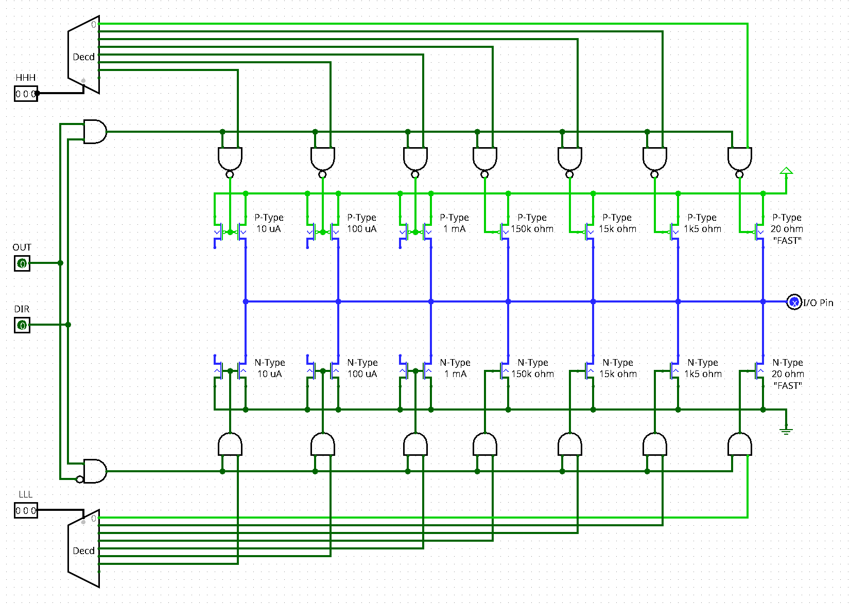
Basically, resistors come free when you get to design each FET. Which is why I've listed the strength of each transistor individually.
Evanh
This is a lot better for clarifying. Hope something like this is put in documents.
Thanks Regards
Bob (WRD)
Just wish Logisim would handle resistors, even in just a logic-only sense.
It may be a basic program but it's quite a nice intuitive program to use. And doesn't crash! That's always handy. I really enjoyed using it earlier - https://forums.parallax.com/discussion/comment/1495168/#Comment_1495168