

SRAM as VGA Buffer
 aaaaaaaargh
Posts: 93
aaaaaaaargh
Posts: 93
in Propeller 2
Hello all,
has anybody done some work on using SRAM as memory for VGA output on the P2 ?
I have seen examples for HyperRam but the P2 has more than enough I/O pins for my purposes, so I'd like to use an IS61WV20488ALL Chip that i've soldered onto a dip adapter. (yes... I know)
It has 16mbit (2Mx8) and has 8ns access time@3.3V.
At first I'd like to be able to display 640x480x8 - ideally 1024x768x8 ot 1280x1024x8 but that is probably to much bandwidth for a dip p2 based system (using Busboard BB3) ?
Any suggestions and or examples would be welcome.
Cheers!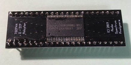
Comments
In theory that can sustain 125 MByte/s fully random mixed read/write. Certainly can't complain about that. A cog by itself could do quite well bit-bashing it.
For linear bursts, using a streamer would be cool but needs thinking if possible. No one has publicly attempted it. There maybe a way to wrangle the smartpins to help with the control signals ...
Address bus is going to be a burden, a cog will be handling that for sure.
I've not looked at SRAM but it might make sense to attempt it. I could probably quite easily create another memory driver that would work with my video driver just like HyperRAM and PSRAM does already. Single Read/writes or read-modify-writes will be straightforward, but bursts require a little more work and would need to involve the streamer for performance. If we can get a COG to drive the address bus while we have the data streamed in or out for reads and writes it could work out. But for speed these addresses probably need to be aligned starting on P0 or P32 if it's being done by a single COG. Then you could just add 1 to porta or portb output register to increment the address in two clocks and get read bursts transferred with something as easy as this. Writes will need a strobe and be slower (at least half the speed).
The 2 P2 clocks per transferred byte works out quite nicely for your 8ns RAM allowing the P2 to run at up to 250-252MHz for VGA resolution over DVI assuming your board's wiring can run data at 125MHz. You'd potentially get truecolour VGA or 16bpp SVGA resolutions or 8bpp for XGA and 8bpp for SXGA, when operating at 200-260MHz.
This could work okay if you place the 3 SRAM control pins on the other output port so the address change doesn't affect them. Or if incrementing always stops at the 2MB boundary and wraps such that the P21 bit doesn't get set it could work. I have burst limits already for another PSRAM type on 4kB boundaries so that likely could be changed to 2MB and that could fix it.
If that method is proven I'd suggest this pin mapping could be used (fully utilizes all of port A):
P0-P20 = A0-A20 address bus for 2MB SRAM (actual connection order doesn't typically matter for SRAM)
P21 = SRAM CS (or on portB)
P22 = SRAM RD (or on portB)
P23 = SRAM WR (or on portB)
P24-P31 = D0-D7 data bus of SRAM (actual connection order doesn't typically matter for SRAM)
Edit: See below for a potential issue.
With additional chip selects and by sharing the address/data bus pins, the memory depth could be increased using my existing bank scheme by connecting more devices. My driver supports up to 16 banks of up to 16MB on a given data bus, or less banks with larger capacity devices. You'll probably run out of pins first though.
Edit: Bear in mind if you use the P2-EVAL or P2 Edge for testing that they have a recently found problem where high speed data on P28-P31 can corrupt the P2 clock timing. If it's your own board design this may not be an issue. e.g. P2D2 and Cluso99's boards don't have this problem. The newer P2-edge should resolve it.
Bit-bashed write (with control pins inverted):
... 'write to SRAM mov outa, addr or outa, sram_write setbyte outa, data, #3 'read from SRAM mov outa, addr 'completes the write cycle, writes are easy bit-bashed or outa, sram_read waitx #8 'wild guess but highlights an issue with bit-bashed getbyte data, ina, #3 ... sram_read long %110<<21 'CE and OE sram_write long %101<<21 'CE and WEHere's first shot at hopefully a working bit-bashed set of routines. Both linear cases are 10 clock cycles per byte. Turns out the sequencing of writes is more complicated than reads, but reads have the Prop2's large I/O latency to overcome.
'
'   IS61WV20488BLL-10WTI  2M x 8 high-speed CMOS Static RAM
'
'   bit31 = /OE Output Enable (low active)
'   bit30 = /WE Write Enable (low active)
'   bit29 = /CE Chip Enable (low active)
'   bit28..08 = A20..0 Address bus
'   bit08..00 = D07..0 Data bus
'

sram_init
        wrpin   ##P_INVERT_OUTPUT, #29 | 2<<6       'config inverted outputs for CE/WE/OE on pins P29/P30/P31 respectively
        mov outa, #0
    _ret_   mov dira, ##$ffff_ff00


sram_wrbyte
        mov outa, sr_addr       'set address bus
        or  outa, srcmd_wr      'start the write operation
        setbyte outa, data, #0      'write data byte to data bus
    _ret_   andn    outa, srcmd_not     'complete the write operation


sram_rdbyte
        mov outa, sr_addr       'set address bus
        andn    dira, #$ff      'tristate the 8-bit data bus
        or  outa, srcmd_rd      'start the read operation
        waitx   #4          'guessed latency compensation
        andn    outa, srcmd_not     'complete the read operation
        or  dira, #$ff      'drive the 8-bit data bus
    _ret_   getbyte data, ina, #0       'read data byte from data bus


sram_wrbytes
        mov outa, sr_addr       'set address bus
        rdfast  #0, hub_addr        'start FIFO

        rep @.rloop, length
        or  outa, srcmd_wr      'start the write cycle
        rfbyte  data            'fetch data from hubRAM block
        setbyte outa, data, #0      'write data byte to data bus
        andn    outa, srcmd_wrn     'complete the write cycle
        add outa, #256      'sr_addr + 1
.rloop
    _ret_   andn    outa, srcmd_not     'complete the write operation


sram_rdbytes
        mov outa, sr_addr       'set address bus
        andn    dira, #$ff      'tristate the 8-bit data bus
        or  outa, srcmd_rd      'start the read operation
        wrfast  #0, hub_addr        'start FIFO

        rep @.rloop, length
        add outa, #256      'sr_addr + 1
        wfbyte  ina         'read data byte from data bus, and write it straight to hubRAM
        waitx   #4          'guessed latency compensation
.rloop
        andn    outa, srcmd_not     'complete the read operation
        or  dira, #$ff      'drive the 8-bit data bus
        wfbyte  ina         'read final data byte from data bus, and write it straight to hubRAM
    _ret_   rdfast  #0, #0          'flush FIFO


srcmd_rd    long    %101<<29        'OE and CE
srcmd_wr    long    %011<<29        'WE and CE
srcmd_wrn   long    %010<<29        'invert WE
srcmd_not   long    %111<<29        'release SRAM
EDIT: Updated sram_init routine.
I see what you did with locating the data bus at the bottom of the 32 bit port. This is potentially useful for single reads/writes as you can wfbyte directly from ina/inb. I guess we can still use the streamer with that connection too and add #256 instead of #1 to the address in the loop which is good. However the address setup needs more shifting up of the address by a byte so it might not save you much in the end, vs a simple getbyte and wfbyte operation. I do think for any video use, you will need to do burst reads with the streamer. Individual access latency will kill you otherwise, especially as it is only byte wide memory to begin with.
For best performance you probably want to hit 125MB/s on burst reads where possible (ie. sysclk/2), and 62.5MB/s for burst writes (sysclk/4). We'll need a smartpin to toggle the WE state at 62.5MHz.
Yeah, I had hoped for better than I got though. The reads could be sped up more but that gets messy real quick and I'm keen to move to trying to get streamer assist going instead.
EDIT: On second thoughts, without hardware to test on, any attempt at the streamer will just be too buggy.
I know, having real HW would make this simple to get going. Maybe I should make up a board to test. I might have some fast ISSI SRAM from another old P1V FPGA project I did.
I'm looking at modifications that would be needed in my PSRAM driver. Reads would be okay to run at this performance, it's only the write fills for words and long sized items that are tricky as you need to change the data AND the address at the same time, so you can't use the streamer to it's full potential. You either need to byte bang the lot or gap the WE clock/strobe between each item (which still might be okay). Write bursts would be more common that doing long fills anyway. A separate byte bang code path for any long and word fills is probably okay to fit in. This is much simpler than the PSRAM was.
If we can strobe the WE pin high on the clock cycle between instructions when outa address and data is stable this byte bang snippet might let us fill longs at the best speed of 62.5MB/s. Filling words would be similar but a shorter loop. We just need to setup the 4 fillbytes ahead of time from the fill pattern. I think this could work out nicely.
rep #8, longfillcount setbyte outa, fillbyte0, #3 add outa, #1 setbyte outa, fillbyte1, #3 add outa, #1 setbyte outa, fillbyte2, #3 add outa, #1 setbyte outa, fillbyte3, #3 add outa, #1Just an idea here but while you could get a cog to increment an address that is port aligned, all that it ends up doing is outputting a "pulse frequency" on the lsb, half that on the next, and so on. You could setup any pins in any order to output that lsb frequency and so on to simulate this "incrementing address" perhaps. Another clock can latch the data from the SRAM.
Optimised the linear read further. Not very confident of its correct timing though. EDIT: Oh, the length for loop cycles is wrong. Still need to add checks and adjustments for that.
sram_rdbytes mov outa, sr_addr 'set address bus andn dira, #$ff 'tristate the 8-bit data bus or outa, srcmd_rd 'start the read operation wrfast #0, hub_addr 'start FIFO add outa, #256 'sr_addr + 1 nop add outa, #256 'sr_addr + 1 rep @.rloop, length add outa, #256 'sr_addr + 1 wfbyte ina 'read data byte from data bus, and write it straight to hubRAM .rloop andn outa, srcmd_not 'complete the read operation wfbyte ina 'read data byte from data bus, and write it straight to hubRAM or dira, #$ff 'drive the 8-bit data bus wfbyte ina 'read data byte from data bus, and write it straight to hubRAM nop wfbyte ina 'read final data byte from data bus, and write it straight to hubRAM _ret_ rdfast #0, #0 'flush FIFONot a bad idea to save the COG some work, but it might take a while to setup all the address pins to different values/phases at the start based on the initial/random memory lookup address. Turns out for 8ns RAM you can't really do it in a single cycle because the WR pulse length needs to be more than 1/2 the clock period. Data sheet for ISSI mentions it as 6.5ns minimum low time, so we'll always need two instructions at the highest P2 speeds to do the write. I was initially hoping we could output the WE pulse at 125MHz but that's too fast. So 62.5MHz would be the next one down.
Ya, I want to rope in using smartpins for anything with a regular pulse time. Or any delayed pulse for that matter ...
I'd be interested to see what happens if we violate that minimum for WE and use 4 ns low time and 4 ns high time from a 250 MHz sysclock. Can still have CE going low earlier, and OE high maintained so there is no turnaround time.
Write data from Prop2 would transition when WE goes low, and the SRAM latching when WE goes high ... is how I see it. I note this also violates minimum tSD = 5 ns though.
We could start off on a slower sysclock to get the bugs out then wind up to 250 MHz.
Yeah you could try to overclock/violate timing but as we know all bets are off then.
LOL, after SRAM the next alternative we can consider is SDRAM. I think it is potentially doable on the P2 as well but it's another major pin burner. 30 pins for 64MB x 8bit wide or 9 more for 16 bit wide. But the memory density is very good and it also transfers up to sysclk/2. The trick would be in the read timing as the read data is really only valid around clock going high, not for the full period. The asynchronous timing delay in the P2 would probably mess this up. There'd need to be some refresh cycles too, possibly using self refresh between accesses and limiting burst sizes.
https://www.issi.com/WW/pdf/42-45R-S_86400F-16320F.pdf
Give this pins some work
I know that you already know this. Unlike SDRAM, The SRAM doesn't require handling refresh. It is easier to read/write. It keeps data without periodic refresh. Hyperram also does this transparently, as well as Pseudo-SRAM. Also, the fact that it is 8ns doesn't means that it must be read/written that fast. It is only the maximum guaranteed allowed operation.
I guess that aaaaaaaargh selected SRAM for this reason (considering how much expensive and lower density this RAM is compared to others). How about some extra small and cheap CPLD/FPGA (ICE40, Altera Max 10M02 ) between the SRAM and Propeller to handle protocol overhead and reduce pin count?
The cheapest and best bang/buck solution is probably 4xPSRAMs with 20 pins used like Parallax are considering for the P2 edge. I was (mostly) only joking about the SDRAM thing. It's hardly worth all the development effort unless you had an application for a massive amount of memory perhaps with lots of paralleled banks sharing the bus. Eg. 256MB could be done with 4 chips.
An FPGA will probably not improve things a lot. Reads can be done at 125MB/s anyway and we have a way to do that by going directly. The only thing it might do is save some pins if they can be multiplexed perhaps, but that will hurt performance a bit.
SRAM is nice for random access if directly coupled to the COG using it. When it is shared by all COGs like my own memory driver does, its read performance comes down into the same ballpark as an 8 bit wide PSRAM setup or HyperRAM running only at sysclk/2. It's just easy to wire in vs HyperRAM BGA if you are doing your own thing, but PSRAM is SOP-8 and is probably even easier to solder vs TSSOP etc.
When you say “8 bit PSRAM setup” are we talking about 2 chips in parallel using SQI Mode?
I had a look at such a setup before getting the SRAM (actually looked at MRAM) but I really thought that this would be a lot slower. I am new to the P2 and I must read up the whole “IO latency” thing... More or less saw me happily bitbanging the thing ;-)
8 bit PSRAM would be 2 chips x 4 bits each. I don't have a driver for that particular configuration but I do have one for 4 chips x 4bits = 16 bits wide, which provides 2x its performance, and quite similar to a single HyperRAM at sysclk/1 rates. The problem with 8 or 16 bit wide PSRAM setup is all the writes need special treatment when not the native storage size of the PSRAM or when they cross 4kB boundaries. I've dealt with all this in my PSRAM driver for a 16 bit bus setup so you don't have to worry about it when you do the mailbox calls...but I can tell you it wasn't easy.
You can bit bang fine when the P2 is slow but as soon as the P2 clock rate starts to increase to higher frequencies the internal I/O latencies start to hit and you need to compensate for this. The read delay needs to be adjusted in different frequency ranges. Writes are usually okay because output clocks/strobes are in already sync with the data so the latency is not typically an issue.
I did a lot with SRAMs on P1.
But the latency on P2 probably means that the P2 is not going to be any faster than P1
for LCD video output there are dedicated chips that have the video ram and LCD packed together.
Only for individual accesses, for burst reads (eg. video) the latency should not be much of an issue with the streamer.
Have the nice SSD1963 based VGA shield from Rayslogic for that :-)
I tried to read back the video ram from the SPI LCDs without success. It was a one-way affair. Every method I tried to read the vram resulted in a lockup of the lcd chip until I issued a reset. While the reset worked without destroying the vram contents, the reset time was unacceptable:(
If anyone finds a way to read back vram, please pm me. I would love to find a way.
FWIW, I could only scroll in one format ie I could only scroll the narrow rows, not the wide rows ie 320 would scroll correctly, but I couldn’t scroll the 480 correctly. So portrait works but not landscape scrolling. Again, pm me if you find a solution.
(pm in case I miss the post)
Under the title I/O PIN TIMING in the prop2 hardware doc But it's mostly just a case of testing each routine and finding out what are the appropriate compensations that work for a given arrangement of instructions.
The root of why it is like this is likely the size of the silicon as much as anything. The internal routes are just so long from cog/streamer to hub to smartpin to pin and all the way back again. The large SRAM blocks push the hub logic a long way from the pins. A major factor is the retaining of high system clock frequency, it required adding extra clocked stages to these long I/O routes. It's something like 4 sysclocks each way when calculating how long an OUT to IN response takes.
But on top of that, when over 80 MHz sysclock there is also an output drive slew time and input propagation time at the pins, or something like that, that comes into play. Adding even more latency. This part is mostly undocumented. Discussed on the forums only.
Better way to apply address to output port to not affect control pins - avoids control pins being negated:
I'm full steam ahead using your REP'd ADD for incremental address generation. It's perfect for sysclock/2.")
Here's my SRAM write loop for bursts under consideration in my driver...it looks something like this. Any clock delays and their positions in the sequence still need to be figured out to line things up, but I think this can work out at the sysclk/4 write rate or 62.5MB/s max for 8ns SRAM.
writecommon setq mask muxq outa, addr1 'get start address of transfer drvl cspin 'activate chip select drvl datapins 'enable the DATA bus setword xsenddata, c, #0 ' setup the streamer transfer length setxfrq xfreq4 'setup streamer frequency (sysclk/4) ' FIX/test if required waitx clkdelay 'odd delay shifts clock phase from data xinit xsenddata, hubdata 'send data from HUBRAM via FIFO waitx clkdelay ' delay might be needed here wypin c, wepin 'start memory clock output on WE pin waitx clkdelay ' or here? rep #2, c 'repeat for bursts nop add outa, #1 'increment address bus call resume 'bursts check what to do next after streaming fltl datapins 'tri-state DATA bus pins _ret_ drvh cspin 'de-assert chip select[incorrect info]
Ok that is good to know. I think it can still work out.