Shop OBEX P1 Docs P2 Docs Learn Events
Prop123 -A9 Testing — Parallax Forums

Prop123 -A9 Testing

cgraceycgracey Posts: 14,133
edited 2015-10-31 02:11 in Propeller 2
After getting the RGB LED problem solved, the -A9 board seems to be working great.

There's a lot to test, but so far, it's running 16 cogs well.

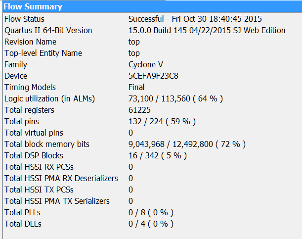
Here's from Quartus:

A9_Compile.png

Here's an exciting movie of all_cogs_blink.spin:

https://drive.google.com/file/d/0B9NbgkdrupkHdjhUU2RRWHA2ejg/view?usp=sharing

Comments

  • Very nice. Congratulations!
  • evanhevanh Posts: 15,290
    16 DSP blocks ... in the CORDIC maybe?
  • cgraceycgracey Posts: 14,133
    evanh wrote: »
    16 DSP blocks ... in the CORDIC maybe?

    The MUL/MLS multiplier in each cog uses a DSP block.

    The CORDIC is nothing more than set of add/subtract stages.

  • evanhevanh Posts: 15,290
    edited 2015-10-31 05:38
    Cool. They'll be subtracted from the used ALM count. Oh, and on that topic, I'd previously come up with a round number of one LE being equivalent to ten gates. If 1 ALM = 1 LE then that implies 700k gates already and Smartpins is still to come!
  • jmgjmg Posts: 15,155
    cgracey wrote: »
    After getting the RGB LED problem solved, the -A9 board seems to be working great.

    What is the build time on that ?
    It seems to have 1M of HUB, does that mean OnSemi can fit more RAM ? ;)

  • cgraceycgracey Posts: 14,133
    jmg wrote: »
    cgracey wrote: »
    After getting the RGB LED problem solved, the -A9 board seems to be working great.

    What is the build time on that ?
    It seems to have 1M of HUB, does that mean OnSemi can fit more RAM ? ;)

    At 180nm, 512KB is all we can fit. The architecture can do 1MB, though, and the -A9 has the RAM, so I had it fill it out.
  • evanhevanh Posts: 15,290
    That one needed no answer. JMG, stop teasing!
  • jmgjmg Posts: 15,155
    edited 2015-10-31 06:44
    evanh wrote: »
    That one needed no answer. JMG, stop teasing!

    hehe, I did have the winky, to show it was not an entirely serious question ;)

  • @ jmg
    It seems to have 1M of HUB, does that mean OnSemi can fit more RAM ?

    You don't need more RAM you just need to learn how to write more efficient code ;)
    Here's an exciting movie of all_cogs_blink.spin:

    Great looking board!!
  • cgraceycgracey Posts: 14,133
    The PLL's work!
  • jmgjmg Posts: 15,155
    cgracey wrote: »
    The PLL's work!

    Can the PLL's be coupled to look like P2 PLLs' for run-time changes, and with the same quantisation ?.
    Or, is the design limited to build-time PLL choices ?
  • evanh wrote: »
    Cool. They'll be subtracted from the used ALM count. Oh, and on that topic, I'd previously come up with a round number of one LE being equivalent to ten gates. If 1 ALM = 1 LE then that implies 700k gates already and Smartpins is still to come!

    ALMs and LEs are not the same. An ALM can do more, but there isn't a simple relationship between the two. I think I read somewhere that you can estimate 1 ALM ≈ 2.5 LE. But the actual number varied considerably based on design and compilation settings.
  • cgracey wrote: »
    jmg wrote: »
    cgracey wrote: »
    After getting the RGB LED problem solved, the -A9 board seems to be working great.

    What is the build time on that ?
    It seems to have 1M of HUB, does that mean OnSemi can fit more RAM ? ;)

    At 180nm, 512KB is all we can fit. The architecture can do 1MB, though, and the -A9 has the RAM, so I had it fill it out.

    For testing purposes, please keep it at 512K.
  • RaymanRayman Posts: 14,065
    I don't know... This is a great marketing feature for P123 board.

    Even after the P2 chip comes out, somebody who needs more RAM might spring for a P123 board...
  • RaymanRayman Posts: 14,065
    What are the pin assignments for the SDRAM ?
  • Great news Chip :D
  • Maybe when there is time for a breather, a 512K "for real" build can be done.

    I wonder about JMG's question too. If the PLL is working, can we modify the clock?

  • cgraceycgracey Posts: 14,133
    In my experience, to get an Altera PLL to feed from an NCO, the only way to do it is to output the NCO on a pin and then input it on another to feed the PLL. Quartus is very picky like that.

    You can reconfigure PLLs at run-time, but you need to feed them a configuration bitstream. Not simple.
  • Ok, no worries.
  • LoopyBytelooseLoopyByteloose Posts: 12,537
    edited 2015-10-31 16:05
    Well using 132 of the 224 pins available on the A9 indicates that the BeMicroCVA9 will never provide complete i/o emulation. It has only 102 i/o pins available.

    So it looks like the P123 A9 is a must for complete emulation. Happy to see the P123 A9 is coming along.
  • May I tag my name on the list for an A9 board if there is one available after the 'regular' crew have theirs?
  • I assume that the A7 board will continue to be supported even after the A9 board is available? Is that correct?
  • cgraceycgracey Posts: 14,133
    David Betz wrote: »
    I assume that the A7 board will continue to be supported even after the A9 board is available? Is that correct?

    Yes.
  • jmgjmg Posts: 15,155
    Seairth wrote: »
    For testing purposes, please keep it at 512K.

    Both are useful to have.
    Certainly, for final FPGA testing, whatever the P2 chip will have ( which may not be exactly 512k) should be used.

    !M is still useful to test, to fully confirm the Opcode reach, as OnSemi might come back and say 580k of RAM can fit.

    Plus, as other mention, it is a useful FPGA-only target
    In fact, the FPGA can support more than that.
  • jmgjmg Posts: 15,155
    cgracey wrote: »
    In my experience, to get an Altera PLL to feed from an NCO, the only way to do it is to output the NCO on a pin and then input it on another to feed the PLL. Quartus is very picky like that.

    You can reconfigure PLLs at run-time, but you need to feed them a configuration bitstream. Not simple.

    hmm.. Less than ideal, but I suppose partial config may allow a selection of PLL settings to be tried, via a few small PLL_Setting files ?

    I also find
    https://www.altera.com/content/dam/altera-www/global/en_US/pdfs/literature/an/an661.pdf

    which shows an ALTERA_PLL_RECONFIG IP Core, but that does not look seamless either.

    I note that A9 has 8 PLL's so an alternative approach could be to choose some useful defaults for multiple PLLs and then select which to use (Assuming that can be a run-time choice?)
  • pedwardpedward Posts: 1,642
    edited 2015-11-03 22:27
    640k 512k should be enough for anyone.

    The question is, since 130nm was the tick for 180nm's tock, does OnSemi offer 130nm with the same features as 180nm, then allowing for 1MB of RAM?

    EDIT: I looked and their next step is 110nm. What's very interesting, aside from 3.3v and 5v tolerance is that the power dissipation at 110nm is 9nW per Mhz per gate and it's 46nW per Mhz per gate in 180nm! That's 5 times less power dissipation!

    One downside is that 180nm is considered their 'low price' solution while 110nm is not.
  • cgraceycgracey Posts: 14,133
    edited 2015-11-04 00:14
    pedward wrote: »
    640k 512k should be enough for anyone.

    The question is, since 130nm was the tick for 180nm's tock, does OnSemi offer 130nm with the same features as 180nm, then allowing for 1MB of RAM?

    EDIT: I looked and their next step is 110nm. What's very interesting, aside from 3.3v and 5v tolerance is that the power dissipation at 110nm is 9nW per Mhz per gate and it's 46nW per Mhz per gate in 180nm! That's 5 times less power dissipation!

    One downside is that 180nm is considered their 'low price' solution while 110nm is not.

    I wonder how much more expensive it is. I will ask them, for whatever it's worth, at this point.

    Update... I went and looked at their site to see what technologies are offered today and they only go down to 180nm, in house. They outsource those other technologies. We talked to them once about 65nm, but it was going to be over half a million to get it done. I think we need to just finish this at 180nm and then see what we can do, after that.
  • RaymanRayman Posts: 14,065
    Still thinking about that low cost digital only option? What was it, $60k or so...
  • pedward wrote: »
    EDIT: I looked and their next step is 110nm. What's very interesting, aside from 3.3v and 5v tolerance is that the power dissipation at 110nm is 9nW per Mhz per gate and it's 46nW per Mhz per gate in 180nm! That's 5 times less power dissipation!

    One downside is that 180nm is considered their 'low price' solution while 110nm is not.

    I worked at ASML when they were developing the 180nm lithography machines in 1999. Those machines use Deep Ultraviolet lasers (DUV) to project the chip patterns onto a wafer through a gigantic lens. To get better resolutions, you need shorter wavelengths of light (such as EUV -- Extreme Ultraviolet) which get absorbed by pretty much everything so current machines use a vacuum and mirrors instead of air and a lens.

    So yeah, going to a better resolution is not just a matter of adjusting some knobs and running the wafer a little slower or something. They have to use different machines and apparently OnSemi doesn't have those.

    ===Jac
Sign In or Register to comment.