

SX20 in a 14 Pin DIP
 Bean
Posts: 8,129
Bean
Posts: 8,129
I have a lifetime supply of leadframes on order. So I'm looking for projects to use them.
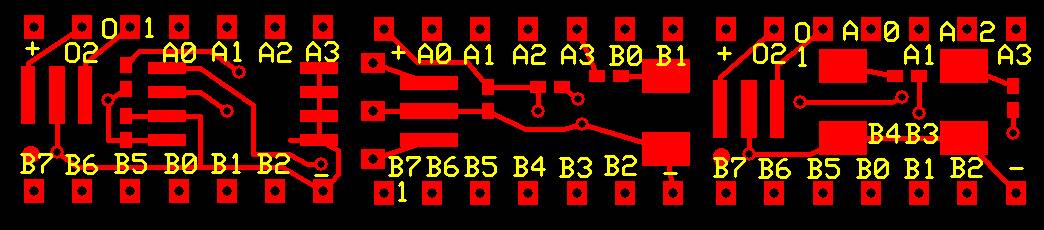
What do you think about an SX20 in a 14 pin DIP package ?
The SX20 is on the bottom to allow for labels for the pins.
Note that A3 is also connected to RTCC, so you can use that pin for either or.
EDIT:
· I·have changed it to try to get RB.0, RB.1, and RB2 so you can use the comparitor.
··I also added the pull-up resistor for·MCLR and a by-pass cap, so you can use it to make a stand-alone device.
EDIT2:
· I have made three versions.
··· One with 2 LEDs on-board.
··· One with a 128KB EEPROM on-board.
··· One with the OSC pins on the edge (all I/O connected to pins).
Bean.
·
▔▔▔▔▔▔▔▔▔▔▔▔▔▔▔▔▔▔▔▔▔▔▔▔
- - - - - - - - - - - - - - - - - - - - - - - - - - - - - - -
www.iElectronicDesigns.com
Post Edited (Bean (Hitt Consulting)) : 12/2/2007 4:22:54 PM GMT
1044 x 230 - 54K
1053 x 226 - 60K
Comments
Robert
regards peter
▔▔▔▔▔▔▔▔▔▔▔▔▔▔▔▔▔▔▔▔▔▔▔▔
DTQ
I am curious to know why you did not bring all of the Port B pads out to pins but chose, instead, to bring three Port A pads out to pins. I can see an advantage to being able to use byte operations to affect all eight Port B signal pins at a time. You might have seen more of an advantage to bringing out three of the Port A pins. Was this to make it easier to support I2C, SPI, chip select and enable pins, etc. from a separate port? If so, I guess I do not see that as a significant advantage.
Also, I do not see the logic in breaking up the Port B pins into two separate groups of three pins. I think a consecutive grouping would be a better option. I am wondering why you chose this configuration.
I hope it does not seem like I am criticizing your design decisions. I am only seeking to understand your thought process with the hope that I may learn something I have not previously considered.
I think a 14-pin version could be useful. (I am not sure how small the market might be.) However, it sounds like there is a bit of a cry for an 18-pin version. Heed the cry!
- Sparks
I simple choose the pins and the order that could be connected the easiest. [noparse];)[/noparse]
The 14 pin version was to allow me (and others) to sell programmed chips that do certain functions (PWM, Servo control, ect). So it has a by-pass cap, and /MCLR pulled up with a 47K resistor. Basically a plug in and go controller.
I'm working on a SX18 version, seems like there is demand for it. But it won't be nearly as cheap as an SX18 chip.
Bean
▔▔▔▔▔▔▔▔▔▔▔▔▔▔▔▔▔▔▔▔▔▔▔▔
- - - - - - - - - - - - - - - - - - - - - - - - - - - - - - -
www.iElectronicDesigns.com
·
Here is my design for a dip18. It is a tight fit. All traces are 12mil, pads are 60x40mil hole 28mil.
Vias are diameter 40mil, hole 20mil. The chip goes to the bottom side.
regards peter
Wow that certainly is nicer than the mess I've been working on.
Nice job.
Bean.
▔▔▔▔▔▔▔▔▔▔▔▔▔▔▔▔▔▔▔▔▔▔▔▔
- - - - - - - - - - - - - - - - - - - - - - - - - - - - - - -
www.iElectronicDesigns.com
·
so I will not get these boards manufactured.
If you want I can send you the gerber files.
regards peter
That's quite an elegant layout! Nicely done!
-Phil
Peter, I agree with others -- an elegant layout for an 18 pin design.
▔▔▔▔▔▔▔▔▔▔▔▔▔▔▔▔▔▔▔▔▔▔▔▔
Tracy Allen
www.emesystems.com
I do agree about not have the /MCLR pin though. I have added the MCLR pull-up (47K), a 0.1uF by-pass cap and a 20MHz resonator pads.
So now there are 10 I/O pins, and you can still use RTCC (on RA.3), and the comparitor (RB.0, RB.1, RB.2).
I have updated the pictures in the first post.
The board is 0.350" high, so I'll have to bend the leadframes in slightly to get the 0.300" width. I just couldn't get it connected at 0.300".
[noparse][[/noparse]Edit] Oops, found out that the leadframe clips will hit the SX package. Darn, I had to increase the·heigth to 0.390", well at least that gives me more room . I want to make two versions, one will use the 2 unused pins for·on-board red and green LEDs. The other will have an on-board I2C EEPROM.
Bean
▔▔▔▔▔▔▔▔▔▔▔▔▔▔▔▔▔▔▔▔▔▔▔▔
- - - - - - - - - - - - - - - - - - - - - - - - - - - - - - -
www.iElectronicDesigns.com
Post Edited (Bean (Hitt Consulting)) : 12/2/2007 3:31:23 AM GMT
Would the chip interfere with the leadframe if it were on the top instead of on the bottom? Having silk-screened pin labels on top seems less important, and could be printed on a paper overlay.
How about putting 2 holes on the end next to the resonator for programming/debug via a small header? I'm not letting up on the two clock pins, that could be used to get all 12 i/o to the outside.
▔▔▔▔▔▔▔▔▔▔▔▔▔▔▔▔▔▔▔▔▔▔▔▔
Tracy Allen
www.emesystems.com
· The leadframe connects to both the top and the bottom, so it wouldn't matter.
· I made the board larger, and have 3 versions. One has 2 LEDs on the unused pins, one has a 128KB EEPROM on the unused pins, and one has all the I/O pins with the OSC pins on the end.
· It's going to be a chore to bend the leadframes, but this is the first revision maybe I'll think of something clever later.
· I have updated the pictures in the first post.
Bean
▔▔▔▔▔▔▔▔▔▔▔▔▔▔▔▔▔▔▔▔▔▔▔▔
- - - - - - - - - - - - - - - - - - - - - - - - - - - - - - -
www.iElectronicDesigns.com
Post Edited (Bean (Hitt Consulting)) : 12/2/2007 4:23:22 PM GMT
Are you talking about the kind of lead frame you see on the BASIC Stamp modules, that wrap around the side of the board? Those do take a a lot of space. And it would be a royal pain to have to bend it in to fit 0.3"!
I was thinking more in terms of PC pins, like the ones from Mill-Max. Some of them fit through a 0.020 hole and take only a 0.030 pad. Maybe Peter's SX18 design was planned around something like that? It is a bit of a pain to load the pins with good alignment, but it can be done pretty quickly with a simple alignment jig.
I'm attaching my try at a 14 pin layout with the resonator next to the SX20 and the clock pins at the end for programming. The SX20 and resonator are on the top, and the mclr pullup and bypass cap are on the bottom. The pins CCW from lower left are B0, B1, B2. B3, B4, B5, B6-- X2, X1 --B7, V+, A0, A1, A2, A3, V-.
▔▔▔▔▔▔▔▔▔▔▔▔▔▔▔▔▔▔▔▔▔▔▔▔
Tracy Allen
www.emesystems.com
Bean, attached is a 8pin dip design. Pins available are B0-B3, where B3 is also connected to RTCC.
Also added pullup for MCLR and pads for onboard oscillator/resonator
(I estimated oscillator pad sizes from your drawings).
Edit: added a version 3, with onboard cap and sxkey connection.
The idea is to have two 4x1 pinheaders on bottom·for insertion into DIP8 socket
and one·4x1 pinheader on top for sxkey.
Edit: added a version 4, removed OSC1, OSC2 and RB3 pins, added RA0, RA1 and RA2 pins.
Edit: added an alternative bottom layer to V4, where RA2 connects to RTCC (instead of RA3)
Edit: added a version 5 that has VDD and VSS pins changed to match EEPROM socket.
regards peter
·
Post Edited (Peter Verkaik) : 12/4/2007 9:01:58 PM GMT
▔▔▔▔▔▔▔▔▔▔▔▔▔▔▔▔▔▔▔▔▔▔▔▔
Tracy Allen
www.emesystems.com
Post Edited (Tracy Allen) : 12/4/2007 7:24:08 AM GMT
you should consider using 4-layer boards with two inner supply layers, one connected to Vdd, and the other to Vss. This makes routing of the power signals much easier, and adds a nice "filter cap" against EMI. At least here in Germany, the price difference between two- and four layer boards is not that much. I'm using this technique for most of my new designs.
▔▔▔▔▔▔▔▔▔▔▔▔▔▔▔▔▔▔▔▔▔▔▔▔
Greetings from Germany,
G
Guenther, I wish ExpressPCB had an inexpensive 4 layer option. I would definately use it.
Bean
▔▔▔▔▔▔▔▔▔▔▔▔▔▔▔▔▔▔▔▔▔▔▔▔
- - - - - - - - - - - - - - - - - - - - - - - - - - - - - - -
www.iElectronicDesigns.com
·
(see V4 attachement of my previous post). I was thinking RA3 connected to RTCC would
allow·to induce an interrupt without altering available I/O pins, the same
can however also be done by toggling an unused RB pin.
regards peter
You can induce an interrupt with any of the unused RB pins.
RTCC is most useful in counting an external signal (if you use the RTCC prescaler you can count a signal many times faster than the SX clock).
It's amazing how many cool DIP units can be made. I have order boards and they will be here Friday. Now if only I had my reel of leadframes I ordered....Argg...
Bean
▔▔▔▔▔▔▔▔▔▔▔▔▔▔▔▔▔▔▔▔▔▔▔▔
- - - - - - - - - - - - - - - - - - - - - - - - - - - - - - -
www.iElectronicDesigns.com
·
▔▔▔▔▔▔▔▔▔▔▔▔▔▔▔▔▔▔▔▔▔▔▔▔
There's nothing like a new idea and a warm soldering iron.
Here is my smallest 8 pin DIP layout. Pins 1 & 8 will have to extend above and below the PCB. SX-Key connects to the 4 pins down the right side.
A3 (pin 6) is also RTCC, and OSC1(pin 8) can be used with an external clock or an external RC circuit.
Bean
▔▔▔▔▔▔▔▔▔▔▔▔▔▔▔▔▔▔▔▔▔▔▔▔
- - - - - - - - - - - - - - - - - - - - - - - - - - - - - - -
www.iElectronicDesigns.com
I see what you are saying about the easier layout wit 4 layers. But the price here can be pretty steep for prototypes or short runs. Not too much for production though.
I have a couple of questions for you about your 4 layer layouts, Where do you leave your exclusion areas, if any? For example, the X1 pin is sensitive, as are areas around a high speed input for something like sigma-delta. In a general purpose design it is hard to predict what each pin will be used for. and if a few extra pF to ground will be bad.
As to EMC, how important do you think the 4 layer layout is for meeting CE guidelines?
▔▔▔▔▔▔▔▔▔▔▔▔▔▔▔▔▔▔▔▔▔▔▔▔
Tracy Allen
www.emesystems.com
I uploaded a version 5 (see my earlier post) that has VDD and VSS pins changed
to match EEPROM socket.
regards peter
too bad to hear that prices for 4-layer prototypes are that much higher in the US than here.
Actually, I usually don't leave any exclusion areas. You are right that the two inner layers add some capacitive load to signal traces on the top and bottom sides of the board. Although I made no measurements so far, I guess that such short and thin traces can only build up a minimum capacitive load against the nearest inner layer in an area of some pF at maximum. When you consider that a ceramic resonator attached to the X1 pin usually has a built-in capacitor of several pF between X1 and Vss, the additional trace capacitance can be almost ignored. The same is true for high-speed inputs for sigma-delta. Here, you usually have a capacitor of 0.1 µF between the input and Vss, and the same capacitor with 10 kOhm in series between the output. So, I think the additional "stray capacity" between the traces and the inner layers can be ignored again.
IMO, the few extra pF between inputs and ground don't cause any trouble but - on the other hand - help to reduce generated EMI.
When I did my first commercial SX-based hardware designs with SXes clocked at 50 MHz, I got in deep trouble when I had those boards checked for EMI conformity. It turned out that most of the EMI was generated by the supply traces, and the "filter caps as close as possible between the supply pins"-trick did not really work. After switching to the 4-layer design, the EMI problems were gone.
There was a thread in this forum section regarding EMI a long time ago - unfortunately, it is older than one year, so I could not find it using the forum's search function.
▔▔▔▔▔▔▔▔▔▔▔▔▔▔▔▔▔▔▔▔▔▔▔▔
Greetings from Germany,
Günther
I reworked your DIP8 design to have pins A0/RTCC, A1, B0, B1 and B2.
If you ever do a dip8 version, this is my favourite.
regards peter