@jmg said:
How do they connect the middle DIP pins ?
If you assemble manually you could trim some of the pins down, drill only partly into the bottom of the board or maybe fold the pin at right angles, solder them underneath and then push these header pins back through black plastic strip. I've resorted to that type of approach a couple of times in the past for fixing something, but it was certainly a manual process and wasn't too secure. This might be better because there are some extra pins on each side to strengthen it.
The mouse-bites suggest this was a proof-of-concept, and manually the headers could be trimmed and hand-soldered like that.
Moving to production manufacturing would require deep pockets! Custom header, custom soldering process, etc...
The headers could be ordered with the tails for those center pins shorter than the rest - perhaps just 1mm to go into a PCB that's been drilled through on all but the outer-most 1 or 2 layers for the uC. So far not a huge issue; least not that money can't solve with the right MOQ.
Using pre-loaded solder, or solder-in-pad, they could be installed prior to reflow. (Though I can't see in the photo angle, it doesn't look like the headers used have the risers for reflow soldering; another clue toward prototype build!)
The longer tails will provide sufficient mechanical strength, so header-wise all good like that- just expensive to setup the process. Would need a special (super fine) selective soldering nozzle to hit those TH header pads right beside the uC corner pins too! $$$! Or again, a clue that hand soldering was used there.
And then to consider a second reflow pass, due to the double-sided SMT. Perhaps the XILINX goes on last with lower-temp solder paste. That way, those TH headers could have been run through a more bog-standard selective soldering process first, with higher temp LF solder. (Which demotes the previous point somewhat- maybe like this, it wouldn't be so tough to manufacture. Just the solder-in-pad on the middle 8 or so pins would need some care).
Goodness- would really be a fantastic engineering challenge to put all the pieces together on bringing that to production. Great opportunity. Hmm... Next time I'm chatting with Parallax manufacturing I know what the topic will be !!
Mind whirring... if we could make a P2 module like that... would that be the form-factor to sell 1000's ?
And... Would having thermal limitations be an impediment to sales ? -- Could recommend (and stock) a suitable fan I suppose, for overclocked applications.
Assuming USB-C, ,maybe Bluetooth, maybe mini-HDMI socket, and maybe some PSRAM. (and maybe microSD 4-bit based on evanh research; ie. not on the boot pins).
Compared to Edge form-factor for mass uptake and system-builder usage, is there such a difference here? I wonder if the DIP form-factor is more suited to attract first-time dabblers, where-as the edge module is perhaps "better" for system builders; especially with it's thermal advantages and access to all the I/Os.
Comparison could lead to both as good options - one form-factor might encourage/unlock new uptake, even if future products/projects might be designed around the other module.
During P2LF you mentioned the castellated option... How would you see the power supply/requirements ?
Maybe a 3.3V powered module, which would supply all the VIOs from the user power source, and on-board 1.8V regulation for the P2 core?
That would save the space around the chip being used by the 3.3V LDOs at the moment. We'd need to fit a larger 1.8V regulator, plus the XTAL I suppose.
Would you want boot memory on board? Or just let the user add their own external flash or uSD (or serial) connection ?
And what about max operating frequency? ... Though "if" the bottom side of the module could be kept empty and with a solid exposed (un-masked) ground plane, then the user could ensure suitable thermal pathways onto their own board.. would that work for the application you had in mind?
Wow, thanks for that link @TonyB_
I'm amazed by the price, and it seems they "must" be hand-rolling them to some extent. I suspect without a major marketing injection, we couldn't get close to that price with a P2 module.
During P2LF you mentioned the castellated option... How would you see the power supply/requirements ?
Maybe a 3.3V powered module, which would supply all the VIOs from the user power source, and on-board 1.8V regulation for the P2 core?
That would save the space around the chip being used by the 3.3V LDOs at the moment. We'd need to fit a larger 1.8V regulator, plus the XTAL I suppose.
Would you want boot memory on board? Or just let the user add their own external flash or uSD (or serial) connection ?
And what about max operating frequency? ... Though "if" the bottom side of the module could be kept empty and with a solid exposed (un-masked) ground plane, then the user could ensure suitable thermal pathways onto their own board.. would that work for the application you had in mind?
These are great questions. What I'm thinking is a square, like the center of the edge board with castellated pins all around.
Maybe having 1.8 V regulators there instead is good, I don't know.
If that doesn't change the max. freq of the chip, that'd be fine.
It could be bigger if that meant adding in the 1.8 regulators and the clock source.
Definitely not the boot memory or uSD.
Max operating frequency is the main goal for me. Was just thinking about how to do the bottom...
Is it better open? Or, better to have an array of vias to ground plane on a 2 layer host PCB?
IDK... Either way is fine by me though...
General idea is to get the thermal performance of the edge using a 2-layer host board...
It could also be that it's not thermal at all, but having those caps very close to the pins.
Not 100% sure why edge is better than my 4-layer boards (in terms of reliable max. freq)...
About the tiny black regulators and associated caps on the current Edge boards (as per your cropped photos)- those are all the 3.3V VIO regulators, one per group of 8 IOs.
If we removed them, we'd have more space to make other sensible choices.
We couldn't just replace the 3.3V LDOs with 1.8V LDOs for the core, as the core would need one consistent voltage level (not multiple regulators with slight variation). So it means a larger package 1.8V on the board somewhere. But even so, it need not be so big that the castellated module gets so much bigger, and we could use some of the space saved by the 3.3V LDO removal to some extent.
I think having the 1.8V onboard is rather compelling, so that the module would run completely from a 3.3V supply.
For the thermal pad, it would be better on the castellated to be open, and then you have a matching open area on your 2 -layer board, and probably a "wipe" of heatsink compound, or a thermal "sticker".
You'd certainly do better with a good array of vias on your 2-layer board if you have a ground plane on the second side, to help get heat away anywhere you can!
This is an interesting question, to make a castellated module that relies on a host to provide the boot memory and most everything else. Not that those things in themselves are such an issue, but the thermal limits of shrinking the copper would need to be explored; as would the placing (or space to place) all the traces, gnd and signal-gnd return vias. Would probably take a few days of design effort even to get to the point of knowing with some confidence if (or how) it could work, and how many layers would be needed.
And then with it being finished, would it be the sort of things that many customers could use? I'm thinking about the lack of boot mostly, and wonder if it should at least have a small boot flash on-board? hmm.. mind you, it would certainly need special layout on the user board anyway. Pros/Cons
What would the user-board look like..... 3.3V regulator, perhaps 4 or 5 Amp. Boot device (flash or uSD). Serial header for PropPlug. Wow, maybe that's all. Not so much- excluding the user application stuff of course. Ideally the user board would have a solid copper area to "mate" with the bottom of the castellated module, and have plenty of vias through to the bottom side of the user board, which would ideally also be a solid ground plane (or at least plane to the edges of the PCB on at least 2 edges). That puts all the user signal traces on the top side- maybe not an issue. Except the bigger problem there is high-speed integrity, as the ground plane on a 2-layer board is "miles away". So much will depend on intended application.
@Rayman said:
General idea is to get the thermal performance of the edge using a 2-layer host board...
It could also be that it's not thermal at all, but having those caps very close to the pins.
Not 100% sure why edge is better than my 4-layer boards (in terms of reliable max. freq)...
What about using an Edge module socket on your 2-layer board? Does that reach your intended goal? (OR at least well enough that it makes sense to avoid the time and hardware cost of building something new whilst you're experimenting?). -- sorry, you might be passed that stage- I'm assuming recklessly!
Speculation to your points:
The thermal thing wouldn't impact signal integrity in that way - ie. max freq. limitation - At least, not until it properly overheats and starts to shut-down, which would then happen obviously quickly.
More likely another issue, or combination. Could be compromised signal-gnd return paths, could be the caps if they are not located and wired in optimally enough to prevent the sort of voltage level oscillations that are sufficient to degrade your signal to the point that they cannot operate faster than X. Both those things are certainly amplified at higher frequency. ie. The odd voltage dip here and there, at nS speeds could be unintendedly shifting the logic threshold, such that 1 might be read as 0 at the wrong moment, forcing your application to limit max freq. Same applies to the choice of XTAL and the layout around that.
I'd be fine with whatever can be done. Thinking you probably know better.
Regulators on the host board would be just fine. Maybe even better for the 3.3 V to be on the host board, so can be tailored for the particular application...
Having the 1.8 V regulators on this "core" board would be fine and maybe make sense, but doesn't need to be.
Really just want reliable 350+ MHz operation, like see with Eval and Edge...
The edge can work for some of my applications, but not others.
This "core" thing would allow more flexibility in design...
Also, just generally like hard soldered connections.
Personally, not a fan of the shared uSD/flash and the dip switches. It just makes things too complex, IMHO.
Also, seems we now have a 4-bit uSD driver, thanks to @evanh, so most likely implementing that in future boards...
My boards do OK with 4 layers, all can do 320 MHz and about half can do 340 MHz.
But, the edge can do a lot better, and I'd like to get there.
Also, soldering the P2 is something that I can do, but it's not always easy.
This would make it a lot easier for me to assemble boards, I'm thinking...
@Rayman said:
Personally, not a fan of the shared uSD/flash and the dip switches. It just makes things too complex, IMHO.
Agree with that! Mega pain! Though for demo, to allow a choice, it was efficient with IOs I suppose.
Moving to a customer application, I'd sure want to target just one boot path also; for reliability at least, if not simplicity.
Guess would be interesting if this "core" thing could also be soldered onto a DIP layout to form something similar to what @TonyB_ showed...
Not really my thing, but seems might be interest...
@evanh said:
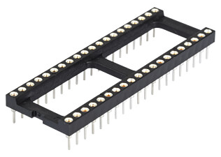
Good trick making the IC sit right on the DIP pins like that. I can only assume those few DIP pins are surface mounted underneath. Would need a very custom library part, or maybe done with three end-to-end DIP socket parts instead.
You can SMT/reflow solder one of these IC sockets to the bottom.
There are 2 problems though:
1. make sure it's made of glass fibre reinforced plastic. The standard plastic melts in the oven.
2. there are no centering pins so it has to be aligned carefully
However, mechanical strength is much better than with single row pin headers. So even if this doesn't have THT pins it should be strong enough to withstand push/pull in/out of breadboards.
@evanh said:
Good trick making the IC sit right on the DIP pins like that. I can only assume those few DIP pins are surface mounted underneath. Would need a very custom library part, or maybe done with three end-to-end DIP socket parts instead.
You can SMT/reflow solder one of these IC sockets to the bottom.
There are 2 problems though:
1. make sure it's made of glass fibre reinforced plastic. The standard plastic melts in the oven.
2. there are no centering pins so it has to be aligned carefully
However, mechanical strength is much better than with single row pin headers. So even if this doesn't have THT pins it should be strong enough to withstand push/pull in/out of breadboards.
I've sharpened the bottom view of the vla82:
It seems that two continuous 20-pin strips were used as I can't see any joins. From side views there is small gap between bottom of PCB and top of black pin strip material.
@TonyB_ said:
I've sharpened the bottom view of the vla82:
It seems that two continuous 20-pin strips were used as I can't see any joins. From side views there is small gap between bottom of PCB and top of black pin strip material.
The first image looked to have square pin, the second one uses machine pins.
It looks like most pins are thru-hole, so they could use a snip-and-file* approach for those few inner pins and then a reflow pass.
We use snip-and-file on volume production, it's tolerable when there is no alternative, and if the volume hits 10,000's I'm sure a connector supplier can roll something, at a price.
A minus with machine pins, is the ease of breaking.
lcsc have these in stock, the top side has a decent shoulder for soldering.
*If the board used blind-via, ($$) you could perhaps skip the file step, as the cut-off has a small hole to poke into.
I have been reading all these comments on a new P2 module product. and it is all well and good.
I may be an outlier type person, but my one and ONLY design & fabrication concern is: When China invades Taiwan, all of this stuff you talk about will disappear. You won't be out of business in a Month, a Week or a Day, you will be out of business in an Hour.
We, all of us, need to bring it all home.
End of rant.
Below are two side views of the underside of a vLA128, another ZX Spectrum ULA replacement. Reminder: this is a 40-pin DIP with a CPLD on top that has same package as the P2. Five pins either side do not pass through the PCB because the CPLD is in the way. Can anyone work out how from the photos how these ten pins are soldered? To me, it looks like there are solder pads next to these pins.
I have said this before, but y'all not listening...
No friend of CHINA... When China (not if) invades Taiwan, all this stuff, components like resistors, caps, connectors, transistors... will disappear overnight. I have long abandoned "Lean" manufacturing for "Adaptive" manufacturing; something like SMD pads that support both 0805 and 0603, and other active & passive parts.
As for "Must Have", and "Nice to Have" ... Choose wisely. End of rant.


Comments
If you assemble manually you could trim some of the pins down, drill only partly into the bottom of the board or maybe fold the pin at right angles, solder them underneath and then push these header pins back through black plastic strip. I've resorted to that type of approach a couple of times in the past for fixing something, but it was certainly a manual process and wasn't too secure. This might be better because there are some extra pins on each side to strengthen it.
I was thinking similar to rogloh.
The mouse-bites suggest this was a proof-of-concept, and manually the headers could be trimmed and hand-soldered like that.
Moving to production manufacturing would require deep pockets! Custom header, custom soldering process, etc...
The headers could be ordered with the tails for those center pins shorter than the rest - perhaps just 1mm to go into a PCB that's been drilled through on all but the outer-most 1 or 2 layers for the uC. So far not a huge issue; least not that money can't solve with the right MOQ.
Using pre-loaded solder, or solder-in-pad, they could be installed prior to reflow. (Though I can't see in the photo angle, it doesn't look like the headers used have the risers for reflow soldering; another clue toward prototype build!)
The longer tails will provide sufficient mechanical strength, so header-wise all good like that- just expensive to setup the process. Would need a special (super fine) selective soldering nozzle to hit those TH header pads right beside the uC corner pins too! $$$! Or again, a clue that hand soldering was used there.
And then to consider a second reflow pass, due to the double-sided SMT. Perhaps the XILINX goes on last with lower-temp solder paste. That way, those TH headers could have been run through a more bog-standard selective soldering process first, with higher temp LF solder. (Which demotes the previous point somewhat- maybe like this, it wouldn't be so tough to manufacture. Just the solder-in-pad on the middle 8 or so pins would need some care).
Goodness- would really be a fantastic engineering challenge to put all the pieces together on bringing that to production. Great opportunity. Hmm... Next time I'm chatting with Parallax manufacturing I know what the topic will be !!")
Mind whirring... if we could make a P2 module like that... would that be the form-factor to sell 1000's ?
And... Would having thermal limitations be an impediment to sales ? -- Could recommend (and stock) a suitable fan I suppose, for overclocked applications.
Assuming USB-C, ,maybe Bluetooth, maybe mini-HDMI socket, and maybe some PSRAM. (and maybe microSD 4-bit based on evanh research; ie. not on the boot pins).
Compared to Edge form-factor for mass uptake and system-builder usage, is there such a difference here? I wonder if the DIP form-factor is more suited to attract first-time dabblers, where-as the edge module is perhaps "better" for system builders; especially with it's thermal advantages and access to all the I/Os.
Comparison could lead to both as good options - one form-factor might encourage/unlock new uptake, even if future products/projects might be designed around the other module.
@Rayman
During P2LF you mentioned the castellated option... How would you see the power supply/requirements ?
Maybe a 3.3V powered module, which would supply all the VIOs from the user power source, and on-board 1.8V regulation for the P2 core?
That would save the space around the chip being used by the 3.3V LDOs at the moment. We'd need to fit a larger 1.8V regulator, plus the XTAL I suppose.
Would you want boot memory on board? Or just let the user add their own external flash or uSD (or serial) connection ?
And what about max operating frequency? ... Though "if" the bottom side of the module could be kept empty and with a solid exposed (un-masked) ground plane, then the user could ensure suitable thermal pathways onto their own board.. would that work for the application you had in mind?
Here's a view of the underside of the PCB (image unsharpened):

(The cable connects to a YUV to RGB converter.)
Various ULA, gate array and audio IC replacements available:
https://www.vretrodesign.com/collections/product-catalog?page=2
Wow, thanks for that link @TonyB_
I'm amazed by the price, and it seems they "must" be hand-rolling them to some extent. I suspect without a major marketing injection, we couldn't get close to that price with a P2 module.
These are great questions. What I'm thinking is a square, like the center of the edge board with castellated pins all around.
Maybe having 1.8 V regulators there instead is good, I don't know.
If that doesn't change the max. freq of the chip, that'd be fine.
It could be bigger if that meant adding in the 1.8 regulators and the clock source.
Definitely not the boot memory or uSD.
Max operating frequency is the main goal for me. Was just thinking about how to do the bottom...
Is it better open? Or, better to have an array of vias to ground plane on a 2 layer host PCB?
IDK... Either way is fine by me though...
General idea is to get the thermal performance of the edge using a 2-layer host board...
It could also be that it's not thermal at all, but having those caps very close to the pins.
Not 100% sure why edge is better than my 4-layer boards (in terms of reliable max. freq)...
About the tiny black regulators and associated caps on the current Edge boards (as per your cropped photos)- those are all the 3.3V VIO regulators, one per group of 8 IOs.
If we removed them, we'd have more space to make other sensible choices.
We couldn't just replace the 3.3V LDOs with 1.8V LDOs for the core, as the core would need one consistent voltage level (not multiple regulators with slight variation). So it means a larger package 1.8V on the board somewhere. But even so, it need not be so big that the castellated module gets so much bigger, and we could use some of the space saved by the 3.3V LDO removal to some extent.
I think having the 1.8V onboard is rather compelling, so that the module would run completely from a 3.3V supply.
For the thermal pad, it would be better on the castellated to be open, and then you have a matching open area on your 2 -layer board, and probably a "wipe" of heatsink compound, or a thermal "sticker".
You'd certainly do better with a good array of vias on your 2-layer board if you have a ground plane on the second side, to help get heat away anywhere you can!
This is an interesting question, to make a castellated module that relies on a host to provide the boot memory and most everything else. Not that those things in themselves are such an issue, but the thermal limits of shrinking the copper would need to be explored; as would the placing (or space to place) all the traces, gnd and signal-gnd return vias. Would probably take a few days of design effort even to get to the point of knowing with some confidence if (or how) it could work, and how many layers would be needed.
And then with it being finished, would it be the sort of things that many customers could use? I'm thinking about the lack of boot mostly, and wonder if it should at least have a small boot flash on-board? hmm.. mind you, it would certainly need special layout on the user board anyway. Pros/Cons")
What would the user-board look like..... 3.3V regulator, perhaps 4 or 5 Amp. Boot device (flash or uSD). Serial header for PropPlug. Wow, maybe that's all. Not so much- excluding the user application stuff of course. Ideally the user board would have a solid copper area to "mate" with the bottom of the castellated module, and have plenty of vias through to the bottom side of the user board, which would ideally also be a solid ground plane (or at least plane to the edges of the PCB on at least 2 edges). That puts all the user signal traces on the top side- maybe not an issue. Except the bigger problem there is high-speed integrity, as the ground plane on a 2-layer board is "miles away". So much will depend on intended application.
I'd better pause for more thought!
What about using an Edge module socket on your 2-layer board? Does that reach your intended goal? (OR at least well enough that it makes sense to avoid the time and hardware cost of building something new whilst you're experimenting?). -- sorry, you might be passed that stage- I'm assuming recklessly!")
Speculation to your points:
The thermal thing wouldn't impact signal integrity in that way - ie. max freq. limitation - At least, not until it properly overheats and starts to shut-down, which would then happen obviously quickly.
More likely another issue, or combination. Could be compromised signal-gnd return paths, could be the caps if they are not located and wired in optimally enough to prevent the sort of voltage level oscillations that are sufficient to degrade your signal to the point that they cannot operate faster than X. Both those things are certainly amplified at higher frequency. ie. The odd voltage dip here and there, at nS speeds could be unintendedly shifting the logic threshold, such that 1 might be read as 0 at the wrong moment, forcing your application to limit max freq. Same applies to the choice of XTAL and the layout around that.
I'd be fine with whatever can be done. Thinking you probably know better.
Regulators on the host board would be just fine. Maybe even better for the 3.3 V to be on the host board, so can be tailored for the particular application...
Having the 1.8 V regulators on this "core" board would be fine and maybe make sense, but doesn't need to be.
Really just want reliable 350+ MHz operation, like see with Eval and Edge...
The edge can work for some of my applications, but not others.
This "core" thing would allow more flexibility in design...
Also, just generally like hard soldered connections.
Personally, not a fan of the shared uSD/flash and the dip switches. It just makes things too complex, IMHO.
Also, seems we now have a 4-bit uSD driver, thanks to @evanh, so most likely implementing that in future boards...
My boards do OK with 4 layers, all can do 320 MHz and about half can do 340 MHz.
But, the edge can do a lot better, and I'd like to get there.
Also, soldering the P2 is something that I can do, but it's not always easy.
This would make it a lot easier for me to assemble boards, I'm thinking...
Agree with that! Mega pain! Though for demo, to allow a choice, it was efficient with IOs I suppose.
Moving to a customer application, I'd sure want to target just one boot path also; for reliability at least, if not simplicity.
Guess would be interesting if this "core" thing could also be soldered onto a DIP layout to form something similar to what @TonyB_ showed...
Not really my thing, but seems might be interest...
Core thing might also allow Raspi and Arduino layout boards…
You can SMT/reflow solder one of these IC sockets to the bottom.
There are 2 problems though:
1. make sure it's made of glass fibre reinforced plastic. The standard plastic melts in the oven.
2. there are no centering pins so it has to be aligned carefully
However, mechanical strength is much better than with single row pin headers. So even if this doesn't have THT pins it should be strong enough to withstand push/pull in/out of breadboards.
I've sharpened the bottom view of the vla82:
It seems that two continuous 20-pin strips were used as I can't see any joins. From side views there is small gap between bottom of PCB and top of black pin strip material.
The first image looked to have square pin, the second one uses machine pins.
It looks like most pins are thru-hole, so they could use a snip-and-file* approach for those few inner pins and then a reflow pass.
We use snip-and-file on volume production, it's tolerable when there is no alternative, and if the volume hits 10,000's I'm sure a connector supplier can roll something, at a price.
A minus with machine pins, is the ease of breaking.
lcsc have these in stock, the top side has a decent shoulder for soldering.
*If the board used blind-via, ($$) you could perhaps skip the file step, as the cut-off has a small hole to poke into.
I have been reading all these comments on a new P2 module product. and it is all well and good.
I may be an outlier type person, but my one and ONLY design & fabrication concern is: When China invades Taiwan, all of this stuff you talk about will disappear. You won't be out of business in a Month, a Week or a Day, you will be out of business in an Hour.
We, all of us, need to bring it all home.
End of rant.
The @knivd module is pretty neat (and was able to go high freq.):
Better P2 design looks like could work with Mega layout... Would open up options for cases and shields...
+1
I would love to use this module in my next-generation laser tag design
@knivd posted the design on GitHub …
Maybe I’ll ask seeed fusion how much is pcba…
Seeed says PCBA for 30 P2 Stamp is $69 each. ($2k total).
I'm tempted...
Wait, don't think they are doing PCB cost right... Don't even offer 8 layer PCB...
Have to looks somewhere else possibly...
PCBWay?
See now that need to use the "Premium" version of seeed to get 8 layers. Still looking like ~$2k for 30.
Main problem seeing now is the "Test Plan"...
This is a little bit of chicken and egg problem...
Below are two side views of the underside of a vLA128, another ZX Spectrum ULA replacement. Reminder: this is a 40-pin DIP with a CPLD on top that has same package as the P2. Five pins either side do not pass through the PCB because the CPLD is in the way. Can anyone work out how from the photos how these ten pins are soldered? To me, it looks like there are solder pads next to these pins.
Link to photo
It'll be as JMG said. Those pins are filed down flat to the shoulder, by hand, to then be soldered to mating SMD pads.
Yeah, you can see the extra solder there on the bottom.
Clever...
Aren't there 90 degree SMT pin headers though? Maybe that's easier?
I have said this before, but y'all not listening...
No friend of CHINA... When China (not if) invades Taiwan, all this stuff, components like resistors, caps, connectors, transistors... will disappear overnight. I have long abandoned "Lean" manufacturing for "Adaptive" manufacturing; something like SMD pads that support both 0805 and 0603, and other active & passive parts.
As for "Must Have", and "Nice to Have" ... Choose wisely. End of rant.