@"Christof Eb." said:
What is the size of these capacitors "C"? As far as I understand, this together with R=450k gives the answer to the question, how long you have to wait after switching the input?
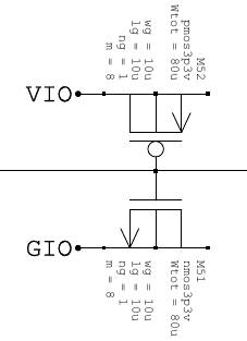
Full circuit is attached, but not that simple sorry. Far above my skill level, real ADC hardware uses a current balancing circuit in between the front end resistors and the modulated capacitor. Here's the capacitor pair. I can make out 10 x 10 = 100 um gate area on each. 3.3 Volt transistor means a thicker dielectric I guess. No idea what Wtot means.
@"Christof Eb." said:
What is the size of these capacitors "C"? As far as I understand, this together with R=450k gives the answer to the question, how long you have to wait after switching the input?
Full circuit is attached, but not that simple sorry. Far above my skill level, real ADC hardware uses a current balancing circuit in between the front end resistors and the modulated capacitor. Here's the capacitor pair. I can make out 10 x 10 = 100 um gate area on each. 3.3 Volt transistor means a thicker dielectric I guess. No idea what Wtot means.
Thank you, evanh!
@cgracey what absolute value in mV do you get, when you connect a pin directly to GND with you new method?
I did some measurements and had the impression, that not noise but the absolute error is the bigger problem?
Yes, the absolute errors at GND and VIO are the biggest problems. I should have designed the ADC differently, so that the same high-z resistor was used for GIO, VIO, and pin measurement. Instead, I have three separate matched resistors that differ more than I thought they would. So, I've seen pins that are as much as 15mV off. The only way to overcome that error is if you are able to drive the pin low (which can be done when using the ADC) and overcome the analog input signal, forcing the pin very close to GND and then measuring it. Same could be done for VIO by driving it high.
To answer the cap question, the 3p3v gate capacitors have a capacitance of 4.4 fF / um2. So, for eight (m=8) 10um x 10um gate caps, that's 3520 fF (4.4 fF * 8 * 10 * 10). Because we have both PMOS and NMOS cap sets for power supply noise rejection, double that to get 7040 fF or about 7 pF. That's not much, but consider that the circuit was designed to run at 200 MHz.
I found a way to make a time-halving, resolution-doubling N-stage filter that takes almost no memory and a constant amount of time to operate. It outputs 17 stages of samples, from the raw base sample to the average of 64K samples.
Here are WHEN the stages are computed for up to stage 7, but the stages could be infinitely higher:
Stage 0 is the ADC sample that is generated each period.
Stage 1 is the sum of two Stage 0 samples. It is generated every second period.
Stage 2 is the sum of two Stage 1 samples. It is generated every fourth period.
Stage 3 is the sum of two Stage 2 samples. It is generated every eighth period.
etc.
I found a way to pick which stage needs to be computed each period by reversing the bits in an incrementing counter, taking the magnitude via ENCOD, then subtracting it from 32.
Each time a stage executes, it outputs a sample by right-shifting its stored value by its stage number.
The idea is that you don't need to specify a sample rate and quality. You just pick the sample stream that gives the best tradeoff between rate and resolution. The ADC is running full speed all the time, generating fast low-res samples.
Here is the code for it, along with the ADC and DAC generator for testing.
This drawing is helpful to understand how it works...
I see it as a current measuring circuit... There is a current coming into to ADC from the voltage applied to the pin, through one of for resistors.
Then, there is current coming from the digital circuit through the 300 kOhm resistor. The digital circuit works to cancel out the input current with it's output current to maintain VIO/2 voltage where they meet.
I think the first of those four buffers in series is more like a voltage comparator than a buffer. Giving 0 if above VIO/2 and 1 if below VIO/2...
So, if one wanted to measure a much higher voltage, could just add an extra series resistor between voltage to be measured and pin.
As long as that resistance was bigger than say, 10k, the protection diodes should keep chip save when ADC is off...
But, probably need to look into spec for how much current protection diodes can take to be sure it's OK...
@Rayman said:
So, if one wanted to measure a much higher voltage, could just add an extra series resistor between voltage to be measured and pin.
Totally, it's a good solution. Maybe throw in a high frequency capacitor from the pin to GIO to absorb spikes.
The ADC electrically centres on VIO/2 so you have to accept that there is an offset. But it's a fixed value voltage and at large voltage ranges the lopsided current becomes insignificant.
Could use the x100 setting for a smaller internal resistor so that the external resistor completely dominates. With internal 5 kOhm, a 50 MOhm to handle up to 500 Volts peak would make any small difference in the coefficients well below noise floor.
PS: That functional drawing was made years before Chip released the full schematic. The 4k5R to 450kR was a pure guess on my part originally. The real x1 resistors are over 500 kOhms.
@evanh said:
Could use the x100 setting for a smaller internal resistor so that the external resistor completely dominates. With internal 5 kOhm, a 50 MOhm to handle up to 500 Volts peak would make any small difference in the coefficients well below noise floor.
PS: That functional drawing was made years before Chip released the full schematic. The 4k5R to 450kR was a pure guess on my part originally. The real x1 resistors are over 500 kOhms.
The pin will bias itself somewhere around VIO/2, but not exactly at VIO/2. So, the amplified modes (ie 100x) need to be allowed to go to their center voltage, because the full range may be as little as 50mV peak-peak around that center voltage. You would want a huge series resistor (megohms) in that case. For AC signals, just a series capacitor is sufficient, since it will allow the DC to settle where it wants, but will convey voltage changes.
Talking about high voltages. I once was given instruction to wipe clean a electronic vacuum valve in a plastic welding machine that was used for manufacturing waterbeds. The DC bus was some thousands of volts. It had a lot of series diodes in the rectifier! The valve wouldn't have fit inside a kitchen oven.
Anyway the circuit breaker had been tripping so my instructions was turn it all off and just carefully use some meths and a rag to clean the whole glass surface of this valve. Ensure it was dry before powering up again.
Voila, it worked a dream. The operators were blasting them sheets of plastic no problem. Gave me the willies to be honest.
@cgracey said:
I found a way to make a time-halving, resolution-doubling N-stage filter that takes almost no memory and a constant amount of time to operate. It outputs 17 stages of samples, from the raw base sample to the average of 64K samples.
The idea is that you don't need to specify a sample rate and quality. You just pick the sample stream that gives the best tradeoff between rate and resolution. The ADC is running full speed all the time, generating fast low-res samples.
If you can dedicate a COG this seems a rather useful way to generate clean/filtered analog results at whatever sample rate you need. I've not messed about with ADCs and DACs on the P2 as yet so having something like this is pretty handy.
With 6 IO pins needed it might be good to build a 2 channel ADC P2 breakout board that leverages this concept. You could put a voltage reference on it for calibration, and you might be able to use the two spare pins in an 8 bit group with an i2c expander to control an analog input mux or FETs to switch in series resistors and capacitors for voltage range extending or AC coupling or to select the voltage reference. Or to keep it simpler, maybe these 2 spare IO pins could just be 2 DAC channel outputs. This could then become a simple 2 channel analog IO P2 breakout with a nominal 0-3.3V voltage range that also has the extra headroom to detect under/over voltage conditions. Might be good to add some bulkier input protection in that case to help protect P2 inputs.
A board like that would be nice.
I started breaking apart the sections of code needed to perform each step of the ADC conversion, in order to make a configurable system that could handle any number of ADCs. When I started putting the state code around it, it got really ugly. Then I had a realization that there was a better way to do it. I could make a bytecode interpreter that could contain all the needed code, kind of like the Spin2 interpreter. Then, rather than put all this stateful code around the core ADC code sections, I could just call them out via bytecodes with very little memory and execution overhead. Plus, configuration becomes super flexible this way.
Here is my current working file on ADC stuff with a bunch of ideas in comments. Martin Montague on the Propeller Live Forum today wanted me to post this. It requires PNut_v43 to run.
@cgracey Is there supposed to be a plot in the scope window? Mine is blank. Just see what looks like text values for the ADCs in the regular debug window....
@Rayman said:
@cgracey Is there supposed to be a plot in the scope window? Mine is blank. Just see what looks like text values for the ADCs in the regular debug window....
Ah, I think it's because you'll need the latest version of PNut and I'm not sure if it's in PropellerTool, yet.
I added an auto-scale function to the SCOPE mode that will confuse older versions of DEBUG.
I've been looking into this code to try to read a current shunt. It looks like with <100uVpp noise that would be 2mA on a 0.05 Ohm shunt. That would be excellent. What is not so good is the 2000-5000 uV offset.
So, I've added an external multiplexer. (Single Pole Double Throw. Maybe SN74LVC1G3157 or equivelent.) The plan was to connect the analog input to 1 of 2 analog pins. Instead of using the ADC Gio/Vio mode, I measure the pin all the time and drive the pin to Gio/Vio by making it an output. I'm only using the readings from 1 pin right now and had about -1000uV of offset.
I measured about 300uV between a ground hole on the Edge module and a ground hole on the breadboard. The current draw was ~80mA. So a resistance of 4 miliOhms could cause that voltage drop. Not that bad. I suppose the bond wires could have a 600uV drop.
We might be able to solve some issues with differential measurement. I've done that to measure +-400V on both P1 and P2 with good accuracy. A 4:1 multiplexer would allow selection of positive and negative references and positive and negative signal values.
It would be nice to not need external parts, but multiplexers are usually pretty cheap when compared to high performance ADCs.
ADC development has gone full circle. Here is the superthread where Chip discovered that tapering the edges of the ADC sampling window significantly improved the quality. https://forums.parallax.com/discussion/169298/adc-sampling-breakthrough/p1 Later, we discovered that a triangular window aka SINC2 would perform even better.
Recently I have been working on a sensorless BLDC motor driver. There is a project showing how to build one of those using Arduino. It uses 3 resistors to simulate a motor ground connection. This voltage is compared to one of the phases to determine commutation. I would rather not need to add the virtual ground resistors to the P2 Universal Motor Driver board. I could use the ADCs to measure the voltages on each pin. The slight problem is the PWM on the motor power. I haven't tested the triangular SINC2 window on a PWM signal yet. But I don't think it would work well. I would expect significant variation depending on the alignment between the PWM signal and the sampling window. I could use P_COUNT_HIGHS to measure the ADC. That should average out the PWM very well if the sample window matches the PWM interval. However, as discovered years ago, sample windows with smooth edges work better.
So I would expect a trapezoid window function to work better than rectangular while also filtering the PWM away. How to generate such a thing efficiently? Summing together overlapping SINC2 samples would work. (This is what I think Chip's code in this thread does.) That creates a trade-off. I want a relatively short ramp up and down on the sides so I can measure the average voltage of a PWM signal. But that would require a higher sampling rate and a lot of clock cycles to add all those samples together at the top of the trapezoid. Not ideal. Based on my simulations and intuition, I think that the samples in the middle of the trapezoid cancel each other out of the calculations. So it is only necessary to acquire 2 samples at the beginning and 2 at the end.
One last hurdle. The P2 smart pin does one of the differentiations in hardware. Normally that is great because it saves 2 instructions and some memory. To make the trapezoidal sampling work, I needed a continuous double integration of the ADC bitstream. I set it to a 1 clock sampling interval to get the pin to update every clock. Then the pin must be set to SINC3 mode. The first integrator is continually reset, so the data is double integrated.
There are a few neat things that can be done with this new technique.
1. Multiple cogs can read the same ADC, even at different sample rates and without any concern about sample overlap.
2. The sampling window can start and stop at any time. The multiplexer settling time, window ramp up, and window top are all independent now.
3. By taking many more samples during the ramp up and ramp down phases we can create a big Tukey window.
The proof of concept code attached seems to perform similarly to Chip's code when using 1 pin. The only metric I looked at as peak to peak noise.
@SaucySoliton said:
... It uses 3 resistors to simulate a motor ground connection. This voltage is compared to one of the phases to determine commutation. I would rather not need to add the virtual ground resistors to the P2 Universal Motor Driver board. I could use the ADCs to measure the voltages on each pin. The slight problem is the PWM on the motor power.
I don't really understand what you are actually measuring. If you have 3 PWM outputs at the motor terminals then the voltage at the virtual star point could be calculated and there is no need to measure anything. The star point voltage should be very close to the average of the PWM duty cycles multiplied with the DC bus voltage. There are only tiny variations due to the voltage drop of current times Rdson resistance but as the sum of all currents is zero they should also nearly cancel out.
So I guess you only have two active PWM outputs and let the third motor terminal float. Then it makes sense to compare the voltage of that floating motor phase to the virtual star point.
@ManAtWork said:
So I guess you only have two active PWM outputs and let the third motor terminal float. Then it makes sense to compare the voltage of that floating motor phase to the virtual star point.
Exactly. The floating leg is used to detect the rotor position. Although I will only have 1 leg with PWM and the other active leg will be grounded. I'm hoping it will be a little more efficient that way.
@ErNa said:
What is the speed range you want to run the motor sensorlessly?
A bit slower than the minimum speed on those Gemfan ESCs that Parallax used to carry. The motor can actually turn very slow when fed 3 phase PWM. The rotation isn't that smooth but it works. That leaves a middle speed range that is too fast to self start and too slow for the ESC to run. As seen in the Arduino project I linked above, a sensorless ESC doesn't have to be complicated. It would be that simple on the P2 if the ADC did not need calibration.
@evanh said:
Constant torque at zero speed, one hopes.
Probably need a sensored motor for that. Maybe it could be done with precise motor current measurements. The current measurement on the RevA Universal Motor Driver isn't that accurate because it's missing the current sense amplifier like RevB has. I'm thinking the purpose of the last mystery box was to move out those RevA boards.
Since a picture is worth 1000 words,
The blue line is partly hidden by the purple line. The blue, yellow, and red lines are a 3 phase signal, shifted so that the minimum value is always 0. And normalized so the maximum is always 1. The purple line is validation that the top arches can be calculated with only a single sin() operation.
The top arches are always sine from pi/3 to 2pi/3. The rising/falling lines are sine from 0 to pi/3, sometimes mirrored. So I can generate a 3 phase signal while only doing 2 QROTATEs. An additional benefit is the bottom line does not need PWM, so it should be a tiny bit more efficient.
With the resources of the P2, we aren't limited to a simple comparison of the rising/falling voltages. Maybe I could do something like fit a line to the ADC measurements and compare that to the expected line.
@Electrodude said:
Isn't it faster to just do three interleaved qrotates on θ, θ+π/3, and θ+2π/3 than to have to bother with handling each of the sextants specially?
Maybe not. After the 3 qrotates I would need to find the minimum and maximum. Then subtract all by the minimum. The phase that is neither maximum nor minimum should be left floating. In the process of subtracting 2 3-phase sine terms, a scale factor of sqrt(3) is introduced.
But I read that some BLDC motors are designed for trapezoidal current. https://www.ti.com/lit/ml/slyp711/slyp711.pdf The way I structured the code, I can get the trapezoidal waveform by simply skipping the qrotate. The third phase with intermediate voltage isn't driven under such a scheme.
@SaucySoliton said:
But I read that some BLDC motors are designed for trapezoidal current.
In industrial servo motor land, I had the impression that's the difference between BLAC and BLDC. The other difference is BLAC always uses a resolver for feedback. The hall sensors + encoder don't exist then. Encoder is emulated in the drive as a freebie output to any subsequent motion controller. I never saw one but early forms, pre-1990's, were all analogue too.
I never learnt what is structurally different between them though.
PS: Apparently, the correct term for BLAC is Permanent Magnet Synchronous Machines (PMSM).
A DC motor is a DC motor, an AC motor is an AC motor. That is the difference. A motor creates torque from current. A BLDC motor creates constant torque from constant "DC-current" when the rotor sweeps 60°. So the motor is designed to keep the torque constant over 60°. DC has no phase angle. There is just one closed loop running one current. If you switch the loop from phase to phase, that doesn't make DC an AC.
In this sense, common single phase "AC" is just DC with changing amplitude and even sign.
"True" AC is a three phase current. There no longer is one loop to carry the current, but there are three wires and two current pathes. That gives AC another parameter besides amplitude: the phase angle.
An AC motor is not designed to create constant torque if two terminals are driven with DC. Torque now changes with the rotor angle in a sinoidal way. But if you drive an AC motor with an AC current and the phase angle of the current is aligned with the position of the rotor, then the torque generated is proportional to the current amplitude and not depending on the rotor angle.
The voltage side looks like this:
You just can not apply a voltage to a motor. Whenever you switch on the voltage to the terminals, you apply the voltage to the inductance of the motor and the resistance of the winding. But as the motor runs, the motor generates a voltage, called Back Voltage, or Back Electro Motoric Force. EMF is just an outdated word for voltage. It is reasoned in the fact, that the force coming out of a galvanic cell could generate the motion of frog legs. So "motoric" is just linked to motion, not to a motor, which at that time didn't exist.
As the motor generates a voltage when running which now has to be overwhelmed by the current, electrical power is converted to mechanical power.
A DC motor generates a constant DC voltage, there is nothing "trapezoidal". What can be measured at the floating pin is NOT the BEMF, but the BEMF multiplied by the phase angle of the rotor (30° to -30°). So what you measure is actually the rotor angle.
An AC motor on the other hand generates AC voltage, that is, a three phase voltage of given amplitude and phase angle. Again, the amplitude is proportional to the rotational speed and so take care of power transmission.
But to "rotate" the current in presence of the inductance of the motor it takes some voltage that is phase shifted by 90° to the current. For this reason the voltages applied to drive the motor (power) and to commutate the current add up to form a AC Voltage, that is a little phase shifted to the current. To keep this phase shift in the correct state, the FOC is mostly used.
There is a distinct DC motor and a distinct AC motor. But real motors always differ from the ideal, more or less by accident or intentionally. And that give plenty of room for rumor.


Comments
Full circuit is attached, but not that simple sorry. Far above my skill level, real ADC hardware uses a current balancing circuit in between the front end resistors and the modulated capacitor. Here's the capacitor pair. I can make out 10 x 10 = 100 um gate area on each. 3.3 Volt transistor means a thicker dielectric I guess. No idea what Wtot means.
Thank you, evanh!
@cgracey what absolute value in mV do you get, when you connect a pin directly to GND with you new method?
I did some measurements and had the impression, that not noise but the absolute error is the bigger problem?
Yes, the absolute errors at GND and VIO are the biggest problems. I should have designed the ADC differently, so that the same high-z resistor was used for GIO, VIO, and pin measurement. Instead, I have three separate matched resistors that differ more than I thought they would. So, I've seen pins that are as much as 15mV off. The only way to overcome that error is if you are able to drive the pin low (which can be done when using the ADC) and overcome the analog input signal, forcing the pin very close to GND and then measuring it. Same could be done for VIO by driving it high.
To answer the cap question, the 3p3v gate capacitors have a capacitance of 4.4 fF / um2. So, for eight (m=8) 10um x 10um gate caps, that's 3520 fF (4.4 fF * 8 * 10 * 10). Because we have both PMOS and NMOS cap sets for power supply noise rejection, double that to get 7040 fF or about 7 pF. That's not much, but consider that the circuit was designed to run at 200 MHz.
I found a way to make a time-halving, resolution-doubling N-stage filter that takes almost no memory and a constant amount of time to operate. It outputs 17 stages of samples, from the raw base sample to the average of 64K samples.
Here are WHEN the stages are computed for up to stage 7, but the stages could be infinitely higher:
00000000000000000000000000000000000000000000000000000000000000000
 1 1 1 1 1 1 1 1 1 1 1 1 1 1 1 1 1 1 1 1 1 1 1 1 1 1 1 1 1 1 1 1
  2   2   2   2   2   2   2   2   2   2   2   2   2   2   2   2
    3       3       3       3       3       3       3       3
        4               4               4               4
                5                               5
                                6
                                                                7
Stage 0 is the ADC sample that is generated each period.
Stage 1 is the sum of two Stage 0 samples. It is generated every second period.
Stage 2 is the sum of two Stage 1 samples. It is generated every fourth period.
Stage 3 is the sum of two Stage 2 samples. It is generated every eighth period.
etc.
I found a way to pick which stage needs to be computed each period by reversing the bits in an incrementing counter, taking the magnitude via ENCOD, then subtracting it from 32.
Each time a stage executes, it outputs a sample by right-shifting its stored value by its stage number.
The idea is that you don't need to specify a sample rate and quality. You just pick the sample stream that gives the best tradeoff between rate and resolution. The ADC is running full speed all the time, generating fast low-res samples.
Here is the code for it, along with the ADC and DAC generator for testing.
This drawing is helpful to understand how it works...
I see it as a current measuring circuit... There is a current coming into to ADC from the voltage applied to the pin, through one of for resistors.
Then, there is current coming from the digital circuit through the 300 kOhm resistor. The digital circuit works to cancel out the input current with it's output current to maintain VIO/2 voltage where they meet.
I think the first of those four buffers in series is more like a voltage comparator than a buffer. Giving 0 if above VIO/2 and 1 if below VIO/2...
So, if one wanted to measure a much higher voltage, could just add an extra series resistor between voltage to be measured and pin.
As long as that resistance was bigger than say, 10k, the protection diodes should keep chip save when ADC is off...
But, probably need to look into spec for how much current protection diodes can take to be sure it's OK...
Totally, it's a good solution. Maybe throw in a high frequency capacitor from the pin to GIO to absorb spikes.
The ADC electrically centres on VIO/2 so you have to accept that there is an offset. But it's a fixed value voltage and at large voltage ranges the lopsided current becomes insignificant.
On paper, yes.
In practice the on chip resistors have a tempco that should be matched by that external R.
Could use the x100 setting for a smaller internal resistor so that the external resistor completely dominates. With internal 5 kOhm, a 50 MOhm to handle up to 500 Volts peak would make any small difference in the coefficients well below noise floor.
PS: That functional drawing was made years before Chip released the full schematic. The 4k5R to 450kR was a pure guess on my part originally. The real x1 resistors are over 500 kOhms.
The pin will bias itself somewhere around VIO/2, but not exactly at VIO/2. So, the amplified modes (ie 100x) need to be allowed to go to their center voltage, because the full range may be as little as 50mV peak-peak around that center voltage. You would want a huge series resistor (megohms) in that case. For AC signals, just a series capacitor is sufficient, since it will allow the DC to settle where it wants, but will convey voltage changes.
Oops, you reminded me, 50 MOhm makes 500 V peak-peak, so only 250 V peak.
Talking about high voltages. I once was given instruction to wipe clean a electronic vacuum valve in a plastic welding machine that was used for manufacturing waterbeds. The DC bus was some thousands of volts. It had a lot of series diodes in the rectifier! The valve wouldn't have fit inside a kitchen oven.
Anyway the circuit breaker had been tripping so my instructions was turn it all off and just carefully use some meths and a rag to clean the whole glass surface of this valve. Ensure it was dry before powering up again.
Voila, it worked a dream. The operators were blasting them sheets of plastic no problem. Gave me the willies to be honest.
If you can dedicate a COG this seems a rather useful way to generate clean/filtered analog results at whatever sample rate you need. I've not messed about with ADCs and DACs on the P2 as yet so having something like this is pretty handy.
With 6 IO pins needed it might be good to build a 2 channel ADC P2 breakout board that leverages this concept. You could put a voltage reference on it for calibration, and you might be able to use the two spare pins in an 8 bit group with an i2c expander to control an analog input mux or FETs to switch in series resistors and capacitors for voltage range extending or AC coupling or to select the voltage reference. Or to keep it simpler, maybe these 2 spare IO pins could just be 2 DAC channel outputs. This could then become a simple 2 channel analog IO P2 breakout with a nominal 0-3.3V voltage range that also has the extra headroom to detect under/over voltage conditions. Might be good to add some bulkier input protection in that case to help protect P2 inputs.
A board like that would be nice.
I started breaking apart the sections of code needed to perform each step of the ADC conversion, in order to make a configurable system that could handle any number of ADCs. When I started putting the state code around it, it got really ugly. Then I had a realization that there was a better way to do it. I could make a bytecode interpreter that could contain all the needed code, kind of like the Spin2 interpreter. Then, rather than put all this stateful code around the core ADC code sections, I could just call them out via bytecodes with very little memory and execution overhead. Plus, configuration becomes super flexible this way.
Sounds like doing it with Forth....
Here is my current working file on ADC stuff with a bunch of ideas in comments. Martin Montague on the Propeller Live Forum today wanted me to post this. It requires PNut_v43 to run.
@cgracey
chip,
Can the single Pin version be modified to run two adc channels at the same time or should it be run in two cogs?
Jim
Eight ADC pins at once with bytecode interpreter.
@cgracey Is there supposed to be a plot in the scope window? Mine is blank. Just see what looks like text values for the ADCs in the regular debug window....
Ah, I think it's because you'll need the latest version of PNut and I'm not sure if it's in PropellerTool, yet.
I added an auto-scale function to the SCOPE mode that will confuse older versions of DEBUG.
I've been looking into this code to try to read a current shunt. It looks like with <100uVpp noise that would be 2mA on a 0.05 Ohm shunt. That would be excellent. What is not so good is the 2000-5000 uV offset.
So, I've added an external multiplexer. (Single Pole Double Throw. Maybe SN74LVC1G3157 or equivelent.) The plan was to connect the analog input to 1 of 2 analog pins. Instead of using the ADC Gio/Vio mode, I measure the pin all the time and drive the pin to Gio/Vio by making it an output. I'm only using the readings from 1 pin right now and had about -1000uV of offset.
I measured about 300uV between a ground hole on the Edge module and a ground hole on the breadboard. The current draw was ~80mA. So a resistance of 4 miliOhms could cause that voltage drop. Not that bad. I suppose the bond wires could have a 600uV drop.
We might be able to solve some issues with differential measurement. I've done that to measure +-400V on both P1 and P2 with good accuracy. A 4:1 multiplexer would allow selection of positive and negative references and positive and negative signal values.
It would be nice to not need external parts, but multiplexers are usually pretty cheap when compared to high performance ADCs.
ADC development has gone full circle. Here is the superthread where Chip discovered that tapering the edges of the ADC sampling window significantly improved the quality. https://forums.parallax.com/discussion/169298/adc-sampling-breakthrough/p1 Later, we discovered that a triangular window aka SINC2 would perform even better.
Recently I have been working on a sensorless BLDC motor driver. There is a project showing how to build one of those using Arduino. It uses 3 resistors to simulate a motor ground connection. This voltage is compared to one of the phases to determine commutation. I would rather not need to add the virtual ground resistors to the P2 Universal Motor Driver board. I could use the ADCs to measure the voltages on each pin. The slight problem is the PWM on the motor power. I haven't tested the triangular SINC2 window on a PWM signal yet. But I don't think it would work well. I would expect significant variation depending on the alignment between the PWM signal and the sampling window. I could use P_COUNT_HIGHS to measure the ADC. That should average out the PWM very well if the sample window matches the PWM interval. However, as discovered years ago, sample windows with smooth edges work better.
So I would expect a trapezoid window function to work better than rectangular while also filtering the PWM away. How to generate such a thing efficiently? Summing together overlapping SINC2 samples would work. (This is what I think Chip's code in this thread does.) That creates a trade-off. I want a relatively short ramp up and down on the sides so I can measure the average voltage of a PWM signal. But that would require a higher sampling rate and a lot of clock cycles to add all those samples together at the top of the trapezoid. Not ideal. Based on my simulations and intuition, I think that the samples in the middle of the trapezoid cancel each other out of the calculations. So it is only necessary to acquire 2 samples at the beginning and 2 at the end.
One last hurdle. The P2 smart pin does one of the differentiations in hardware. Normally that is great because it saves 2 instructions and some memory. To make the trapezoidal sampling work, I needed a continuous double integration of the ADC bitstream. I set it to a 1 clock sampling interval to get the pin to update every clock. Then the pin must be set to SINC3 mode. The first integrator is continually reset, so the data is double integrated.
There are a few neat things that can be done with this new technique.
1. Multiple cogs can read the same ADC, even at different sample rates and without any concern about sample overlap.
2. The sampling window can start and stop at any time. The multiplexer settling time, window ramp up, and window top are all independent now.
3. By taking many more samples during the ramp up and ramp down phases we can create a big Tukey window.
The proof of concept code attached seems to perform similarly to Chip's code when using 1 pin. The only metric I looked at as peak to peak noise.
I don't really understand what you are actually measuring. If you have 3 PWM outputs at the motor terminals then the voltage at the virtual star point could be calculated and there is no need to measure anything. The star point voltage should be very close to the average of the PWM duty cycles multiplied with the DC bus voltage. There are only tiny variations due to the voltage drop of current times Rdson resistance but as the sum of all currents is zero they should also nearly cancel out.
So I guess you only have two active PWM outputs and let the third motor terminal float. Then it makes sense to compare the voltage of that floating motor phase to the virtual star point.
Exactly. The floating leg is used to detect the rotor position. Although I will only have 1 leg with PWM and the other active leg will be grounded. I'm hoping it will be a little more efficient that way.
I'm following this design: https://simple-circuit.com/arduino-sensorless-bldc-motor-controller-esc/
What is the speed range you want to run the motor sensorlessly?
Constant torque at zero speed, one hopes.
A bit slower than the minimum speed on those Gemfan ESCs that Parallax used to carry. The motor can actually turn very slow when fed 3 phase PWM. The rotation isn't that smooth but it works. That leaves a middle speed range that is too fast to self start and too slow for the ESC to run. As seen in the Arduino project I linked above, a sensorless ESC doesn't have to be complicated. It would be that simple on the P2 if the ADC did not need calibration.
Probably need a sensored motor for that. Maybe it could be done with precise motor current measurements. The current measurement on the RevA Universal Motor Driver isn't that accurate because it's missing the current sense amplifier like RevB has. I'm thinking the purpose of the last mystery box was to move out those RevA boards.
Since a picture is worth 1000 words,
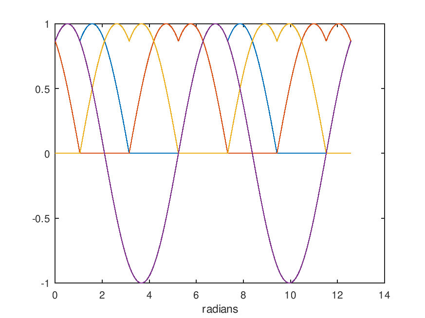
The blue line is partly hidden by the purple line. The blue, yellow, and red lines are a 3 phase signal, shifted so that the minimum value is always 0. And normalized so the maximum is always 1. The purple line is validation that the top arches can be calculated with only a single sin() operation.
The top arches are always sine from pi/3 to 2pi/3. The rising/falling lines are sine from 0 to pi/3, sometimes mirrored. So I can generate a 3 phase signal while only doing 2 QROTATEs. An additional benefit is the bottom line does not need PWM, so it should be a tiny bit more efficient.
With the resources of the P2, we aren't limited to a simple comparison of the rising/falling voltages. Maybe I could do something like fit a line to the ADC measurements and compare that to the expected line.
Isn't it faster to just do three interleaved
qrotates onθ,θ+π/3, andθ+2π/3than to have to bother with handling each of the sextants specially?Maybe not. After the 3
qrotates I would need to find the minimum and maximum. Then subtract all by the minimum. The phase that is neither maximum nor minimum should be left floating. In the process of subtracting 2 3-phase sine terms, a scale factor ofsqrt(3)is introduced.But I read that some BLDC motors are designed for trapezoidal current. https://www.ti.com/lit/ml/slyp711/slyp711.pdf The way I structured the code, I can get the trapezoidal waveform by simply skipping the qrotate. The third phase with intermediate voltage isn't driven under such a scheme.
In industrial servo motor land, I had the impression that's the difference between BLAC and BLDC. The other difference is BLAC always uses a resolver for feedback. The hall sensors + encoder don't exist then. Encoder is emulated in the drive as a freebie output to any subsequent motion controller. I never saw one but early forms, pre-1990's, were all analogue too.
I never learnt what is structurally different between them though.
PS: Apparently, the correct term for BLAC is Permanent Magnet Synchronous Machines (PMSM).
A DC motor is a DC motor, an AC motor is an AC motor. That is the difference. A motor creates torque from current. A BLDC motor creates constant torque from constant "DC-current" when the rotor sweeps 60°. So the motor is designed to keep the torque constant over 60°. DC has no phase angle. There is just one closed loop running one current. If you switch the loop from phase to phase, that doesn't make DC an AC.
In this sense, common single phase "AC" is just DC with changing amplitude and even sign.
"True" AC is a three phase current. There no longer is one loop to carry the current, but there are three wires and two current pathes. That gives AC another parameter besides amplitude: the phase angle.
An AC motor is not designed to create constant torque if two terminals are driven with DC. Torque now changes with the rotor angle in a sinoidal way. But if you drive an AC motor with an AC current and the phase angle of the current is aligned with the position of the rotor, then the torque generated is proportional to the current amplitude and not depending on the rotor angle.
The voltage side looks like this:
You just can not apply a voltage to a motor. Whenever you switch on the voltage to the terminals, you apply the voltage to the inductance of the motor and the resistance of the winding. But as the motor runs, the motor generates a voltage, called Back Voltage, or Back Electro Motoric Force. EMF is just an outdated word for voltage. It is reasoned in the fact, that the force coming out of a galvanic cell could generate the motion of frog legs. So "motoric" is just linked to motion, not to a motor, which at that time didn't exist.
As the motor generates a voltage when running which now has to be overwhelmed by the current, electrical power is converted to mechanical power.
A DC motor generates a constant DC voltage, there is nothing "trapezoidal". What can be measured at the floating pin is NOT the BEMF, but the BEMF multiplied by the phase angle of the rotor (30° to -30°). So what you measure is actually the rotor angle.
An AC motor on the other hand generates AC voltage, that is, a three phase voltage of given amplitude and phase angle. Again, the amplitude is proportional to the rotational speed and so take care of power transmission.
But to "rotate" the current in presence of the inductance of the motor it takes some voltage that is phase shifted by 90° to the current. For this reason the voltages applied to drive the motor (power) and to commutate the current add up to form a AC Voltage, that is a little phase shifted to the current. To keep this phase shift in the correct state, the FOC is mostly used.
There is a distinct DC motor and a distinct AC motor. But real motors always differ from the ideal, more or less by accident or intentionally. And that give plenty of room for rumor.