

Heat sink on mosfets: methods
 T Chap
Posts: 4,260
T Chap
Posts: 4,260
Hello all. I have a P1 based system that drives brushless DC motors. On the typical system the motor runs under low stress and runs for 10 seconds and is off most of the time. I have a case that is high loads and the motor can get stalled and a mosfet can melt the solder. These are 30amp IRF540 type n channel mosfets. 3 are high side 24VDC and 3 are low side. The load is so high that trying to set a current trip threshold above some limit monitored by the P1 via ADS1115 16bit A2D chip doesn’t allow a good headroom to kill the motor because the stress is dynamic and not fixed. What I want to do as a bandaide is add heat sinks. These PCBs have very little copper on top and bottom of the SMT mosfet pads. For a fast PCB update I’m thinking to convert to TH mosfets and add one solid aluminum plane to the high side - as all large pads are 24V on the high. The 3 low side large pads must be separate. What is the most idea what sink in smallest form factor I can stick on the back of vertical mounted mosfets? Thanks.
Comments
This is the board.
How are you driving the gates? I helped design a DMX fixture controller with a big MOSFET and we could not use a heatsink due to space constraints. Around the time Phil Pilgrim had mentioned the TC4427 MOSFET gate driver and it has become one of my favorite components with Propeller circuits. We used the TC4427 to drive the gate of the MOSFET to very near its limit; this reduced wattage across the MOSFET and the circuit worked (24V lamp fixture running 5A through the circuit) -- the client even won a design award for the end product.
I'm a simple guy, so I get it if you're shaking your head saying, "Yeah, JonnyMac, we already took care of that."
The P1 drives a BLDC controller chip MC33035 that drives a BLDC Mosfet Driver IC HP4086. But I have almost no heat sinking and in 30 seconds at 10 Amps these mosfets can get hot. When the motor stalls I do try to kill the motor after Var StallTimer senses no encoder movement when there should be motion. Also checking current on the ADC for an over current trip. But still…. Need some heat solution I think.
One question is what is the best material for a heat sink. I can machine aluminum most easiest. I was thinking 1/8” with some fins. Heat sink grease. Or is thinner material better.
Using a different MOSFET with a lower Rds ON value will reduce much of the heat generated from the MOSFETS.
The IRF540 you are using has an Rds On value of 44 milli Ohms
The TK7R7P10PL,RQ has an Rds On value of 6.5 milli Ohms
Note:
With an Rds of 44m ... at 30 Amps the MOSFET will need to dissipate 39.6 Watts with 1.32V across the SD junction
With an Rds of 6.5m ... at 30 Amps the MOSFET will need to dissipate 5.85 Watts with 195mV across the SD junction
Another thing if you have the real-estate and can spin a new board, you can incorporate a Heat Sink into the PCB itself
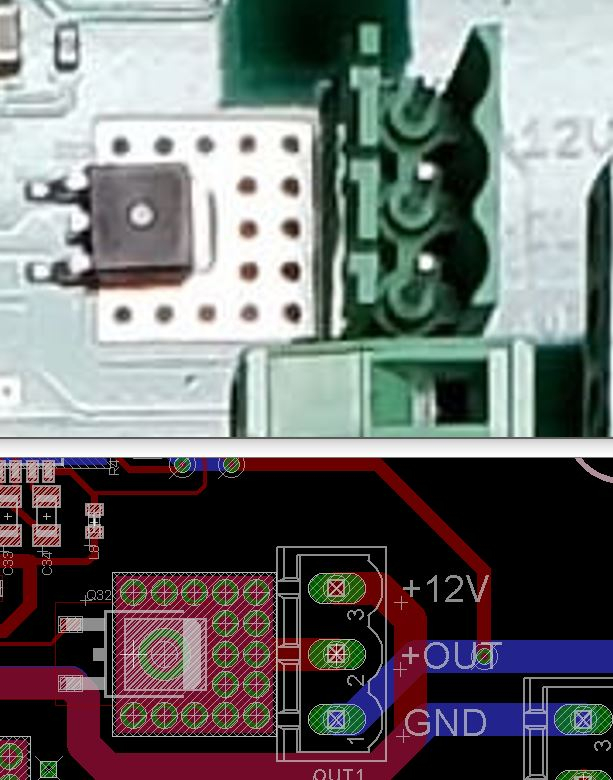
I have 12 boards to upgrade, the backplanes don't allow me to grow the boards, only up.
I used IRF540 as a generic term, these is more real that is probably on the boards now. Rds is like what you are showing.
https://www.infineon.com/dgdl/irf3710zpbf.pdf?fileId=5546d462533600a4015355dfb3991950
I think if I just use a TH version and put some storebought heat sinks on it it will be far better than what I have which is just the solder pad area top and bottom of the large pad.
With those transistors,
At 30 Amps, that's still 16.2 Watts with 540mV across the SD Junction.
With the right transistor you could reduce the MOSFET heat by almost a factor of 3
T Chap,
You can buy finned Aluminum extrusions and be sure to anodize them when you done cutting them.
Beau. I looked at the TK7R7P10PL,RQ, I use DPAK2. I don't see a TH variant of that part but will start searching for a low Rds type TH and see what I can find.
Wow, that's some thermal cutout feature !
As mentioned, you should lower the RDS - you can buy MOSFETSs as low as 0.3m Ohms these days.
DPAK2 is somewhat old, so the newest parts do not use that 3-pin package.
Digikey shows
TKR74F04PB,LXGQ MOSFET N-CH 40V 250A 0.74mOhm @ 125A, 10V with a larger source pin, but tagged not for new designs.
and there is
AUIRFS8408-7TRL MOSFET N-CH 40V 240A D2PAK 10V 1mOhm @ 100A, 10V
for a board revision, lcsc show
HYG006N04LS1TA HUAYI 40V 600A 428W 0.45mΩ@10V,80A in a ~12mm x 10mm SMD package
and small packages
TPHR9003NL,L1Q TOSHIBA 30V 60A 1.6W 0.9mΩ@10V,30A N Channel DSOP-8-EP-5.0mm in ~ 5mm x 6mm package
You can also put multiple thermal vias under the pad, to get heat to the other side faster.
There are solder-on heatsinks, but they are somewhat wimpy, and lower RDS fets make them less necessary.
Thanks for the part numbers! TPHR9003NL,L1Q there are plenty at DigiKey. I dont know if I have the space on top and bottom to put enough copper for proper sink even with a nice array of vias. But it’s a good option. I’d like to find an alternative in 220 package and use off the shelf sinks, maybe a low Rds exists in 220 I’ll search.
PSMN1R1-30PL,127
1.3m Rds
Seems digi has a number of low Rds to220 parts. Maybe a simple fix to make a PCB and add the biggest sinks screwed to it
I keep 0.25”x1.25” aluminum bar stock on hand, and a chuck of that set firmly behind each vertical triplet of mosfets would have sufficient heat capacity to slow down the thermal response a lot, compared with the pcb copper layer. I agree about finding lower Rds mosfets.
Thanks Tracy. I was thinking to CNC an aluminum bar with slots/fins cut in to attach to all 3 of the high side TH mosfets. Then possibly a single piece also on the low side separating each with a mica washer. 1/4” material with some slots cut in for more surface area. Alternatively 3 separate sections on the low side without mica washers. So one big solid piece on low side separated with mica vs 3 separate pieces direct mosfet to aluminum. All with thermal grease. I don’t know how to know which is best
I believe solid piece for all three would be more stable, mechanically, thus mica+grease or sil-pad insulators on the low side. It takes a while to heat up the thermal inertia of a thick Al bar, or angle or channel extrusion. Can the ADC be reconfigured to set a trip point based on temperature of the heat sink or transistor? Is a fan possible?
I started converting the SMT mosfet board to TH. Keeping all the other SMT parts in the same place so as to use the existing stainless stencil. The ADC is ADS1115 so I have I2C already on the board. I use MAX6634 temperature IC’s on projects which are addressable. I could put them on a little breakout board, attach the little boards to the aluminum heat sinks for high and low side. Read the temp every 25-50 ADC reads. Shut down at X temp. Who knows how much noise would get on the wires running to these little breakout boards. Seems iffy. There have been several failures where a mosfet melts solder and slides. I believe this is due to a stall or heavy load causing heat to short the mosfets. The ADC trip threshold should catch the overload but it’s not that simple to do. I think a shorted mosfet is doing the solder melting. I really don’t have any heat sinking on these boards. So the TH part with aluminum plus low Rds should make a difference. It’s good to have gotten some great input on this.
The ADC is ADS1115. 4 channel single ended inputs. I am only using 1 input. I can just add to 2 Inputs. High and low temp measured off the 2 aluminum sinks. The question would still be having wires ran to the sensor mounted on the aluminum picking up lots of noise.
Differential inputs to the ads1115 can ameliorate the noise issue. Use channel 3 as the common reference input, and two other channels as the signal inputs. For best results, run the signal and reference wires as a shielded pair.
To clarify, the ads1115 can do pure differential paired on 0:1 and on channels 2:3, and it can do triple pseudo- differential with a single reference point on 3:2, 3:1 and 3:0. Here is how I set it up for 3 thermocouples, with an IC temperature sensor providing the both the cold junction reference and the common reference on channel 3. If you were to use two LM61s as your temperature sensors, ad3 would be connected to ground on both of them in a way that rejects pcb ground currents and shielding to reject induced noise.
uV1 := adc0.readExplicit(adc0#DIFFERENTIAL_32, adc0#PGA_16)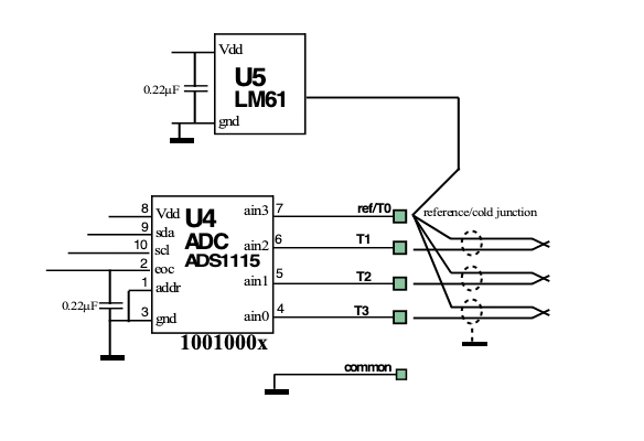
uV2 := adc0.readExplicit(adc0#DIFFERENTIAL_31, adc0#PGA_16)
uV3 := adc0.readExplicit(adc0#DIFFERENTIAL_30, adc0#PGA_16)![]
Thanks Tracy, that's interesting. I never thought of doing that trick.This is what I have now that works well and I haven't noticed any noise creating problems even under loads.
Input AIN0 is from an OpAmp off of the INA138. Single ended. The other 3 inputs are held low with 10k and 4.7uF. They are connected to test pads so they can be used if needed. I added a connectors to run 5V/GND/signal to the 2 temp sensors LM61. Shielded is easy, it's actual just 2" runs. I could do what you are suggesting with Ref on AIN3, 2 sensors on AIN1 and AIN2. It's been a while since I read the ADC datasheet so I need to study which modes to set this to. I don't recall a method to set one input as reference but I'll look at it again.
"ad3 would be connected to ground on both of them"
Meaning connected to ground plane? Or connect to GND of the sensor AT the sensors. 2 wires from AIN3 run to the sensors GND pin? Not sure what you meant.
I think I see what you are doing. It requires setting the config registers before each read. This allows you to use ain3 as the negative input for positive inputs 0/1/2.
The temp reads could be at a much lower read rate versus the current sense. Maybe read temp every 100 current reads.
While I’m thinking on this concept I wonder if there is a way to include ain0 from the current sense as part of the pseudo differential multiplex scheme with the 2 temp sensors.
With the LM61 on short cables, I think I'd simply hook them up and read them single ended, same as your INA138. Just keep all the grounds bundled together near Vss on the ADS1115. At 10mV/°C, their output is far less subject to noise than the µV levels from thermocouples.
degC * 10 = mV - 600
-30 degC is 300mV
0 degC is 600mV
60 degC is 1200mV
Thanks for the suggestions! I set it up so ain3 can be ground with 1 and 2 as temp sensors. Then I can test the differential concept on any or all inputs 1/2/3
Wish you'd post more often...always sure of a good read")
Craig
Need to machine the aluminum heat sinks and see if the smoke comes out.
The first issue is, the motor runs normally( test motor no load). But all 3 high side transistors are equally baking hot within 10 seconds(cannot touch) even under no load. Low sides are not hot. Disconnect BLDC motor, apply same input (speed control voltage) and no heat on high sides. The 3 high side n channel mosfets have 26VDC on the drain(tabs) . The 3 low sides have the source to GND via .1 ohm sense resistor 3 watt.
I just realized I bought a low Rds TO220 that is Logic Level. 30V, I am provided around 27V. The mosfet driver I use is a HIP4086. a 3 high, 3 low N channel mosfet driver with built-in charge pumps. I see 40V peaks on the high side gate inputs. gate-source voltage +/-20V. But this is the same Gate-Source rating as all other non logic level versions.
https://assets.nexperia.com/documents/data-sheet/PSMN1R1-30PL.pdf
https://renesas.com/us/en/products/power-power-management/fet-motor-drivers/3-phase-mosfet-drivers-3-phase-fet-drivers/hip4086-80v-500ma-3-phase-mosfet-driver?gclid=CjwKCAiA6byqBhAWEiwAnGCA4MApPMopK4W5jXYvghfoRHxn2sId5pJFxdTsiUnhYv6lmqvBZGrR8RoCd_wQAvD_BwE#overview
As a test I rigged up one of my go to SMT n channel non logic level mosfets on just one of the high sides and there is no discernible heat on that one while the other 2 are baking.
I replaced the new TO220 mosfets with some SMT version and have no discernible heat.
The BLDC driver IC has a built in current limited circuit using a .1 sensor resistor on the low side to GND. The fault light was showing a lot of "stress" before changing out the high side mosfets. Now it all seems normal.
Since all 3 high side mosfets were hot, I can only assume that the logic level inputs on the high side didnt like the 40V peak. The low side mosfets only get 20V from the mosfet driver. When driving all n channel mosfets, the high side must be driven with significantly higher voltages.