

Spinner Edge board
 ke4pjw
Posts: 1,188
ke4pjw
Posts: 1,188
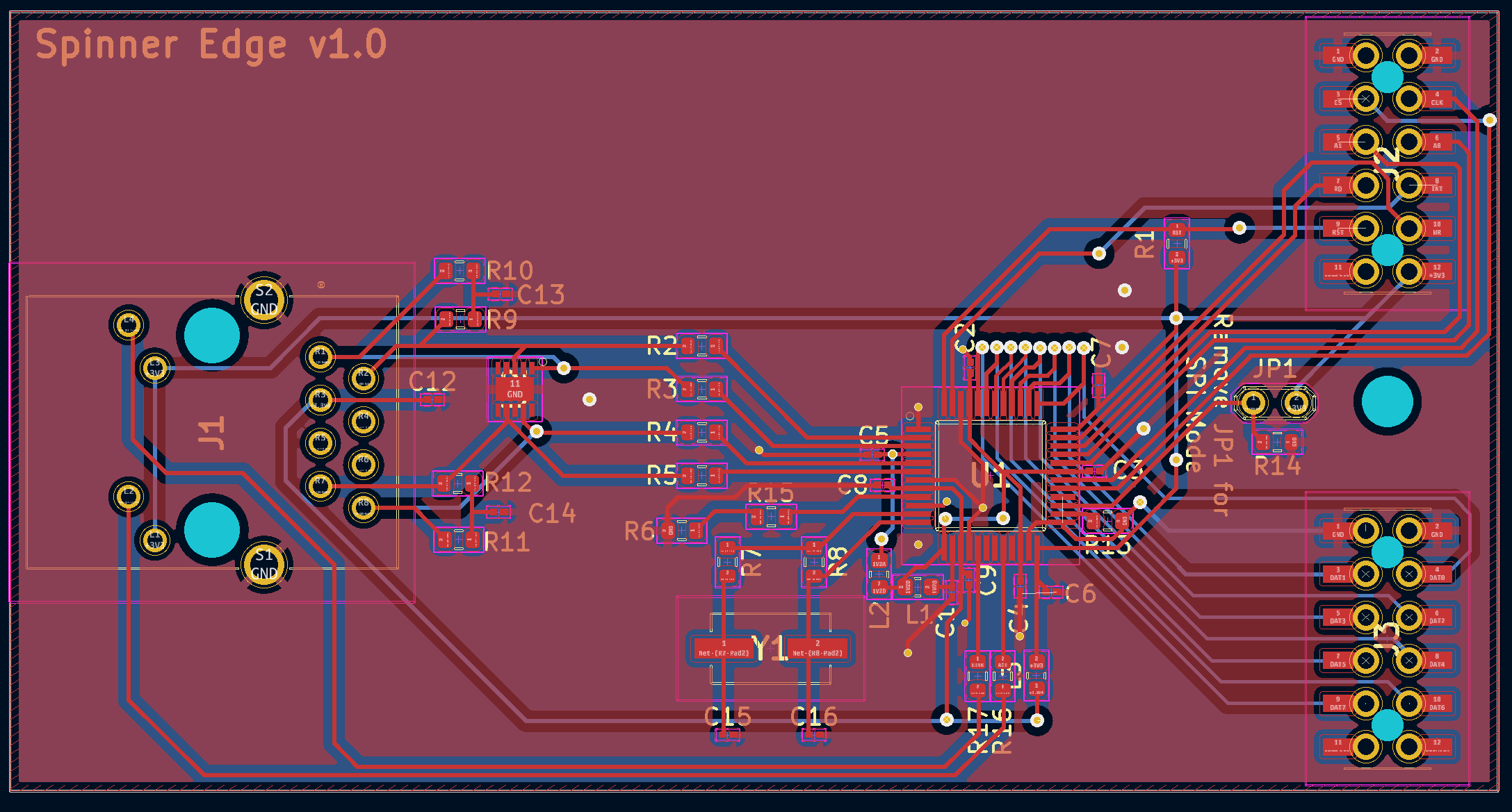
So I decided to make an attempt at a standalone Ethernet board based on the Wiznet W6100L. I had to jump through hoops so that the pins align with my light controller board. That's why tracks do not take the shortest path. This is also my first project in KiCad.
Please throw rocks at it, as I have limited experience with board layout. I don't feel good about all of the vias, but that seems to be the most practical way to cross traces.
Comments
You need a big notch between the pin headers to properly clear the ground posts. See Ray's RAM expander:
The official Parallax double boards have them, too, but I had the 96MB board image at hand to illustrate.
If you stick with the unplated hold to accommodate the ground posts, make sure it's big enough. The lugs on my Rev B and Rev C Eval boards are 0.145" (3.7mm) in diameter. The ground posts on the Edge breadboard are only 2.4mm.
@ke4pjw
LOL, I was thinking about doing a Wiznet board too in my next group of PCBs, but haven't yet got to it (though mine would be SPI only with the W5500 most likely).
Looking at all those P2 connector signals crossings, you might be better off swapping the pair of data and control pin signal groups around between the two 2x6 connectors as each group seems to line up with pins closer to the other connector vs the ones they are currently attached to. (EDIT: unless this was done to match your light controller board...?). Control signal order mapping is typically arbitrary from a software perspective (apart from address pins) so you should be able to route those quite cleanly. The data signal order could still require some layer swaps but it still might end up cleaner than what you have, so it's worth a look or a draft routing attempt to see if it helps. Also this side is a relatively low speed bus (14MB/s or so) and the layout there isn't really that critical vs the high speed Ethernet data side.
Is your PCB intended for 100Mbps operation or 10Mbps? For 100Mbps Ethernet the high speed side would need to be able to send it's symbols reliably at 125MHz. The data sheets on the particular devices you are using may include layout guidelines which could be worth reading through. That small 10 pin IC you have used seems to mess up the signals a bit and cause more crossings which may not be ideal. I think these are ideally length matched diff pairs so you want to route them carefully if you want best performance. Fast Ethernet isn't going to be as critical as GbE but it's still reasonably fast.
Some info for PHY board routing from TI which may be of use...though it may scare you a little. They do also mention to have no metal under the magnetics.
https://www.ti.com/lit/an/snla387/snla387.pdf?ts=1677402298573ref_url=https%3A%2F%2Fwww.google.com%2F
Also
https://www.pulseelectronics.com/wp-content/uploads/2020/12/Pulse_Layout-Considerations-v7.pdf
Just read up what you can on Ethernet layouts etc and try to make sense of it all...that's what I'd do anyway.
Also be careful along the board edges. You appear to have a via and traces on the right side fairly close to the cut edge. If you have spare room on the board you may want to shrink the total size to keep the trace lengths short where they are high speed and move the main QFP up a bit too to balance it a bit more on the board unless you have other constraints that affected this choice (you'd mentioned aligning pins with other boards....).
There was also this related Propeller 2 thread too...
https://forums.parallax.com/discussion/174246/wiznet-wiz6100-actually-wiz610ml-board-layouts
That's a lot of pins. How many cogs can you afford to spend on networking? I'm very slowly making progress on an IP stack for @ManAtWork 's 100Mbps Ethernet PHY addon board, which only uses 8 I/O. I'm fairly confident I'll be able to do it all in two cogs: one to deal with the hardware and one in Spin running all the higher-level stuff, hopefully including user data and timer callbacks.
@Wuerfel_21 and @JonnyMac I checked and the hole I have for the ground post is 3 MM. That's a little too close for comfort. I may have to revise the layout to support the Eval boards. Thanks for making me double check that!
@rogloh Thanks for the thorough look and links to documentation. The U2 device is a RCLAMP3304NATCT used for ESD protection. It is used on the wiz610mj that I modeled my schematic from. My magnetic is the only thing different. After looking for more info as you suggested, I found another board that Wiznet built. It uses the exact magnetic that I chose and does not have the ESD chip. I can't find any documentation saying that the ESD is built into the RB1-125BAG1A magnetic. I think I should keep it. Not sure. This Wiznet device is limited to 10 and 100 Mbps. The transmission lines are less than 2 inches, which I think is best practice. Also the magnetics are also more than an inch away from the PHY, which I think is also best practice. I may try to lay them out differently, to keep them the same distances from each other. Not sure I can do it any better though.
@Electrodude My driver is cogless. It uses locks for the various cogs to access the Wiznet. I do have a dedicated cog in my light controller for E1.31. It has it's own driver code to talk to the Wiznet, but it also uses the same lock mechanism, the main driver uses. The webserver, updater, ethernet status, etc all just make calls to the specific socket through the same driver code. (Though, they may all run in different cogs)
I will be happy to help test any of the code for @ManAtWork 's board. I have one, but every time I look at what it takes to build a TCP/IP stack, my eyes glaze over. The bookkeeping is what I can't get my mind around. All of that is hidden with the Wiznet. The down side of the Wiznet is that it as god awful UDP performance. You can't get data out of it faster than the buffer fill rate. I have to use 10Mbps to ensure I don't have dropped UDP packets.
@ke4pjw Looking good, watch for ground post clearance, as already mentioned.
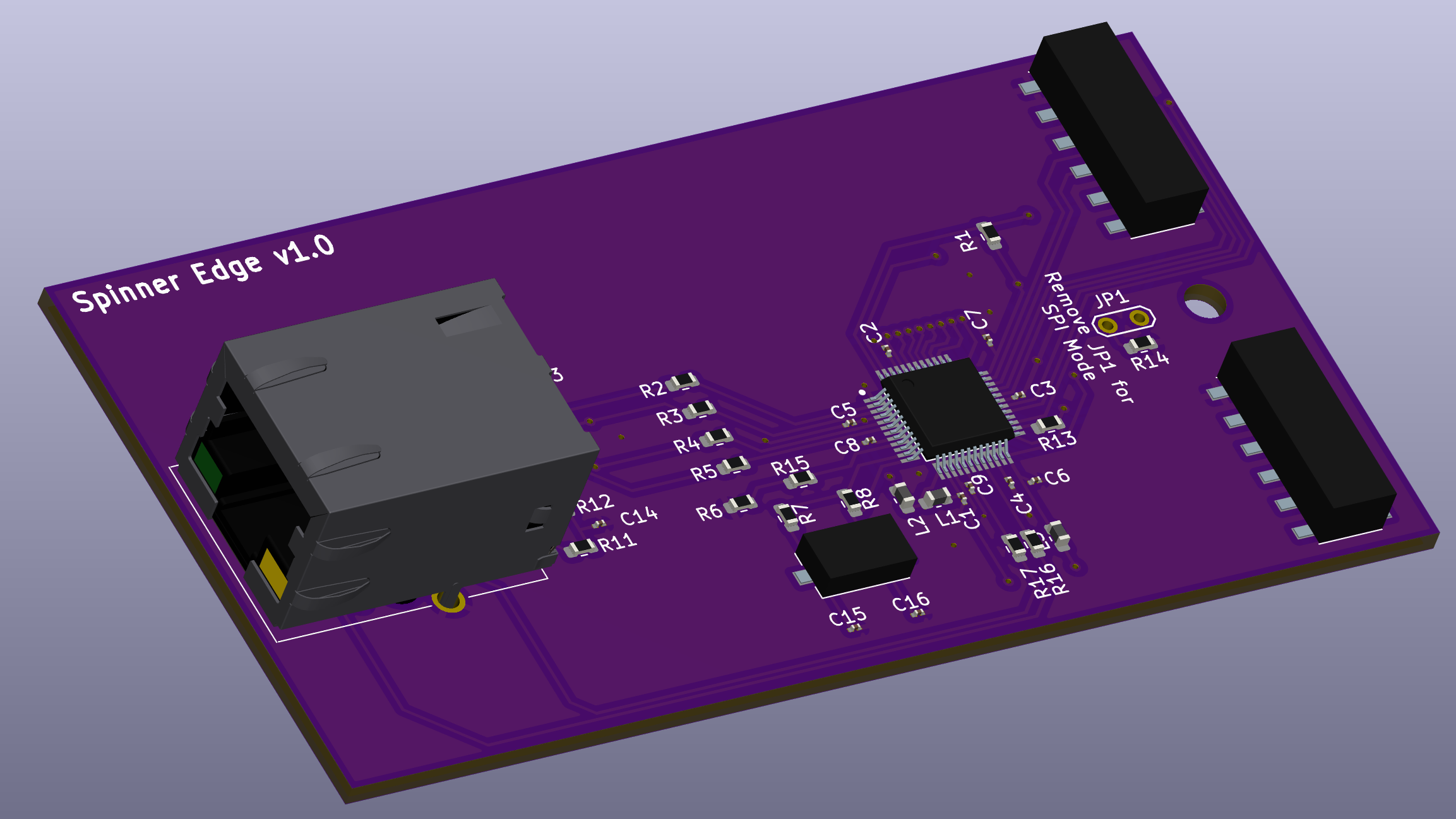
I've been doing like Parallax and have the connectors really close to the edge.
This prevents a lot of routing behind the connector, but I've been able to get by...
Probably doesn't matter much though... Maybe helps you see better when plugging it in?
I'm curious about the use of 8 data pins (think that is what you are doing) versus regular SPI.
I was able to get a Wiznet module working with SPI fairly easily.
Any idea of the throughput advantage with 8 data pins? Is it around 8X faster?
Also, in your applications, do you see using the bus constantly?
Or, do you think it could be shared with something else like memory or display?
Thanks @Rayman! I chose to do the parallel interface because it was easy. I did not use Wiznet's code for my driver. I it is written in spin2 and inline pasm. If I get time, I may go back around and implement the SPI interface in my code. As to it's performance, I know it is slower than 100mbps. At least with my sloppy layouts. It's specked at 4 clks for parallel read (25Mhz) and 70Mhz for SPI.
Yes, I hammer the bus continuously. I do not use the Int line. I think I will bring that out on a single jumper, in case people want to use it. My listeners continuously check to see if data is available. When data is available, it checks again to see if the buffer has changed. If it hasn't, it grabs the data in the buffer and updates the pointer.
The bus could be shared. Each device driver would have to obtain a lock. Once it has the lock, it could manipulate the address lines as needed and communicate via the bus. Each call to access the Wiznet in my driver is atomic, therefore, different processes (web,status,E1.31) may be in the middle of the process as a whole, but can't stall the bus. I hope that makes sense.
@ke4pjw Since you asked for feedback... I'm seeing a lot of empty space. Appears to be the board could be a lot smaller.
Probably doesn't matter electrically though...
Kudos to you for figuring out how to use the raw chip instead of just getting a module like I did.
A one header SPI version might be more interesting to me for things I have in mind...
There are some applications where I can't use wireless, and only need to relatively send small amounts of info...
SeeedStudio Fusion is pretty nice for low cost boards and stencils, although takes a while to deliver...
Also, I think the Ethernet connector usual goes past the edge of the board. Might be some problems as shown above…
My first smt boards were probably complete disasters. Hope you have better luck!
There's also the possibility of using one of the Wiznet SMD modules in a board design assuming you can source one easily - that could be the hardest part IMO. They make both W6100io and W5500io based modules, although these are SPI only. For my use I sort of liked the idea of making a simple carrier PCB basically with just a magjack and the 2x6 P2 header fitted on a single wide expansion PCB along with one of these modules. It should be relatively easy to assemble and could probably just about fit on a "standard" 20x40mm sized PCB. See here:
https://www.wiznet.io/product/network-module/
Of course it is easier still just to make some type of adapter PCB for the Wiz850io module with its inbuilt magjack but that wouldn't line up as nicely with all other connectors (if that matters to you). My plan was to undermount the W5500io module and have the RJ45 connector on the top, lined up with all other breakout connectors etc. It could be quite clean if it fits. Top PCB surface would visibly just have the SMD 2x6 connector and the RJ45, a bit like what I did for my audio breakout board here... https://forums.parallax.com/discussion/comment/1546310/#Comment_1546310
In addition to Ray's comments, I'm wondering if you're really going to use 0402s on a homebrew board. That's gutsy!
@Rayman I updated the board to give groundplane clearance the same as is on the WZ610MJ from Wiznet. I also shortened the board to allow the connector to hang off the edge of the board like the WZ610MJ. Yeah, I need to just bite the bullet and do some SMT layout and build those skills. I am sure this will be a disaster, LOL. Maybe it will work, we will find out! I am sure I could make better use of the space. The cost is the same either way.
@rogloh I agree that the W6100io is the way to go is you only want to support SPI. I wanted to use the parallel interface. I have about a dozen of the WZ610MJ boards out in the wild used in my light controllers. They do both SPI and parallel and are available directly from Wiznet. They sent me a nice shipping tray for them")
This project is just a way for me to prove out that I can make the SMD stuff work. Next step is to integrate it into the next iteration of my light controller. I am going to add a 3 port switch to it so that you can chain them together, if needed. Most likely going to use this fella right here. https://www.microchip.com/en-us/product/KSZ8863
Hopefully it will work. Fingers crossed!
I was looking at it last night. My god those are tiny! If I'm going to be stupid, I better be tough. I hope I am tough enough for those little fellas! LOL
PS those are 0603s
There are two sizes shown and the caps look very small ?
I've found 0805 are the fastest to manually place and solder, any smaller and the time increases, and quality decreases.
Unless you really need small size, it's better to use what is fastest to assemble.
A sparse board like above has a ton of room.
for resolving the J2, J3 cross connections to the P2, can you put them on the other side of the board together with J1 ?
SMD on one side, connectors on the other side.
And maybe put some screw holes on the edges so we can use the board and mechanical fix it in customized projects
5c
Sometimes if there’s extra space on a board, I’ll put in a little prototyping area, thru hole or smt or both …
0603 is OK but 0805 is a lot easier….
Also, 0603 doesn’t seem to save as much space as you’d think…
So I was going by the metric codes. The 0603 metric is much smaller than the 0603 imperial. I assume you all referring to the imperial size? Is imperial what is typically referenced?
Ok, I had to google it:
0805 or (2012M) = 2 x 1.25 mm (length x width) which is 0.08 x 0.05 inches.
0603s are manageable, but 0805s are much easier to deal with. I think the patterns you want to look at in KiCad are
This assumes you have a reflow setup. If hand soldering, they have patterns with bigger pads to help that process (which is not fun) .
I frequently find myself doing a search on things like "0603 resistor dimensions" to find tables like this for reference. You can see where the KiCad naming convention comes in.
Thanks guys! Ok, this evening I will change the caps and resistors to 0805 (2012M). The smaller parts are already on order, but I will update the BOM and order the larger components. At least those are the "cheap" parts.
Once I have "hands on" with the other parts, I can validate the through hole parts of the layout. The 3D rendering of the magnetic jack does not match the footprint or the datasheet.
You can put 0603 parts on 0805 pads if you need to...
At least, if hand soldering...
I would just keep it as 0603 though. It's not a huge difference.
This happens. Because of the work I do, I'm very fussy when it comes to visuals and can't always rely on parts others have made. Before I installed KiCad I already had a bit of experience with FreeCad and often make my own models, or modify those crafted by others. Check with the manufacturer for a model; those tend to be high-quality and much more reliable. For example, this is the model for the M20-7810645 that got from the vendor which is much more accurate that then simple cuboid that is in the library from Mouser.
Vendors data sheet trumps a 3rd party 3D model, and a real part in your hand, trumps the data sheet")
Those a LED pinouts?, so they will likely be formed the same each side, which makes the 3D 'in error'.
Kicad has specific 'handsolder' footprint versions for things like 0603 and 0805 passives. These have a bit longer, and perhaps a bit wider, pads that are a bit easier to hand solder
Just a comment on hand soldering tiny SMT parts: if you use an air pencil with good low-temp leaded paste, its a LOT easier. I do 0402 with not much effort just by holding the part down with a sharp dental pick and hitting it with the air pencil. The pick is key. And use a very hot airflow so you can get on it and get off fast. Use of a convective preheater under the board makes it easier too. Use GootWick and micro-tweezers for fixing any mishaps.😝
I dont have great vision, but I do have a cheap video microscope, and with the technique above, that makes the impossible possible for me.
@Tubular Thanks for the heads up about the handsolder footprints!
@JRoark that's exactly what I was planning. I have an air rework station that I was going to use. I was planning to get the stencil with the board and use solder paste. I have a little experience with it. Had to replace a couple of components in my Kenwood TM-D700, as well as many MicroUSB ports of the kids' Kindles. If this goes well, I am thinking of buying a cheapo reflow oven off ebay for ~$170.
OK, so I decided to just change the caps to 0603 (1608M) to match the resistors and inductors. I had additional schematic errors that needed to be corrected in both the schematic and the layout. I am not happy with all the vias. I think I just need to get over feeling about using the vias.
Based on the tolerances of the fab, I am not seeing any errors that would indicate they can't produce the board. I should be receiving the magnetics and other components this evening. If the dry fitting works on my printouts, I will order a handful of boards.
I added a spiderweb to the silkscreen as a homage to the P1 Spinneret.
Does U2 have another package option ?
0.5mm DFN/QFN parts can be a real pain to manage manually.
Extended footprint fingers can help a little, but they are still best avoided, if possible.