WIZnet WIZ6100 (actually WIZ610ML) board layouts
 Scroungre
Posts: 161
Hi All,
What I have here are no less than three different circuit board layouts, each intended as an ‘adapter’ from a Propellor 2 development board to a WIZnet WIZ610ML Ethernet module. None have been built nor tested yet.
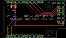
1 is for an SPI interface. Simple, but probably not very fast. Uses one 12-pin connector. It is distinctly ‘handed’ – the WIZnet module is not in the middle – in order that other slightly “too wide” devices can be used with it, given a few selected connectors. The board is 1.75” x 1.00”, and the WIZnet module is expected to very much overhang one edge.
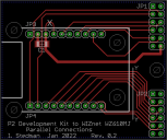
2 is for a Parallel interface, with a P2 Edge (JohnnyMac) breadboard, using two connectors. The board is 2.10” x 1.75”, and the WIZnet module is expected to very much overhang one edge. It could be smaller. It also has ‘hacking’ instructions for making it work with SPI.
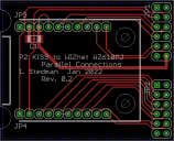
3 is also Parallel, but with connector spacing for a KISS000x board. Mostly because I wanted one. The board is 1.80” x 1.45”, and the WIZnet module is expected to very much overhang one edge. The ‘hacking’ instructions from #2 will still work, but they’re not documented.
About all of them:
All were done in CadSoft’s Eagle rev. 7.6 (the last one BEFORE AutoDesk bought it).
All are two-layer designs.
With one exception, all traces are on the ‘top’, and the bottom layer is a solid ground plane.
There is no silkscreen on the back.
The capacitor is an 0.1uF 3.3V (min.) monolithic in the 1206 SMT size. It’s optional.
Pin #1 on all connectors is denoted by a square pad.
The pin connections on the two parallel boards are the same.
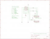
The pin connections on the SPI board are wackily different (to the P2).
Check the schematics.
I have not put together manufacturing files. I expect to tinker with them through a few more revisions before sending them off to be made. They have NOT been built nor tested (Yet. We might get around to it someday).
Files supplied shall be (sooner or later):
.png, pretty pictures that everyone can look at
.brd, the board layouts, in CadSoft’s Eagle format
.scm, the schematics, likewise.
I’ll post the .png’s first.
Use At Your Own Risk.
Comments, questions, suggestions, and even criticisms are invited. Insults will be replied to in kind or ignored at my discretion. Feel free to sniff around the layouts or schematics to see if I’ve blundered somewhere – could happen, I put these together on an otherwise idle Saturday afternoon. Apparently I don’t have enough to do (ha ha). Thanks anyhow, for putting up with me so far. S.




Comments
I would recommend you started from the plans which wiznet released for the said ethernet module and modified it into a nice 1 pcb solution.
https://github.com/Wiznet/Hardware-Files-of-WIZnet/tree/master/05_Network_Module/WIZ610MJ/WIZ610MJ_V100
You're right, that would make a better board - and if I wanted to make 10,000 or so of them, I would do that. I mean, ideally, if you wanted fast Ethernet and a Propellor 2, you'd put both chips on the same board, and off you go - but that's just wildly impractical from where I'm sitting here today.
But I don't want 10,000 of them. I don't have the tools or the skills to assemble very small and fine-pitch chips. In short, despite the documentation, I couldn't build one (at least, not easily, not without a lot more gear, and a lot more practice, and even then there'd be reliability issues).
But I can purchase module A, and plug it into a little PCB, and then into module B, and have a good chance of it working soon, and not have to muck around with wiring by hand.
These things I can build.
And they'll work a lot better than breadboarding. S.
If the control pin mapping is somewhat arbitrary, even though the P2 is pretty flexible with pins I would typically have A0 and A1 on an aligned nibble or byte boundary of the IO pins. Doing such things can often help the software down the track especially if the streamer is used. In this particular case it may not actually matter (I didn't check the WIZ610 bus protocol), but that's just me trying to assist both software and hardware sides. It's always good to check how optimized software would use the pins before locking them down.
I am in optimization mode for my W6100 driver. Imma steal this idea for A0 and A1 lines
Hm! On the parallel ones, definitely.
On the SPI one, I put all the SPI signals (SCK, MOSI, MISO, and /CS) on one nibble, but in no particular order. The various SPI drivers I found floating about looked like they could handle arbitrary pin numbers. If that is not the case... Uh-oh. S.
Okay. So I've really just 'moved them down one', so A0 and A1 are on a nibble boundary at bit positions 4 & 5. The interrupt remains on bit position 0 - I heard that was nice too. Turned out the layout updating was near trivial - took about ten minutes, for both the parallel boards.
Putting A0 and A1 at bit positions 0 & 1 might be a bit trickier, but still readily doable, I believe. Might take half an hour...
This is the sort of thing I'm looking for when I post early revisions of board layouts! Typically, I wind up doing both software and hardware and updating them each as I go, but I'm taking advantage (thanks!) of lots of other people being better at Prop2 programming than I am. S.