Yeah in a little more debugging I just found it failed on lack of pull up. Let me see if these resistors controlled by the DIP switch are actually are connected when I find the right schematic. I thought some of this detects a pullup inside the SD card itself, but that might be different code.
@rogloh said:
FIXED! My boot sector is running now.
In your commented out code I re-enabled for this it appears it had the CLK and CS pins reversed.
Ouch! And it is even written in the comment that it is the serial flash CS... don't know where I got it, I checked the Catalina source and are correct there.
Maybe the SD adapter will work after all... have to check...
Hey @macca, in your arbiter's repo transfer command long it might be good to use a bit to distinguish code access from data access so that prefetch can be engaged for code accesses and skipped for data. It also might be good to have a way to select either 8 or 16 bit read transfers too which could help accelerate things when you know you want to read a 16 bit quantity instead of doing two 8 bit reads.
Writes would be harder to do at 16bits if you need to pack the data and the address and command into the same long, but if you were to read the 16 bit write data quantity from some HUB area (only) when you indicate it's a 16 bit write it might not be too bad and would save doing a separate 8 bit write transfer to PSRAM (and involve the arbiter a second time). Even though it adds a little more latency to transfer via the HUB in this particular 16 bit case I think it'd be still faster than doing two individual writes.
@rogloh said:
Hey @macca, in your arbiter's repo transfer command long it might be good to use a bit to distinguish code access from data access so that prefetch can be engaged for code accesses and skipped for data. It also might be good to have a way to select either 8 or 16 bit read transfers too which could help accelerate things when you know you want to read a 16 bit quantity instead of doing two 8 bit reads.
Writes would be harder to do at 16bits if you need to pack the data and the address and command into the same long, but if you were to read the 16 bit write data quantity from some HUB area (only) when you indicate it's a 16 bit write it might not be too bad and would save doing a separate 8 bit write transfer to PSRAM (and involve the arbiter a second time). Even though it adds a little more latency to transfer via the HUB in this particular 16 bit case I think it'd be still faster than doing two individual writes.
I think I'll drop the prefetch queue concept, most emulators consider it always filled, the extra cycles are added to the jump instructions (the first instruction after a jump always takes 4 cycles for the opcode fetch, then it depends on the instruction itself... I don't think it is worth the effort). But doing 16 bit transfers for code seems a good idea, the opcode and modrm byte (if used) are available in one shot, will have to test this.
BTW, I ran some simple timings to see how things are going with PSRAM vs. HUB and to test some simple optimizations, here are the results (i_tstamp1 are the P2 clock cycles):
Timings are taken from the client before the request wxpin and after the result rdpin (or completion waitse for writes).
And another fun fact: after wxpin, it needs another 3 instructions (or 6 clocks) before pollse1 can actually clear the event (or the event is raised, depending on your point of view) ...
Looks interesting. PSRAM is about 2x the cost vs HUB (if using your arbiter path) and writes are about 50% more costly. For a 320MHz P2 this seems like it still probably falls within a regular bus transfer time anyway, at least for a 4.77MHz machine. I think the original PC's needed about 4 clocks per x86 bus cycle. So perhaps PSRAM P2 optimizations like pre-fetch are not going to be needed (at least right away). Good thing is there is scope there if needed.
One other approach is to use the FIFO for reading x86 instructions and just have the arbiter tell the x86 or DMA clients when to continue. The FIFO could be setup to wrap, and the arbiter COG could track where to read PSRAM data into, so the x86 core could do RFBYTE or RFWORD instructions to read the data instead of via the repo mode long itself.
Ouch! And it is even written in the comment that it is the serial flash CS... don't know where I got it, I checked the Catalina source and are correct there.
Maybe the SD adapter will work after all... have to check...
Does your "cheap arduino-target thing" has one of those permanently-enabled "74VHC125 quad buffers with 3-state outputs", and some 3.3kOhm resistors "implanted" into its lanes, like the ones shown at:
Because, if the above figure is a replica of your adapter, the "MISO"-output brought by the "125" will be in direct conflict with the SPI DO at P2_IO58 pin due to the absence of a 240Ohm series-resistor, which is present on newer boards that are already equipped with the SD card connector.
The intention of the series-resistor is to "mitigate" any conflicting "logic-level-battles", between SPI flash's DO, and Micro SD DAT0/MISO, which uses to plague that lane (P2_IO58) (a problem that was detected early-on the development cycle, and is documented elsewere, in many threads, at the forums).
Since I can't test it, I'm unsure which route will work better in your situation:
simply insert a 240Ohm in series, between the "125"-buffer output at MISO, and check if this solution will not "create" more conflicts with the SPI Flash DO-output than solve any of them; I'm also unsure about this solution, due to any extra timing delays , as the ones introduced by preserving the "125";
completelly remove the "125"-buffer and all those 3.3kOhm series-resistors (or simply "jump" three of them with some kynar wire), and substitute the one at MISO by a 240Ohm-one, or even use a 260Ohm resistor, in parallel with the remaining 3.3kOhm-one, which will also give ~240 Ohm.
@Yanomani said:
Does your "cheap arduino-target thing" has one of those permanently-enabled "74VHC125 quad buffers with 3-state outputs", and some 3.3kOhm resistors "implanted" into its lanes, like the ones shown at:
The adapter is like this:
Just some resistors and an regulator that can be bypassed with the 3.3v direct pin.
Since I can't test it, I'm unsure which route will work better in your situation:
simply insert a 240Ohm in series, between the "125"-buffer output at MISO, and check if this solution will not "create" more conflicts with the SPI Flash DO-output than solve any of them; I'm also unsure about this solution, due to any extra timing delays , as the ones introduced by preserving the "125";
completelly remove the "125"-buffer and all those 3.3kOhm series-resistors (or simply "jump" three of them with some kynar wire), and substitute the one at MISO by a 240Ohm-one, or even use a 260Ohm resistor, in parallel with the remaining 3.3kOhm-one, which will also give ~240 Ohm.
Thanks but for all that efforts I'll be happy with it on its own pins...
Just some resistors and an regulator that can be bypassed with the 3.3v direct pin.
Thanks but for all that efforts I'll be happy with it on its own pins...
You're welcome, but, if my eyes are not failling bad, the four resistors seems to be equal-valued (10kOhm), so they're just pull-ups. That board would be still missing the possibility of inserting a 240Ohm series-resistor...
@Yanomani said:
You're welcome, but, if my eyes are not failling bad, the four resistors seems to be equal-valued (10kOhm), so they're just pull-ups. That board would be still missing the possibility of inserting a 240Ohm series-resistor...
Yes, but adding a series resistor with a breadboard is easier than desoldering an smd chip...
Anyway, it works with the correct SD card pin assignments, however with the 240 ohm series resitsor works at 160MHz but fails at 320MHz, replaced with 120 ohm works also with 320MHz.
Not sure if this may cause problems to the flash chip.
Fantastic! Your board and this reply seems to almost answer two long-unsolved questions that are kind of recursive when it comes to that subject.
As it comes to my mind, they are:
are pullups on SD card control/data pins kind of a bennefical thing, or would they tend to represent just one more complication, than a good solution?
in terms of SD card access time, are there any real speed gains that can be achieved, by changing the 240Ohm series-resistor value (and, eventually, tottally rulling it out)?
The third question is kind of a consequence from the second, and you also named it: can the 240Ohm series-resistor, inserted between SD card DAT0/MISO and SPI Flash DO/P2_IO58 be removed, or substituted by a lower-valued one, without any long-term chance of damage to the SPI Flash itself?
@Yanomani said:
Fantastic! Your board and this reply seems to almost answer two long-unsolved questions that are kind of recursive when it comes to that subject.
As it comes to my mind, they are:
are pullups on SD card control/data pins kind of a bennefical thing, or would they tend to represent just one more complication, than a good solution?
in terms of SD card access time, are there any real speed gains that can be achieved, by changing the 240Ohm series-resistor value (and, eventually, tottally rulling it out)?
The third question is kind of a consequence from the second, and you also named it: can the 240Ohm series-resistor, inserted between SD card DAT0/MISO and SPI Flash DO/P2_IO58 be removed, or substituted by a lower-valued one, without any long-term chance of damage to the SPI Flash itself?
Thanks for your patience and commitment, @macca !
You are welcome!
Further testings revealed that while the flash seems to work and can be programmed, it won't boot anymore with the SD adapter plugged (with or without the card inserted), nor the boot from the SD works. I guess the permanent pullup on P59 prevents the boot... if I understand the dip switch table correctly, it means serial-only. I should try to remove the pull-up resistor from the adapter... not really a problem, never really used it expect for few tests and when I hit upload to flash by mistake... maybe another day...
Further testings revealed that while the flash seems to work and can be programmed, it won't boot anymore with the SD adapter plugged (with or without the card inserted), nor the boot from the SD works. I guess the permanent pullup on P59 prevents the boot... if I understand the dip switch table correctly, it means serial-only. I should try to remove the pull-up resistor from the adapter... not really a problem, never really used it expect for few tests and when I hit upload to flash by mistake... maybe another day...
Perhaps not exactly due to the presence of the pullup by itself, but due its "low" value (10kOhm); maybe trading it for a 50kOhm-one (in fact, trading all of them) can reveal as the "innermost-guts" of the trick.
P.S. my mistake, since I forgot almost everything about the influence of the pullups on the boot-decision tree...
@TonyB_ said:
1111111x xx111xxx is an alias of PUSH r/m.
The 8086 has no real NOPs and every opcode does something.
Are you sure? I distinctly remember 90h being a NOP.
Z80 00H really does nothing and is a true NOP.
8086 90H exchanges AX with AX and is NOP in effect.
That was my point.
Ah
And that's the nice thing about emulators. You can just ignore instructions that function as NOPs. Similar with FWAIT. If you only emulate FP routines to run in the same core, then you don't need it. But if you put it in another thread or in other hardware, then you'd need it for syncing.


Comments
Yeah in a little more debugging I just found it failed on lack of pull up. Let me see if these resistors controlled by the DIP switch are actually are connected when I find the right schematic. I thought some of this detects a pullup inside the SD card itself, but that might be different code.
FIXED! My boot sector is running now.
In your commented out code I re-enabled for this it appears it had the CLK and CS pins reversed.
Ouch! And it is even written in the comment that it is the serial flash CS... don't know where I got it, I checked the Catalina source and are correct there.
Maybe the SD adapter will work after all... have to check...
Hey @macca, in your arbiter's repo transfer command long it might be good to use a bit to distinguish code access from data access so that prefetch can be engaged for code accesses and skipped for data. It also might be good to have a way to select either 8 or 16 bit read transfers too which could help accelerate things when you know you want to read a 16 bit quantity instead of doing two 8 bit reads.
Writes would be harder to do at 16bits if you need to pack the data and the address and command into the same long, but if you were to read the 16 bit write data quantity from some HUB area (only) when you indicate it's a 16 bit write it might not be too bad and would save doing a separate 8 bit write transfer to PSRAM (and involve the arbiter a second time). Even though it adds a little more latency to transfer via the HUB in this particular 16 bit case I think it'd be still faster than doing two individual writes.
I think I'll drop the prefetch queue concept, most emulators consider it always filled, the extra cycles are added to the jump instructions (the first instruction after a jump always takes 4 cycles for the opcode fetch, then it depends on the instruction itself... I don't think it is worth the effort). But doing 16 bit transfers for code seems a good idea, the opcode and modrm byte (if used) are available in one shot, will have to test this.
BTW, I ran some simple timings to see how things are going with PSRAM vs. HUB and to test some simple optimizations, here are the results (i_tstamp1 are the P2 clock cycles):
HUB:
PSRAM:
Timings are taken from the client before the request wxpin and after the result rdpin (or completion waitse for writes).
And another fun fact: after wxpin, it needs another 3 instructions (or 6 clocks) before pollse1 can actually clear the event (or the event is raised, depending on your point of view) ...
Looks interesting. PSRAM is about 2x the cost vs HUB (if using your arbiter path) and writes are about 50% more costly. For a 320MHz P2 this seems like it still probably falls within a regular bus transfer time anyway, at least for a 4.77MHz machine. I think the original PC's needed about 4 clocks per x86 bus cycle. So perhaps PSRAM P2 optimizations like pre-fetch are not going to be needed (at least right away). Good thing is there is scope there if needed.
One other approach is to use the FIFO for reading x86 instructions and just have the arbiter tell the x86 or DMA clients when to continue. The FIFO could be setup to wrap, and the arbiter COG could track where to read PSRAM data into, so the x86 core could do RFBYTE or RFWORD instructions to read the data instead of via the repo mode long itself.
Does your "cheap arduino-target thing" has one of those permanently-enabled "74VHC125 quad buffers with 3-state outputs", and some 3.3kOhm resistors "implanted" into its lanes, like the ones shown at:
https://m.media-amazon.com/images/I/61De17IVywL.AC_SL1500.jpg
Because, if the above figure is a replica of your adapter, the "MISO"-output brought by the "125" will be in direct conflict with the SPI DO at P2_IO58 pin due to the absence of a 240Ohm series-resistor, which is present on newer boards that are already equipped with the SD card connector.
The intention of the series-resistor is to "mitigate" any conflicting "logic-level-battles", between SPI flash's DO, and Micro SD DAT0/MISO, which uses to plague that lane (P2_IO58) (a problem that was detected early-on the development cycle, and is documented elsewere, in many threads, at the forums).
Since I can't test it, I'm unsure which route will work better in your situation:
simply insert a 240Ohm in series, between the "125"-buffer output at MISO, and check if this solution will not "create" more conflicts with the SPI Flash DO-output than solve any of them; I'm also unsure about this solution, due to any extra timing delays , as the ones introduced by preserving the "125";
completelly remove the "125"-buffer and all those 3.3kOhm series-resistors (or simply "jump" three of them with some kynar wire), and substitute the one at MISO by a 240Ohm-one, or even use a 260Ohm resistor, in parallel with the remaining 3.3kOhm-one, which will also give ~240 Ohm.
Hope it helps...
Henrique
The adapter is like this:
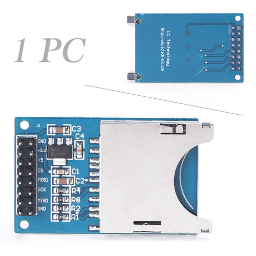
Just some resistors and an regulator that can be bypassed with the 3.3v direct pin.
Thanks but for all that efforts I'll be happy with it on its own pins...
You're welcome, but, if my eyes are not failling bad, the four resistors seems to be equal-valued (10kOhm), so they're just pull-ups. That board would be still missing the possibility of inserting a 240Ohm series-resistor...
Yes, but adding a series resistor with a breadboard is easier than desoldering an smd chip...
Anyway, it works with the correct SD card pin assignments, however with the 240 ohm series resitsor works at 160MHz but fails at 320MHz, replaced with 120 ohm works also with 320MHz.
Not sure if this may cause problems to the flash chip.
Fantastic! Your board and this reply seems to almost answer two long-unsolved questions that are kind of recursive when it comes to that subject.
As it comes to my mind, they are:
The third question is kind of a consequence from the second, and you also named it: can the 240Ohm series-resistor, inserted between SD card DAT0/MISO and SPI Flash DO/P2_IO58 be removed, or substituted by a lower-valued one, without any long-term chance of damage to the SPI Flash itself?
Thanks for your patience and commitment, @macca !
You are welcome!")
Further testings revealed that while the flash seems to work and can be programmed, it won't boot anymore with the SD adapter plugged (with or without the card inserted), nor the boot from the SD works. I guess the permanent pullup on P59 prevents the boot... if I understand the dip switch table correctly, it means serial-only. I should try to remove the pull-up resistor from the adapter... not really a problem, never really used it expect for few tests and when I hit upload to flash by mistake... maybe another day...
Perhaps not exactly due to the presence of the pullup by itself, but due its "low" value (10kOhm); maybe trading it for a 50kOhm-one (in fact, trading all of them) can reveal as the "innermost-guts" of the trick.
P.S. my mistake, since I forgot almost everything about the influence of the pullups on the boot-decision tree...
Are you sure? I distinctly remember 90h being a NOP.
Z80 00H really does nothing and is a true NOP.
8086 90H exchanges AX with AX and is NOP in effect.
That was my point.
Ah
And that's the nice thing about emulators. You can just ignore instructions that function as NOPs. Similar with FWAIT. If you only emulate FP routines to run in the same core, then you don't need it. But if you put it in another thread or in other hardware, then you'd need it for syncing.