

What should be ADC result when the pin is connected to the ground?
 pik33
Posts: 2,419
pik33
Posts: 2,419
in Propeller 2
I expected 0 or something near that
Now as I am testing 18-bit sinc3 mode I got something about $B300 (ground) and $34000 (3v3)
I got similar results while using another modes (scaled to their bit resolution).
The CPU clock is about 280 MHz
Zero / max appears if I set ADC gain higher than 1
I tested this with 2 different edge modules with the same results.
Is it normal?
Comments
You won't get zero until you calibrate for ground, then remeasure and remove the calibration value. I think it's correct to say that the ADCs measure from below ground to above Vdd.
Yes the ADC's have been deliberately designed to have around 5v span, so they can measure a little above and below the rails. (theoretically around -.085 to +4.15v is where the axes intercept). So 0v gives data approx 1/6 of full scale, and 3v3 about 5/6 of full scale, when using 1x mode.
To add to Jon's and Tubular's comments, there's no exact value for GND and VIO. Each pin is slightly different depending on tiny differences in the the ADC's resistors and inverter thresholds. And noise induced fluctuations also means a slight lack of stability to boot. There hasn't been a lot of detail on sucessfully using the ADCs for instrumentation. Chip almost seems to discourages it.
Best results I've heard of have been from cycling through measuring of GIO then VIO then Pin, and repeat. This method naturally incurs a large speed penalty as it destroys the pipelining effect having to reset the hardware filter after each source select change.
How does Chip discourage using ADCs for instrumentation?
Very early on (pre-sinc pipelines) we were using GIO-Pin-VIO-Pin so you're looking at the pin more (50%) of the time. You can improve further by making use of the strong correlation between GIO and VIO (as you know, you plotted this). So you don't necessarily need to look at GIO and VIO for as long as you're looking at the pin.
If you want you can use a second ADC pin to stare at the same signal while the other pin is calibrating. Or you can use the second pin to output GIO via 19 ohms to give you a local ground. Lots of flexibility
Richard (rjsm) published ~10 pages of ADC findings a few years back, can't find it at the moment
Perhaps you're talking about one of the the following thread contents:
https://forums.parallax.com/discussion/169602/characterizing-p2-eval-analog-performance
https://forums.parallax.com/discussion/170951/evaluating-p2-performance-capabilities
That second one had the PDF link, thanks Henrique. It's 18 pages of ADC goodness, rather than the 10 that I remembered
Maybe shies away for talking about it, would be more apt. The Effective Number Of Bits figure is disheartening. I've just run up Chip's millivolt to VGA demo and I'm seeing only about, 9 bits err make that, 10 bits effective with the ADC inputs tied to GND on an Eval Board. (Ie: 5 mV fluctuation in a 5 Volt span)
All those variations still require waiting on the filter to stabilise, on a per sample per source basis. The pipelining effect is utterly destroyed.
Hmm!
You're welcome, Lachlan!
Richard's work is a dependable reference, as always.
Just on the gain aspect, the gain is centred around the midpoint, about1.65v. So if using 10x gain, that 5v span becomes 1.65+/-0.25v, or ~1.4 to 1.9v
Okay, I've noticed that Chip kept the sampling resolution low in that demo. A quick tweak of setting the sample period from 512 ticks to 8192 ticks (and adding a decimal place) improves the noise floor to 1.5 mV from the earlier rough 5 mV. So a good 11.5 bits effective, maybe 12. Better but still needs more work.
11..12 bits in my experiments. Having a usable video driver I can start make stuff like "oscilloscope" to see what happens with these ADCs streams. I have several ideas how to extend the resolution using variable gain and/or more pins and/or process the raw bitstream but I have to see it first.
Did anyone try linking the ADC to an adjacent pin thats outputting a low, rather than GIO? This should significantly improve things as you're not sharing gnd with the 1v8 core
There is a concern with resistor accuracy. They're all tucked in under the VIO supply rail near the outer perimeter of the pad-ring. The analogue switches are 3v3 powered, so noise from 1v8 VDD is not one of the concerns.
I'd even hazard a guess there is cross talk on those resistors just like there was for PinB source. So clamping the pin might clean that up as well as eliminating the resistor mismatch issue.
Here's the left end of the schematic that Chip put up. At the top is the source select decoder. You can see even that is operating from VIO/GIO rather than VDD/GND.
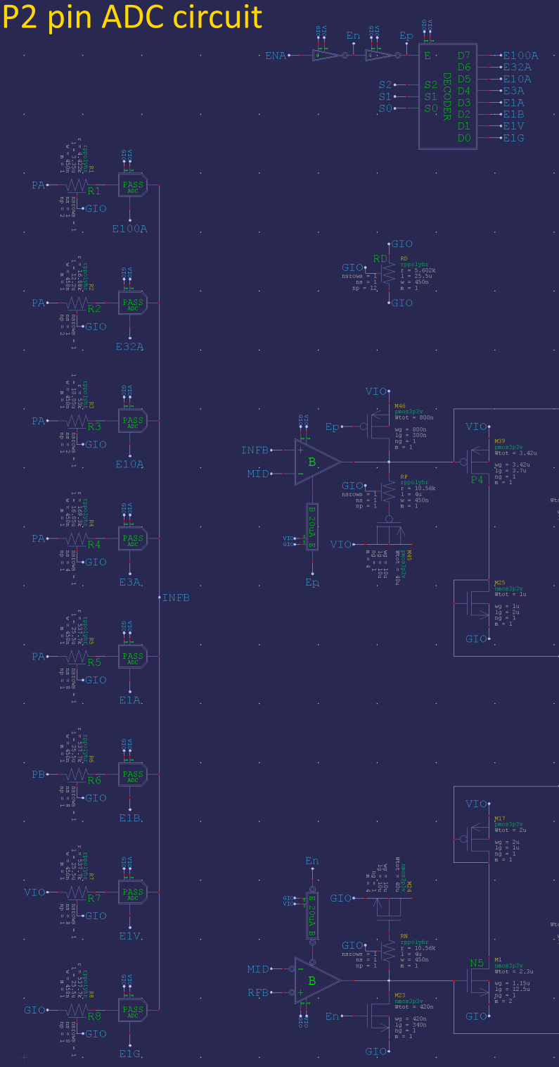
Evan consider the path from GIO in that schematic, to where you have the ground wire attached to the ADC input. What series elements does that ground traverse along the way? It shares a portion of its path with the 1v8 return current from the digital core, due to the single common ground connection. That heavier 1v8 return current runs along the same path for a way and since the resistance is small but finite, a small but finite 'ground rise' voltage is introduced, dependent on the core current being consumed.
I think this is why when you look at the standard deviation of VIO calibration readings, they are noticeably lower than the standard deviation of GIO calibration readings, on a like for like sampling basis. You should be able to see this if you connect the ADC jumper wire to 3v3 instead of ground, do the 'fluctuations' drop below 1.5mV?
The resistor mismatch isn't really an issue here, because the source resistance (of the jumper lead connecting ground to ADC) is many orders of magnitude less than the ADC input resistance.
You could check crosstalk by dropping the frequency right down, but this also drops the 1v8 core current, so it might be hard to separate and verify.
When you say "ADC input", are you meaning the I/O pin itself or the GIO supply for the ADC?
There is only one place that GIO is common with GND, and that's the hulking exposed thermal pad. Everything on die is local GIO only.
EDIT: Oh, you're asking about my jumper on the Eval board! Well, the GND plane is pretty all encompassing in the board. The header is directly into that for its GND pins. The exposed pad has a lot of vias to the GND plane. The I/O track is sandwiched between two GND layers I think.
I've run up Chip's millivolt demo again and tried the jumper on the VIO pin at the header, instead of GND pin. Found I had to reduce the sample period to 2048 ticks, because of an overflow somewhere in the code, rather than the larger 8192 I had used before. Interestingly this had no impact on the ENOB. Looking closer this makes it 2.2 mV instead of 1.5 mV.
With both the VIO position and GND position it's still about 1.5 mV 2.2 mV fluctuations. And changing back to sample period of 512 ticks also reproduced the 5 mV fluctuations with both jumper positions.
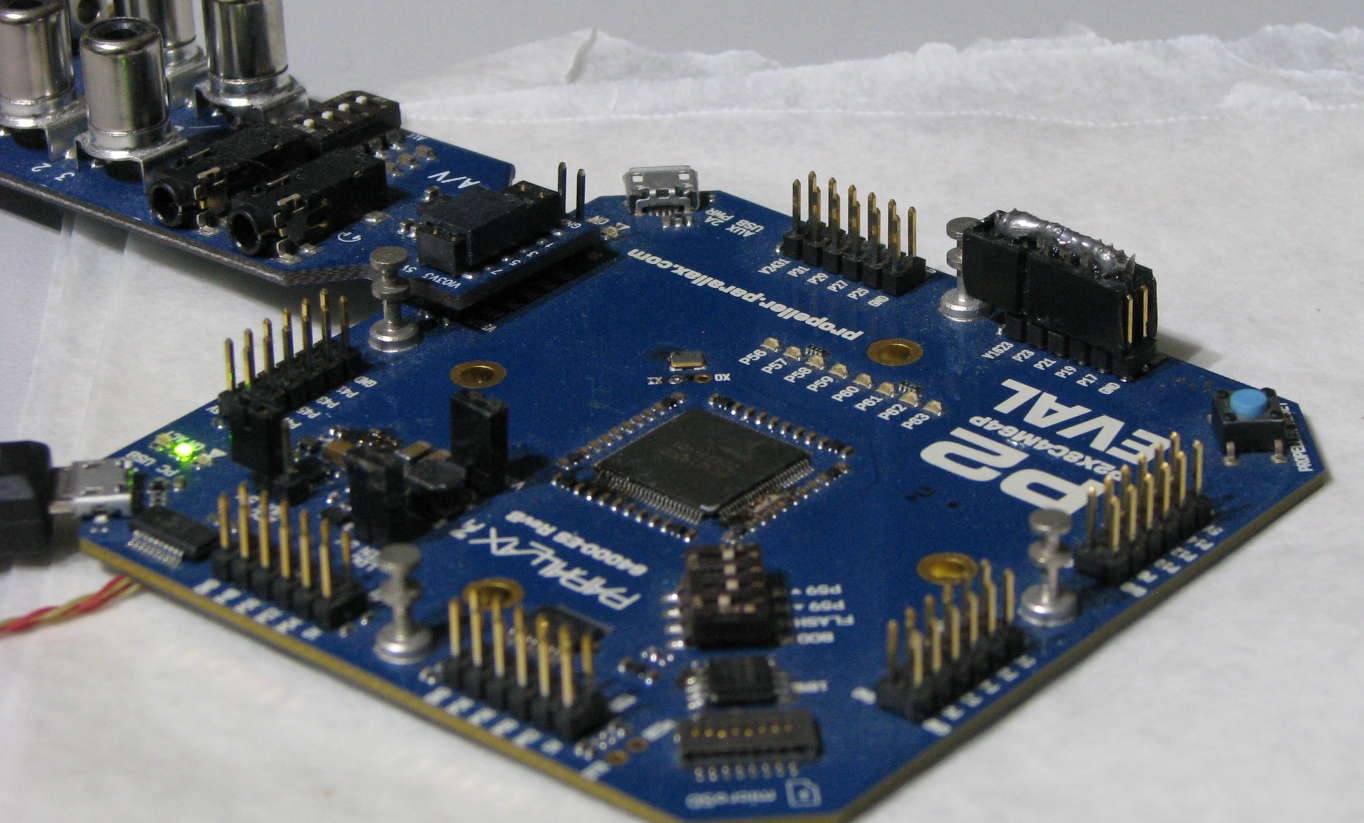
PS: Here's a photo of the jumper on P16..P23 to VIO:
I had a quick look at my theory about the common ground. Running normal 'video' programs at a few hundred MHz seems to raise the ground only by 0.07~0.1mV, and the shared path resistance seems to be of the order of 0.5 milliohms. Unless there are large switching current spikes I think there has to be something else causing the fluctuations you're seeing
I'll go and find those VIO / GIO standard deviation test logs tomorrow
I've been looking at Chip's code and discovered he's operating on a 2+8 sampling basis to get at least some pipelining going.
So the sequence is:
2 x GIO skipped, then 8 x GIO accumulated
2 x Pin skipped, then 8 x Pin accumulated
2 x VIO skipped, then 8 x VIO accumulated
2 x Pin skipped, then 8 x Pin accumulated